EP0805438B1 - Servo circuit - Google Patents
Servo circuit Download PDFInfo
- Publication number
- EP0805438B1 EP0805438B1 EP97302912A EP97302912A EP0805438B1 EP 0805438 B1 EP0805438 B1 EP 0805438B1 EP 97302912 A EP97302912 A EP 97302912A EP 97302912 A EP97302912 A EP 97302912A EP 0805438 B1 EP0805438 B1 EP 0805438B1
- Authority
- EP
- European Patent Office
- Prior art keywords
- signal
- circuit
- phase
- value
- supplied
- Prior art date
- Legal status (The legal status is an assumption and is not a legal conclusion. Google has not performed a legal analysis and makes no representation as to the accuracy of the status listed.)
- Expired - Lifetime
Links
- 230000003287 optical effect Effects 0.000 description 35
- 230000000630 rising effect Effects 0.000 description 31
- 238000010586 diagram Methods 0.000 description 20
- 238000012935 Averaging Methods 0.000 description 15
- 238000005070 sampling Methods 0.000 description 14
- 238000003708 edge detection Methods 0.000 description 13
- 238000001514 detection method Methods 0.000 description 8
- 239000004065 semiconductor Substances 0.000 description 8
- 238000012937 correction Methods 0.000 description 2
- 238000005259 measurement Methods 0.000 description 2
- 238000000034 method Methods 0.000 description 2
- 238000012545 processing Methods 0.000 description 2
- 238000006243 chemical reaction Methods 0.000 description 1
- 230000010354 integration Effects 0.000 description 1
- 238000012986 modification Methods 0.000 description 1
- 230000004048 modification Effects 0.000 description 1
- 230000006641 stabilisation Effects 0.000 description 1
- 238000011105 stabilization Methods 0.000 description 1
- 230000000087 stabilizing effect Effects 0.000 description 1
- 238000012546 transfer Methods 0.000 description 1
Images


Classifications
-
- H—ELECTRICITY
- H03—ELECTRONIC CIRCUITRY
- H03L—AUTOMATIC CONTROL, STARTING, SYNCHRONISATION, OR STABILISATION OF GENERATORS OF ELECTRONIC OSCILLATIONS OR PULSES
- H03L7/00—Automatic control of frequency or phase; Synchronisation
- H03L7/06—Automatic control of frequency or phase; Synchronisation using a reference signal applied to a frequency- or phase-locked loop
- H03L7/16—Indirect frequency synthesis, i.e. generating a desired one of a number of predetermined frequencies using a frequency- or phase-locked loop
- H03L7/18—Indirect frequency synthesis, i.e. generating a desired one of a number of predetermined frequencies using a frequency- or phase-locked loop using a frequency divider or counter in the loop
- H03L7/181—Indirect frequency synthesis, i.e. generating a desired one of a number of predetermined frequencies using a frequency- or phase-locked loop using a frequency divider or counter in the loop a numerical count result being used for locking the loop, the counter counting during fixed time intervals
-
- G—PHYSICS
- G11—INFORMATION STORAGE
- G11B—INFORMATION STORAGE BASED ON RELATIVE MOVEMENT BETWEEN RECORD CARRIER AND TRANSDUCER
- G11B19/00—Driving, starting, stopping record carriers not specifically of filamentary or web form, or of supports therefor; Control thereof; Control of operating function ; Driving both disc and head
- G11B19/20—Driving; Starting; Stopping; Control thereof
- G11B19/24—Arrangements for providing constant relative speed between record carrier and head
- G11B19/247—Arrangements for providing constant relative speed between record carrier and head using electrical means
-
- G—PHYSICS
- G11—INFORMATION STORAGE
- G11B—INFORMATION STORAGE BASED ON RELATIVE MOVEMENT BETWEEN RECORD CARRIER AND TRANSDUCER
- G11B19/00—Driving, starting, stopping record carriers not specifically of filamentary or web form, or of supports therefor; Control thereof; Control of operating function ; Driving both disc and head
- G11B19/20—Driving; Starting; Stopping; Control thereof
- G11B19/26—Speed-changing arrangements; Reversing arrangements; Drive-transfer means therefor
-
- G—PHYSICS
- G11—INFORMATION STORAGE
- G11B—INFORMATION STORAGE BASED ON RELATIVE MOVEMENT BETWEEN RECORD CARRIER AND TRANSDUCER
- G11B19/00—Driving, starting, stopping record carriers not specifically of filamentary or web form, or of supports therefor; Control thereof; Control of operating function ; Driving both disc and head
- G11B19/20—Driving; Starting; Stopping; Control thereof
- G11B19/28—Speed controlling, regulating, or indicating
-
- G—PHYSICS
- G11—INFORMATION STORAGE
- G11B—INFORMATION STORAGE BASED ON RELATIVE MOVEMENT BETWEEN RECORD CARRIER AND TRANSDUCER
- G11B20/00—Signal processing not specific to the method of recording or reproducing; Circuits therefor
- G11B20/10—Digital recording or reproducing
-
- G—PHYSICS
- G11—INFORMATION STORAGE
- G11B—INFORMATION STORAGE BASED ON RELATIVE MOVEMENT BETWEEN RECORD CARRIER AND TRANSDUCER
- G11B20/00—Signal processing not specific to the method of recording or reproducing; Circuits therefor
- G11B20/10—Digital recording or reproducing
- G11B20/10009—Improvement or modification of read or write signals
- G11B20/10222—Improvement or modification of read or write signals clock-related aspects, e.g. phase or frequency adjustment or bit synchronisation
- G11B20/1024—Improvement or modification of read or write signals clock-related aspects, e.g. phase or frequency adjustment or bit synchronisation wherein a phase-locked loop [PLL] is used
- G11B20/1025—Improvement or modification of read or write signals clock-related aspects, e.g. phase or frequency adjustment or bit synchronisation wherein a phase-locked loop [PLL] is used the PLL being discrete time or digital PLL
-
- G—PHYSICS
- G11—INFORMATION STORAGE
- G11B—INFORMATION STORAGE BASED ON RELATIVE MOVEMENT BETWEEN RECORD CARRIER AND TRANSDUCER
- G11B20/00—Signal processing not specific to the method of recording or reproducing; Circuits therefor
- G11B20/10—Digital recording or reproducing
- G11B20/14—Digital recording or reproducing using self-clocking codes
- G11B20/1403—Digital recording or reproducing using self-clocking codes characterised by the use of two levels
-
- G—PHYSICS
- G11—INFORMATION STORAGE
- G11B—INFORMATION STORAGE BASED ON RELATIVE MOVEMENT BETWEEN RECORD CARRIER AND TRANSDUCER
- G11B27/00—Editing; Indexing; Addressing; Timing or synchronising; Monitoring; Measuring tape travel
- G11B27/10—Indexing; Addressing; Timing or synchronising; Measuring tape travel
- G11B27/19—Indexing; Addressing; Timing or synchronising; Measuring tape travel by using information detectable on the record carrier
- G11B27/24—Indexing; Addressing; Timing or synchronising; Measuring tape travel by using information detectable on the record carrier by sensing features on the record carrier other than the transducing track ; sensing signals or marks recorded by another method than the main recording
-
- H—ELECTRICITY
- H03—ELECTRONIC CIRCUITRY
- H03L—AUTOMATIC CONTROL, STARTING, SYNCHRONISATION, OR STABILISATION OF GENERATORS OF ELECTRONIC OSCILLATIONS OR PULSES
- H03L7/00—Automatic control of frequency or phase; Synchronisation
- H03L7/06—Automatic control of frequency or phase; Synchronisation using a reference signal applied to a frequency- or phase-locked loop
- H03L7/08—Details of the phase-locked loop
- H03L7/085—Details of the phase-locked loop concerning mainly the frequency- or phase-detection arrangement including the filtering or amplification of its output signal
-
- E—FIXED CONSTRUCTIONS
- E05—LOCKS; KEYS; WINDOW OR DOOR FITTINGS; SAFES
- E05Y—INDEXING SCHEME RELATING TO HINGES OR OTHER SUSPENSION DEVICES FOR DOORS, WINDOWS OR WINGS AND DEVICES FOR MOVING WINGS INTO OPEN OR CLOSED POSITION, CHECKS FOR WINGS AND WING FITTINGS NOT OTHERWISE PROVIDED FOR, CONCERNED WITH THE FUNCTIONING OF THE WING
- E05Y2400/00—Electronic control; Power supply; Power or signal transmission; User interfaces
- E05Y2400/10—Electronic control
- E05Y2400/30—Electronic control of motors
-
- G—PHYSICS
- G11—INFORMATION STORAGE
- G11B—INFORMATION STORAGE BASED ON RELATIVE MOVEMENT BETWEEN RECORD CARRIER AND TRANSDUCER
- G11B2220/00—Record carriers by type
- G11B2220/20—Disc-shaped record carriers
- G11B2220/21—Disc-shaped record carriers characterised in that the disc is of read-only, rewritable, or recordable type
- G11B2220/215—Recordable discs
- G11B2220/218—Write-once discs
-
- G—PHYSICS
- G11—INFORMATION STORAGE
- G11B—INFORMATION STORAGE BASED ON RELATIVE MOVEMENT BETWEEN RECORD CARRIER AND TRANSDUCER
- G11B2220/00—Record carriers by type
- G11B2220/20—Disc-shaped record carriers
- G11B2220/25—Disc-shaped record carriers characterised in that the disc is based on a specific recording technology
- G11B2220/2537—Optical discs
- G11B2220/2545—CDs
-
- G—PHYSICS
- G11—INFORMATION STORAGE
- G11B—INFORMATION STORAGE BASED ON RELATIVE MOVEMENT BETWEEN RECORD CARRIER AND TRANSDUCER
- G11B27/00—Editing; Indexing; Addressing; Timing or synchronising; Monitoring; Measuring tape travel
- G11B27/10—Indexing; Addressing; Timing or synchronising; Measuring tape travel
- G11B27/19—Indexing; Addressing; Timing or synchronising; Measuring tape travel by using information detectable on the record carrier
- G11B27/28—Indexing; Addressing; Timing or synchronising; Measuring tape travel by using information detectable on the record carrier by using information signals recorded by the same method as the main recording
- G11B27/30—Indexing; Addressing; Timing or synchronising; Measuring tape travel by using information detectable on the record carrier by using information signals recorded by the same method as the main recording on the same track as the main recording
- G11B27/3027—Indexing; Addressing; Timing or synchronising; Measuring tape travel by using information detectable on the record carrier by using information signals recorded by the same method as the main recording on the same track as the main recording used signal is digitally coded
-
- H—ELECTRICITY
- H03—ELECTRONIC CIRCUITRY
- H03L—AUTOMATIC CONTROL, STARTING, SYNCHRONISATION, OR STABILISATION OF GENERATORS OF ELECTRONIC OSCILLATIONS OR PULSES
- H03L2207/00—Indexing scheme relating to automatic control of frequency or phase and to synchronisation
- H03L2207/50—All digital phase-locked loop
Definitions
- the present invention relates to a servo circuit, in particular, to a servo circuit having a speed control system and two phase control systems.
- the present invention also relates to a digital PLL circuit, in particular, to a digital PLL circuit which generates a clock signal which is in synchronization with pulses of predetermined pulse widths included in an input signal.
- the present invention also relates to an optical disk device, in particular, to an optical disk device which performs recording data on a recordable optical disk and reproducing data therefrom.
- US-A-5 170 386 on which the preamble to claim 1 is based, discloses a servo circuit in which the frequency and phase of a reference clock signal is composed to the frequency and phase of a clock signal generated form reproduction of the disc, to provide a spindle speed error signal.
- FIG.1 shows a block diagram of an example of a servo circuit in the related art.
- a speed detected value and a phase detected value are input to terminals 10 and 11, respectively.
- An adder 12 subtracts a speed reference value from the speed detected value, and thus, a speed error value is obtained.
- a multiplier 13 multiplies the speed error value by a coefficient K 1 , and then, the product of the multiplication is supplied to an adder 14.
- An adder 15 subtracts a phase reference value from the phase detected value, and thus, a phase error value is obtained.
- a multiplier 16 multiplies the phase error value by a coefficient K 2 , and then, the product of the multiplication is supplied to the adder 14.
- the adder 14 adds the value supplied from the multiplier 13 to the value supplied from the multiplier 16.
- the adder 14 generates a servo error value and outputs it via a terminal 17.
- FIG.2 shows a block diagram of an example of an analog PLL (Phase-Locked Loop) circuit in the related art.
- PLL Phase-Locked Loop
- the phase comparator 2011 compares the phase of the input signal with the phase of a signal of a predetermined frequency supplied from a frequency divider 2014, and thus, generates a phase error signal.
- the phase error signal is supplied to a VCO (Voltage-Controlled Oscillator) 2013 through a LPF (Low-Pass Filter) 2012.
- the frequency divider 2014 performs frequency dividing on an oscillated signal outputted from the VCO 2013, and thus, the frequency of the oscillated signal becomes a predetermined frequency.
- the signal of the predetermined frequency is output via a terminal 2015 and also is supplied to the phase comparator 2011.
- the VCO 2013 generates the oscillated signal which is in synchronization with the predetermined frequency component of the input signal.
- the frequency divider 2014 performs frequency dividing on the oscillated signal, and the resulting signal is output via the terminal 2015.
- a synchronization signal for disk rotation control and a control signal such as an address signal are previously recorded in a recordable optical disk.
- a method therefor there is a method, as mentioned in the Orange Book which is a standard of a recordable compact disk system (CD-R), in which a groove is formed to meander, and thus, a synchronization signal is recorded on a disk.
- a signal recorded on a disk in such a way by causing a groove to meander is referred to as a wobble signal.
- the wobble signal is a signal obtained from performing FSK modulation using a bi-phase modulation signal BIDATA which is information such as a disk address and so forth.
- BIDATA bi-phase modulation signal
- the frequency of the wobble signal is 22.05 ⁇ 1 kHz.
- An ATIP signal which is the above-mentioned information such as an address and so forth, includes a synchronization signal (ATIP syc ), an address and an error-detecting code CRC.
- the repeating frequency of the synchronization signal is 75 Hz.
- FIG.3A shows a BIDATA signal obtained from performing FSK demodulation on a wobble signal reproduced from a disk.
- a clock signal such as that shown in FIG.3B is generated.
- repetition of a pulse width 1T and a pulse width 2T is an address and CRC pattern.
- a synchronization signal pattern is, in order to distinguish it from the address and CRC pattern, a pattern of pulse widths 3T, 1T, 1T and 3T.
- a 'pulse width' means a duration of each of a high level period and a low level period of a pulse.
- a phase error value between the synchronization signal (ATIP syc ) of the ATIP signal and the synchronization signal (SBSY: sub-code sync) of the recording data is obtained; the speed detected value and the phase detected value of the clock signal generated from the BIDATA signal are supplied to the terminals 10 and 11 shown in FIG.1, respectively; and the above-mentioned phase error value of the synchronization signals is multiplied by a predetermined coefficient and then the product is supplied also to the adder 14 shown in FIG.1.
- the phase error value of the clock signal is a positive value and the phase error value of the synchronization signals is a negative value. Therefore, a proper servo operation may not be performed.
- Such a problem will be referred to as a first problem.
- the phase comparator 2011 shown in FIG.2 compares pulse edges of the BIDATA signal shown in FIG.3A with pulse edges of the clock signal shown in FIG.3B. Therefore, the 75 Hz component of the synchronization signal pattern is mixed in the phase error signal, and cannot be removed through the LPF 2012. Thereby, stability of the clock signal is degraded. Such a problem will be referred to as a second problem.
- CD-R recordable compact disk system
- synchronization information for rotation control and address information is recorded as a wobble signal as a result of forming a groove to meander.
- the wobble signal is a signal obtained from performing FSK modulation using a bi-phase modulation signal BIDATA which is information such as a disk address and so forth.
- BIDATA bi-phase modulation signal
- the frequency of the wobble signal is 22.05 ⁇ 1 kHz.
- An ATIP signal which is the above-mentioned information such as an address and so forth, includes a synchronization signal (ATIP syc ), an address and an error-detecting code CRC.
- the repeating frequency of the synchronization signal is 75 Hz.
- Japanese Laid-Open Patent Application No.5-225580 discloses an optical disk device which performs recording data on such an optical disk and reproducing data therefrom.
- a circuit shown in FIG.4 is an example of a demodulation circuit which performs FSK demodulation on a wobble signal and thus obtains a BIDATA signal which is a modulation signal.
- a wobble signal input to a terminal 3010 is supplied to a phase comparator 3012.
- the phase comparator 3012 compares the phase of the input wobble signal with the phase of an output signal of a VCO (Voltage-Controlled Oscillator) 3014.
- a phase error signal is obtained.
- the phase error signal is supplied to a low-pass filter 3016 and unnecessary high-frequency components are removed.
- an FSK demodulated signal is obtained and is output via a terminal 3020.
- the FSK demodulated signal is also supplied to a multiplier 3022.
- the multiplier 3022 multiplies the FSK demodulated signal by a loop gain K. The resulting signal is supplied to the VCO 3014.
- the FSK demodulation characteristic depends on ⁇ p .
- the frequency of the wobble signal varies from 22.05 ⁇ 1 kHz, to 44.1 ⁇ 2 kHz and then to 88.2 ⁇ 4 kHz. Therefore, in the circuit shown in FIG.4, the cutoff frequency of the low-pass filter 3016 should be changed when the operation speed is changed. Further, other than this matter, it is necessary to make the circuit parameters be the optimum ones for stabilizing the loop. Such a problem will be referred to as a third problem.
- An object of the present invention is to provide a servo circuit which can simultaneously perform phase control of two controlled systems when these two controlled systems concern the phase of a signal reproduced from a recording medium.
- the present invention provides:
- the phase of the reference clock signal which is used for detecting the phase error of the reproduced clock signal, is changed based on the phase error of the reproduced synchronization signal reproduced from the recording medium.
- the servo signal is generated from adding the phase error of the reproduced clock signal and the phase error of the reproduced synchronization signal.
- reference frequency changing means M6 for changing the frequency of the reference clock signal based on the phase error detected by the second phase error detecting means.
- the time required for correcting the phase error of the reproduced synchronization signal can be reduced.
- the stabilized reproduced clock signal and reproduced synchronization signal can be reproduced earlier.
- Also described herein is a digital PLL circuit whose object is to prevent mixing of a low-frequency component included in an input signal into an output clock signal, and improves the stability of the clock signal.
- a digital PLL circuit which comprises:
- pulses which are of edge span values out of the predetermined range which is based on the predetermined pulse width, do not contribute to generating the clock signal. Therefore, if the repeating frequency of the pulses out of the predetermined range is a low frequency, the mixing of the low frequency into the clock signal can be prevented.
- the above-described digital PLL circuit further comprises phase correcting means for detecting a phase error from a measurement value of the measuring means, the measurement value being obtained in a timing of the clock signal which is generated by the clock generating means, the phase correcting means operating so that the edge span value measured by the measuring means is corrected.
- the frequency of the clock signal comes to be equal to the frequency based on the edge spans of the pulses of the predetermined pulse width included in the input signal, but also the phase of the clock signal comes to be in synchronization with the phase of these pulses.
- the stability of the clock signal is improved.
- an optical disk device whose object is to be formed of a digital circuit and to be formed into a semiconductor integrated circuit, and is easily adaptable for different operation speeds.
- An optical disc device which comprises:
- each of the demodulation circuit, phase-locked loop circuit and servo circuit is formed to be a digital circuit. Thereby, it is easy to form the circuits into a semiconductor integrated circuit.
- the digital demodulation circuit, the digital phase-locked loop circuit and the digital servo circuit may be formed to be an integrated circuit on a single semiconductor chip.
- the device By forming the all the circuits as an integrated circuit on a single semiconductor chip, the device can be miniaturized.
- the digital demodulation circuit may measure edge spans of the received two-level signal using system clock pulses, the frequency of which is changed according to an operation speed, and outputs a demodulated signal based on measured values.
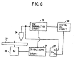
- FIG.6 shows a block diagram of an example of a CD-R recording servo system, to which the servo circuit of the embodiment of the present invention can be applied.
- an optical disk 20 (recording medium) is rotated by a spindle motor 22.
- An optical pickup 24 reproduces a wobble signal shown in FIG.7B from the disk 20, and outputs a WBL signal shown in FIG.7C.
- the WBL signal shown in FIG.7C is obtained from converting the wobble signal shown in FIG.7B into a two-level signal.
- the WBL signal is supplied to an FSK demodulation circuit 26, and a BIDATA signal shown in FIG.7A is obtained from the demodulation. Further, a synchronization signal (ATIP syc ) is detected.
- the BIDATA signal is supplied to a digital PLL circuit 30.
- the digital PLL circuit 30 generates a clock signal which is in synchronization with the BIDATA signal and supplies the clock signal to a switch 32.
- the switch 32 selects the reproduced WBL signal when rotation of the disk 20 is started. When the rotation of the disk 20 is stabilized, the switch 32 selects the clock signal, output by the digital PLL circuit 30, and supplies the selected signal to a spindle servo circuit 34.
- the spindle servo circuit 34 based on the signal obtained from performing 1/3.5 frequency dividing on the WBL signal, or the clock signal, supplied by the switch 32, and the synchronization signal from the FSK demodulation circuit 36, controls the rotation speed of the spindle motor 22 so that the line velocity of the disk 20 becomes constant.
- FIG.8 shows a block diagram of the spindle servo circuit in the first embodiment of the present invention.
- the clock signal PLLCLK, output by the digital PLL circuit 30 is input to a terminal 40, and is supplied to an edge detector (EDG) 42.
- This clock signal is of the frequency 6.3 kHz when the operation speed is the single speed, is of the frequency 12.6 kHz when the operation speed is the double speed, and is of the frequency 25.2 kHz when the operation speed is the four-times speed.
- the edge detector 42 generates pulses resulting from detecting the rising edges of the clock signal.
- a counter 44 when an edge detection pulse is supplied, the value supplied by an adder 46 is loaded. Then, the counter 44 counts system clock pulses CLK supplied via a terminal 48.
- the output value of the adder 46 is ordinarily a reference value, -1371.
- the system clock pulses CLK are of a frequency 8.64 MHz when the operation speed is the single speed, are of a frequency 17.29 MHz when the operation speed is the double speed and are of a frequency 34.57 MHz when the operation speed is the four-times speed.
- the counter 44 each time an edge detection pulse is input, outputs a count value 0 if the clock signal PLLCLK includes no speed error, outputs a negative count value if the clock signal PLLCLK is faster and outputs a positive count value if the clock signal PLLCLK is slower.
- the counter 44 outputs the count value depending on the speed error of the PLLCLK.
- the count value is supplied to a register (REG) 50, and is stored therein each time an edge detection pulse is input.
- An averaging circuit 52 averages the count value stored in the register 50 and a predetermined number of preceding count values. Then, the resulting value is supplied to an over-sampling circuit (OVS) 54.
- OVS over-sampling circuit
- a frequency multiplication circuit 56 performs frequency multiplication by 4 on edge detection pulses and supplies the resulting clock signal to the over-sampling circuit 54.
- the over-sampling circuit 54 uses the clock signal to perform over-sampling on the output of the averaging circuit 52.
- approximately 1/4 the output of the averaging circuit 52 is obtained, and is supplied to an adder 58.
- the adder 58 adds an offset value 172 to the over-sampling output, and supplies the resulting value to a PWM (Pulse Width Modulation) circuit 60.
- the offset value 172 corresponds to the 50% duty of each period of the clock pulses obtained from performing the frequency multiplication by 4.
- the PWM circuit 60 is reset by each clock pulse output by the frequency multiplication circuit 56, and counts the system clock pulses CLK which are supplied via a terminal 62.
- the PWM circuit 60 generates a rectangular wave signal, as a speed error signal, such that the signal becomes a high level (+5 V) until the count value becomes equal to the output value of the adder 58 from 0 and then becomes a low level (0 V), and supplies the rectangular wave signal to an addition circuit 64.
- the counter 44 and the register 50 act as the speed error detecting means M1 shown in FIGS.5A and 5B.
- a reference value 676 and the output of a register (REG) 72 are supplied to an adder 70.
- the adders 70 adds these values, and supplies the resulting value to a counter 74.
- the output value of the register 72 is initially reset to 0.
- the counter 74 is an 11-bit counter, and performs feedback of each carry, output by itself, to the loading terminal thereof.
- the output value of the adder 70 is loaded in the carry output timing, and counts the system clock pulses CLK supplied via a terminal 76.
- the counter 74 outputs a carry each time 1372 system clock pulses are input after 676 is loaded, and thus, the counter 74 runs by itself.
- the carries are of a frequency 6.3 kHz when the operation speed is the single speed, and are supplied, as a reference signal Tref, to an edge detector (EDG) 78 and a frequency multiplication circuit 80.
- the edge detector 78 detects the rising edges of the reference signal Tref, and supplies the detection result to a register 92.
- the clock signal PLLCLK is supplied to an edge detector 82 via a terminal 81.
- the edge detector 82 detects the rising edges of the clock signal PLLCLK, and supplies the detection result to a counter 88 and a register 90.
- the counter 86 counts the system clock pulses CLK supplied via a terminal 84, and supplies the count value to the register 90.
- the register 90 stores the count value at each rising edge of the clock signal PLLCLK.
- the counter 88 After being reset by each rising edge of the clock signal PLLCLK, the counter 88 counts the system clock pulses CLK supplied via the terminal 84, and supplies the count value to the register 92.
- the register 92 stores the count value at each rising edge of the reference signal Tref.
- the register 90 stores the system clock pulse count value for the period A
- the register 92 stores the system clock pulse count value for the period B.
- a subtracter 94 subtracts the output value of the register 92 from the output value of the register 90, thus obtains a phase error amount A-B and supplies this amount to an averaging circuit 96.
- the averaging circuit 96 averages the supplied amount and a predetermined number of preceding phase error amounts.
- the averaging circuit 96 supplies the absolute value of the average to a PWM circuit 98 and supplies the sign of the average to the input terminal of a tristate buffer 100.
- the PWM circuit 98 is reset by clock pulses which are obtained by performing frequency multiplication by 4 on the reference signal Tref through the frequency multiplication circuit 80, and counts the system clock pulses CLK supplied via a terminal 102.
- the PWM circuit 98 generates a rectangular wave signal such that the level of the signal is low until the count value becomes the output value of the averaging circuit 96 from 0, and then, the level of the signal becomes high, and supplies the rectangular wave signal to the control terminal of the tristate buffer 100.
- the tristate buffer 100 is in an output state when the rectangular wave signal output by the PWM circuit 98 is at the low level, outputs a +5-V signal if the sign supplied by the averaging circuit 96 is positive and outputs a 0-V signal if the sign is negative.
- the tristate buffer 100 is in a high impedance state when the above-mentioned rectangular wave signal is at the high level. Therefore, when the duration A is equal to the duration B, the tristate buffer is in the high impedance state; when the duration A is longer than the duration B, the tristate buffer 100 outputs +5 V; and when the duration B is longer than the duration A, the tristate buffer 100 outputs 0 V.
- the tristate buffer 100 generates such a phase error signal and supplies the signal to the addition circuit 64.
- the addition circuit 64 includes a built-in . low-pass filter, and performs addition of analog voltages.
- the speed error signal of 0 V and 5 V is integrated by the low-pass filter and a DC value is obtained.
- the phase error signal of 0 V, 5 V and high impedance is integrated by the low-pass filter in which, for example, 2.5 V is taken for the high impedance state. Thus, a DC value is obtained.
- the addition circuit 64 adds the DC values of the speed error signal and the phase error signal, and outputs a signal of the resulting value as a servo signal via a terminal 104 to the spindle motor 22 shown in FIG.6.
- the above-mentioned counters 74, 86, 88 and subtracter 94 act as the phase error detecting means M2, and the averaging circuit 52, OVS 54, adder 58, PWM circuit 60, averaging circuit 96, PWM circuit 98, tristate buffer 100 and adder 64 act as the servo signal generating means M3, shown in FIGS.5A and 5B.
- the portion of the servo circuit for performing a servo operation so that the frequency (speed) and the phase of the clock signal PLLCLK which is obtained from the BIDATA signal reproduced from the optical disk may be equal to and may be in synchronization with the frequency (speed) and the phase of the reference signal Tref which is generated from the system clock pulses CLK, respectively.
- a portion of the servo circuit which will now be described, performs a servo operation so that the phase of the synchronization signal (ATIP syc ) of a frequency of approximately 75 Hz reproduced from the optical disk 20 may be in synchronization with the phase of the synchronization signal (SBSY: sub-code sync) of a frequency of 75 Hz included in recording data.
- the phase of the synchronization signal (ATIP syc ) of a frequency of approximately 75 Hz reproduced from the optical disk 20 may be in synchronization with the phase of the synchronization signal (SBSY: sub-code sync) of a frequency of 75 Hz included in recording data.
- the synchronization signal SBSY of recording data is supplied to a terminal 110, and an edge detector 112 detects the rising edges of the signal SBSY and supplies the detection result to a phase difference detector 114.
- the synchronization signal ATIP syc reproduced from the optical disk is supplied to a terminal 116, and an edge detector 118 detects the rising edges of the signal ATIP syc and supplies the detection result to the phase difference detector 114, a register 120 and a delay circuit 122.
- a frequency divider 126 performs 1/4 frequency dividing on the system clock pulses CLK supplied via a terminal 124, and supplies the resulting clock pulses to the phase difference detector 114 and the register 120.
- phase difference detector 0 is loaded in the phase difference detector 114 at the time of each rising edge of the synchronization signal SBSY (or ATIP syc ), and then, the phase difference detector 114 counts the 1/4 frequency divided system clock pulses until the time of the subsequent rising edge of the synchronization signal ATIP syc (or SBSY). Thus, the phase difference is detected as the count value.
- the count value is supplied to the register 120. The count value is positive when the ATIP syc is later, and the count value is negative when the SBSY is later.
- the register 120 stores the count value of the phase difference supplied at the time of the rising edge of the synchronization signal ATIP syc (or SBSY), and supplies the count value to a comparator 128 and the register 72.
- the value ⁇ 343 corresponding to one period of the clock signal PLLCLK is supplied to the comparator 128.
- the comparator 128 supplies a trigger signal and the sign of phase-difference count value to a data generator 130.
- the comparator 128 supplies a trigger signal and the sign of the phase-difference count value to the register 72.
- the register 72 To the register 72, the count value output by the register 120 is supplied, and also, a signal obtained from delaying the output of the edge detector 118 through the delay circuit 122 is supplied. Further, a microprocessor (not shown in the figure) which controls the entire device supplies an enable signal EN to a terminal 132. The register 72 outputs 0 when the trigger signal is supplied if the enable signal EN is not supplied. If the enable signal EN is supplied, the register 72, when the trigger signal is supplied by the comparator 128, stores the output of the register 120, and outputs it.
- the phase difference detector 114 when the phase difference is equal to or smaller than one period of the clock signal PLLCLK, the phase-difference count value counted by the phase difference detector 114 is supplied to the adder 70, and is added to the reference value. Thereby, the generation timing of the reference signal Tref varies for performing a servo operation so that the synchronization signal ATIP syc is in synchronization with the synchronization signal SBSY.
- the enable signal EN is supplied via a terminal 134. If the enable signal EN is not supplied, the data generator 130 generates 0 when the trigger signal is supplied by the comparator 128. When the enable signal EN is supplied, the data generator 130 generates a predetermined value, ⁇ N from the trigger signal and the sign supplied by the comparator 128, and supplies the ⁇ N to the adder 46.
- the sign of the ⁇ N is the sign supplied by the comparator 128, and N is a value which was previously written by the microprocessor. For example, N is any one of 2, 3, 4.
- the data generator 130 when the phase difference is larger than one period of the PLLCLK, the data generator 130 generates the predetermined value ⁇ N, and the ⁇ N is added to the reference value, -1371, in the adder 46. Thereby, the value loaded in the counter 44 varies for performing a servo operation so that the synchronization signal ATIP syc is in synchronization with the synchronization signal SBSY.
- phase difference detector 114 and register 120 act as the second phase error detecting means M4, shown in FIGS.5A and 5B, and the register 72 and adder 70 act as the reference phase changing means M5.
- the data generator 130 and adder 46 act as the reference frequency changing means M6.
- phase difference of the ATIP syc when the phase difference of the ATIP syc is equal to or smaller than one period of the PLLCLK, a large value, between -343 and +343, is added to the adder 70 of the phase error system.
- a small value, ⁇ 2, ⁇ 3, or ⁇ 4 is added to the adder 46 of the speed error system. This is because, generally speaking, the loop gain of such a speed error system is several times to hundreds of times the loop gain of such a phase error system. Accordingly, a feedback amount to the speed error system may be smaller than a feedback amount to the phase error system.
- the above-mentioned microprocessor when the device starts, causes the switch 32, shown in FIG.6, to select the WBL signal, and, when the rotation of the disk 20 is stabilized, causes the switch 32 to select the clock signal PLLCLK. At this time, the microprocessor does not supply the enable signal EN to the terminals 132 and 134, shown in FIG.8. In the recording mode, after the clock signal PLLCLK comes to be in synchronization with the reference signal Tref, the microprocessor supplies the enable signal to the terminals 132 and 134, and causes the synchronization signal ATIP syc to be in synchronization with the synchronization signal SBSY.
- the speed error detecting means detects the speed error which is the difference in frequency between the reproduced clock signal reproduced from the recording medium and the reference clock signal.
- the first phase error detecting means detects the phase error which is the difference in phase between the reproduced clock signal and the reference clock signal.
- the servo signal generating means generates the servo signal which is used for eliminating the above-mentioned speed error and phase error.
- the second phase error detecting means detects the phase error which is a phase difference between the synchronization signal reproduced from the recording medium separately from the above-mentioned reproduced clock signal and the reference synchronization signal.
- the reference phase changing means changes the phase of the reference clock signal based on the phase error detected by the second phase error detecting means.
- the phase of the reference clock signal which is used for detecting the phase error of the reproduced clock signal, is changed based on the phase error of the reproduced synchronization signal reproduced from the recording medium.
- the time required for correcting the phase error of the reproduced synchronization signal can be reduced.
- the stabilized reproduced clock signal and reproduced synchronization signal can be reproduced earlier.
- the speed error signal which is the rectangular wave of the pulse width corresponding to the speed error
- the phase error signal which is the rectangular wave of the pulse width corresponding to the phase error
- the phase error loop gain should also be changed from a single amount, to a four-times amount and to a sixteen-times amount.
- the multiplication rate of the speed error loop gain should be the same as the multiplication rate of the phase error loop gain.
- the two registers for holding the count values of the two counters, respectively, the subtracter, and the pulse width modulation circuit for changing the duty ratio of the phase error signal using the output of the subtracter should be provided.
- the circuit scale is large.
- the speed error detecting means detects the speed error which is the difference in frequency between the reproduced clock signal reproduced from the recording medium and the reference clock signal.
- the phase error detecting means detects the phase error which is the difference in phase between the reproduced clock signal and the reference clock signal.
- the servo signal generating means generates the servo signal which is used for eliminating the above-mentioned speed error and phase error.
- the phase error detecting means comprises first and second frequency dividing means and phase comparing means. The first and second frequency dividing means perform frequency dividing on the reproduced clock signal and the reference clock signal, respectively.
- the frequency dividing ratio is changed according to a change of the speed error gain of the speed error detecting means.
- the phase comparing means detects the phase error between the frequency-divided reproduced clock signal and the frequency-divided reference clock signal. This is the subject of get another divisional application.
- the frequency dividing ratio of the reproduced clock signal and the reference clock signal is changed according to a change of the speed error gain.
- the phase error detecting period is changed.
- the phase error gain is changed according to the speed error gain, and the pulse width modulation circuit and so forth are not needed.
- the circuit arrangement can be simpler and the circuit scale can be reduced.
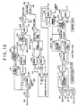
- FIG.10 shows a block diagram of the spindle servo circuit.
- the reproduced clock signal PLLCLK reproduced from the recording medium and output by the digital PLL circuit 30, shown in FIG.6, is input to a terminal 1040, and is supplied to an edge detector (EDG) 1042.
- This clock signal is of the frequency 6.3 kHz when the operation speed is the single speed, is of the frequency 12.6 kHz when the operation speed is the double speed, and is of the frequency 25.2 kHz when the operation speed is the four-times speed.
- the edge detector 1042 generates pulses resulting from detecting the rising edges of the clock signal.
- a counter 1044 when an edge detection pulse is supplied, a reference value -1371 is loaded. Then, the counter 1044 counts system clock pulses CLK supplied via a terminal 1048.
- the system clock pulses CLK are of a frequency 8.64 MHz when the operation speed is the single speed, are of a frequency 17.29 MHz when the operation speed is the double speed and are of a frequency 34.57 MHz when the operation speed is the four-times speed. Therefore, the counter 1044, each time an edge detection pulse is input, outputs a count value 0 if the clock signal PLLCLK includes no speed error, outputs a negative count value if the clock signal PLLCLK is faster and outputs a positive count value if the clock signal PLLCLK is slower. Thus, the counter 1044 outputs the count value depending on the speed error of the PLLCLK.
- the count value is supplied to a register (REG) 1050, and is stored therein each time an edge detection pulse is input.
- An averaging circuit 1052 averages the count value stored in the register 1050 and a predetermined number of preceding count values. Then, the resulting value is supplied to an over-sampling circuit (OVS) 1054.
- OVS over-sampling circuit
- the edge detection pulses are caused to be in synchronization with the system clock pulses, and then are supplied to a frequency multiplication circuit 1056.
- the frequency multiplication circuit 1056 performs frequency multiplication by 4 on the edge detection pulses.
- the clock pulses obtained from performing the frequency multiplication by 4 on the edge detection pulses through the frequency multiplication circuit 1056 are supplied to the over-sampling circuit 1054.
- the over-sampling circuit 1054 uses the clock pulses, the over-sampling circuit 1054 performs over-sampling on the output of the averaging circuit 1052.
- approximately 1/4 of the output of the averaging circuit 1052 is obtained, and is supplied to a speed gain circuit 1057. (Because sampling is performed using four-times frequency clock pulses, it is necessary to make each value to be sampled be 1/4 of the original value.)
- Gain data is supplied to the speed gain circuit 1057 via a terminal 1055 from a microprocessor (not shown in the figure).
- the gain data indicates, for example, a frequency dividing ratio 1/16 when the operation speed is the single speed, a frequency dividing ratio 1/4 when the operation speed is the double speed, and a frequency dividing ratio 1 when the operation speed is the four-times speed.
- the speed gain circuit 1057 multiplies the value supplied by the over-sampling circuit 1054 by the above-mentioned gain data, and supplies the resulting value to an adder 1058.
- the adder 1058 adds an offset value 172 to the over-sampling output, and supplies the resulting value to a PWM (Pulse Width Modulation) circuit 1060.
- the offset value 172 corresponds to the 50% duty of each period of the clock pulses obtained from performing the frequency multiplication by 4.
- the PWM circuit 1060 is reset by each clock pulse output by the frequency multiplication circuit 1056, and counts the system clock pulses CLK which are supplied via a terminal 1062.
- the PWM circuit 1060 generates a rectangular wave signal, as a speed error signal, such that the signal is at a high level (+5 V) until the count value becomes equal to the output value of the adder 1058 from 0 and then becomes a low level (0 V), and supplies the rectangular wave signal to an addition circuit 1064.
- the counter 1044 and the register 1050 act as the speed error detecting means.
- a reference value 676 and the output of an adding value control circuit 1072 are supplied to an adder 1070.
- the adder 1070 adds these values, and supplies the resulting value to a counter 1074.
- the output value of the adding value control circuit 1072 is initially reset to 0.
- the counter 1074 is an 11-bit counter, and performs feedback of each carry, output by itself, to the loading terminal thereof.
- the output value of the adder 1070 is loaded in the carry output timing, and counts the system clock pulses CLK supplied via a terminal 1076.
- the counter 1074 outputs a carry each time 1372 system clock pulses are input after 676 is loaded, and thus, the counter 1074 runs by itself.
- the carries are of a frequency 6.3 kHz when the operation speed is the single speed, and are supplied, as a reference signal (reference clock signal) Tref, to a counter 1078.
- the counter 1078 acting as the first frequency dividing means, is in synchronization with the system clock pulses CLK supplied via a terminal 1080.
- the counter 1078 performs frequency dividing on the reference signal Tref according to the instructions of frequency dividing data supplied via a terminal 1082, and outputs a signal REF.
- the counter 1078 performs 1/16 frequency dividing on the reference signal Tref and outputs the signal REF such that the signal has the value 0 during eight periods of the Tref and the signal has the value 1 during the subsequent eight periods of the Tref.
- the counter 1078 When the operation speed is the double speed, the counter 1078 performs 1/4 frequency dividing on the reference signal Tref and outputs the signal REF such that the signal has the value 0 during two periods of the Tref and the signal has the value 1 during the subsequent two periods of the Tref.
- the counter 1078 When the operation speed is the four-times speed, the counter 1078 performs 1/1 frequency dividing on the reference signal Tref. In this case, the counter 1078 does not perform frequency dividing and the signal REF is equal to the reference signal Tref.
- a counter 1084 acting as the second frequency dividing means, is in synchronization with the system clock pulses CLK. The counter 1084, according to the frequency dividing data, performs frequency dividing on the clock signal (reproduced clock signal) PLLCLK and outputs a signal DBCK.
- the signal REF output by the counter 1078 is supplied to a terminal S of a phase comparator 1092, and the signal DBCK output by the counter 1084 is supplied to a terminal R of the phase comparator 1092.
- the phase comparator 1092 acting as the phase comparing means, includes an SR flip-flop and an exclusive-OR circuit.
- the Q output of the flip-flop which is set at the time of each rising edge of the signal REF and is reset at the time of each rising edge of the signal DBCK, is supplied to a tristate buffer 1094 as phase data.
- the output of the exclusive OR when each of the signal REF and the signal DBCK rises is supplied to the control terminal of the tristate buffer 1094, as an enable signal.
- the enable signal is at a low level when the output of the exclusive OR is 1 and the enable signal is at a high level when the output of the exclusive OR is 0.
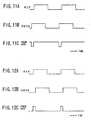
- the phase data shown in FIG.11C is obtained.
- the signals REF and DBCK are such as those shown in FIGS.12A and 12B, respectively, for example, the phase data shown in FIG.12C is obtained.
- the tristate buffer 1094 is in the output state when the enable signal is at the low level, and is in the high impedance state when the enable signal is at the high level.
- the phase data is such as that shown in FIG.11C, only the low-level phase data is supplied to the addition circuit 1064 from the tristate buffer 1094, as a phase error signal.
- phase data is such as that shown in FIG.12C
- only the high-level phase data is supplied to the addition circuit 1064 from the tristate buffer 1094, as the phase error signal.
- the output voltage of the tristate buffer 1064 is 5 V for the high level and is 0 V for the low level.
- the frequency dividing ratio of the reproduced clock signal and the reference clock signal is changed according to the frequency dividing data, simultaneously with a change of the speed error gain according to the gain data corresponding to the frequency dividing data.
- the phase error detecting period is changed.
- the phase error gain is changed according to the change of the speed error gain, and the pulse width modulation circuit and so forth provided in the embodiment of the invention are not needed.
- the circuit arrangement can be simpler and the circuit scale can be reduced.
- the addition circuit 1064 includes a built-in low-pass filter, and performs addition of analog voltages.
- the speed error signal of 0 V and 5 V supplied by the PWM circuit 1060 is integrated by the low-pass filter and a DC value is obtained.
- the phase error signal of 0 V, 5 V and high impedance supplied by the tristate buffer 1094 is integrated by the low pass filter in which, for example, 2.5V is taken for the high impedance state. Thus, a DC value is obtained.
- the addition circuit 1064 adds the DC values of the speed error signal and the phase error signal, and outputs a signal of the resulting value as a servo signal via a terminal 1096 to the spindle motor 22 shown in FIG.6.
- the above-mentioned counters 1078, 1084, and the phase comparator 1092 act as the phase error detecting means, and the averaging circuit 1052, OVS 1054, speed gain circuit 1057, adder 1058, PWM circuit 1060, tristate buffer 1094 and adder 1064 act as the servo signal generating means.
- the portion of the servo circuit for performing a servo operation so that the frequency (speed) and the phase of the clock signal PLLCLK which is obtained from the BIDATA signal reproduced from the optical disk may be equal to and may be in synchronization with the frequency (speed) and the phase of the reference signal Tref which is generated from the system clock pulses CLK, respectively.
- the portion of the servo circuit which will now be described, performs a servo operation so that the phase of the synchronization signal (ATIP syc ) of a frequency of approximately 75 Hz reproduced from the optical disk 20 may be in synchronization with the phase of the synchronization signal (SBSY: sub-code sync) of a frequency of 75 Hz included in recording data.
- the phase of the synchronization signal (ATIP syc ) of a frequency of approximately 75 Hz reproduced from the optical disk 20 may be in synchronization with the phase of the synchronization signal (SBSY: sub-code sync) of a frequency of 75 Hz included in recording data.
- the synchronization signal SBSY of recording data is supplied to a terminal 1110, and an edge detector 1112 detects the rising edges of the signal SBSY and supplies the detection result to a phase difference detector 1114.
- the synchronization signal ATIP syc reproduced from the optical disk is supplied to a terminal 1116, and an edge detector 1118 detects the rising edges of the signal ATIP syc and supplies the detection result to the phase difference detector 1114 and a register 1120.
- a frequency divider 1126 performs 1/4 frequency dividing on the system clock pulses CLK supplied via a terminal 1124, and supplies the resulting clock pulses to the phase difference detector 1114 and the register 1120.
- phase difference detector 1114 is loaded in the phase difference detector 1114 at the time of each rising edge of the synchronization signal SBSY (or ATIP syc ), and then, the phase difference detector 1114 counts the 1/4 frequency divided system clock pulses until the time of the subsequent rising edge of the synchronization signal ATIP syc (or SBSY). Thus, the phase difference is detected as the count value.
- the count value is supplied to the register 1120. The count value is positive when the ATIP syc is later, and the count value is negative when the SBSY is later.
- the register 1120 stores the count value of the phase difference supplied at the time of each rising edge of the synchronization signal ATIP syc (or SBSY), and supplies the count value to a comparator 1128 and an ATIP phase gain circuit 1132.
- the comparing value ⁇ 343 corresponding to one period of the clock signal PLLCLK is supplied to the comparator 1128.
- the comparator 1128 supplies a flag signal to a selection circuit 1134 and the adding value control circuit 1072.
- the flag signal indicates ON when the above-mentioned count value is less than -343 or more than +343, that is, when the phase difference is larger than one period of the clock signal PLLCLK.
- the flag signal indicates OFF when the above-mentioned count value is equal to or more than -343 and less than or equal to +343.
- the comparator 1128 supplies a trigger signal to the ATIP phase gain circuit 1132.
- the selection circuit 1134 selects phase shifting data set in a register 1130 when the phase difference is larger than one period of the clock signal PLLCLK and the ON flag signal is supplied.
- the selection circuit 1134 selects the phase error data output by the ATIP phase gain circuit 1132 when the OFF flag signal is supplied.
- the selection circuit 1134 supplies the selected data to the adding value control circuit 1072.
- the phase shifting data for shifting phase at high speed is set by the microprocessor.
- the phase shifting data is, for example, approximately 80 when the operation speed is the single speed, and approximately 40 when the operation speed is the double speed.
- the ATIP phase gain circuit 1132 When the trigger signal is supplied by the comparator 1128, the ATIP phase gain circuit 1132 generates the phase error data as a result of multiplying the phase-difference count value, supplied by the register 1120, by a predetermined gain (positive value less than 1, or 0). Selection of one of the positive value less than 1 and 0 is performed according to instructions by the microprocessor. The generated phase error data is supplied to the selection circuit 1134. Ordinarily, the maximum value of the phase error data is less than the phase shifting data.
- the frequency dividing data is supplied to the adding value control circuit 1072 via a terminal 1136.
- the flag signal is supplied to the adding value control circuit 1072 from the comparator 1128.
- the adding value control circuit 1072 when the frequency dividing data specifies 1/N frequency dividing, supplies the phase shifting data or the phase error data, supplied by the selection circuit 1134, to the adder 1070 once per N periods of the reference signal Tref.
- the adding value control circuit 1072 controls the adding value to be supplied to the adder 1070.
- the gain of the ATIP phase gain circuit 1132 is selected to be 0 by the microprocessor, after the flag signal indicates OFF, during 64 periods of the reference signal Tref, the gain of the ATIP phase gain circuit 1132 is automatically selected by the microprocessor to be the positive value less than 1. After the 64 periods have elapsed, the gain of the ATIP phase gain circuit 1132 is selected to be 0. This is because, if the phase error data is 0 immediately after the flag signal indicates OFF, phase control is stopped and a state where the rising edges of the ATIP syc are not in synchronization with the rising edges of the SBSY may occur, which should be prevented.
- the generation timing of the reference signal Tref is changed.
- a servo operation is performed so that the synchronization signal ATIP syc may be in synchronization with the synchronization signal SBSY.
- the microprocessor causes the switch 32, shown in FIG.6, to select the WBL signal when the device starts, and then, causes the switch 32 to select the clock signal PLLCLK when the rotation of the optical disk 20 is stabilized.
- the microprocessor gives instructions that the phase control of the synchronization signal ATIP syc and the synchronization signal SBSY is to be performed, the phase control of the synchronization signal ATIP syc and the synchronization signal SBSY is performed and phase control of the signal REF and the signal DBCK is performed simultaneously.
- the synchronization signal ATIP syc is in synchronization with the synchronization signal SBSY.
- the microprocessor gives instructions that the phase.
- the phase control of the synchronization signal ATIP syc and the synchronization signal SBSY is not performed. Then, when the microprocessor gives instructions that the phase control of the synchronization signal ATIP syc and the synchronization signal SBSY is to be performed, the phase control of the synchronization signal ATIP syc and the synchronization signal SBSY is performed, and thereby, the synchronization signal ATIP syc is in synchronization with the synchronization signal SBSY.
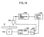
- FIG.13 shows a block diagram of an example of a CD-R recording servo system, to which a digital PLL circuit, which will be described later, can be applied.
- an optical disk 20 is rotated by a spindle motor 2022.
- An optical pickup 2024 reproduces a wobble signal shown in FIG.7B from the disk 20, and outputs a WBL signal shown in FIG.7C.
- the WBL signal shown in FIG.7C is obtained from converting the wobble signal shown in FIG.7B into a two-level signal.
- the WBL signal is supplied to an FSK demodulation circuit 2026, and a BIDATA signal shown in FIG.7A is obtained from the demodulation.
- the BIDATA signal is supplied to the digital PLL circuit 2030.
- the digital PLL circuit 2030 generates a clock signal which is in synchronization with the BIDATA signal and supplies the clock signal to a switch 2032.
- the switch 2032 selects the reproduced WBL signal when rotation of the disk 20 is started. When the rotation of the disk 20 is stabilized, the switch 2032 selects the clock signal, output by the digital PLL circuit 2030, and supplies the selected signal to a spindle servo circuit 2034.
- the spindle servo circuit 2034 based on the signal obtained from performing 1/3.5 frequency dividing on the WBL signal, or the clock signal, supplied by the switch 2032, controls the rotation speed of the spindle motor 2022 so that the line velocity of the disk 20 becomes constant.
- FIG.14 shows a block diagram of the digital PLL circuit 2030.
- a BIDATA signal such as that shown in FIG.3A
- the edge counter 2042 acting as the measuring means, is reset at the rising edges and the decaying edges, and counts system clock pulses which are input via a terminal 2044.
- the edge counter measures the edge durations of the BIDATA signal and outputs them.
- the frequency of the system clock pulses is changed from the single-speed frequency, to double the single-speed frequency and to four times the single-speed frequency as the operation speed of the disk 20 is changed from the single speed, to the double speed and to the four-times speed.
- the number of system pulses during the pulse width 1T of the BIDATA signal is 686 as a standard.
- the count value of the edge counter 2042 for the pulse width 1T is 686
- the count value for the pulse width 2T is 1372
- the count value for the pulse width 3T is 2058.
- a 1T generating circuit 2046 determines whether or nor the count value, supplied by the edge counter 2042 immediately before the count value becomes 0, that is, the maximum count value, is within the range of 686 ⁇ (where ⁇ is a value on the order of 10) or within the range of 1372 ⁇ 2 ⁇ . When the maximum count value is in the range of 686 ⁇ , the maximum count value is held as the value of 1T. When the maximum count value is in the range of 1372 ⁇ 2 ⁇ , 1/2 of the maximum count value is held as the value of 1T.
- the iT generating circuit 2046 detects the pulse widths 1T, 2T of the BIDATA signal, generates the value of iT, and ignores the pulse width 3T of the BIDATA signal.
- the value of 1T near the value 686, output by the 1T generating circuit is supplied to an adder 2048 and to a multiplier 2050.
- the adder 2048 adds the fixed value -343, supplied by a fixed-value generator 2052, to the value of 1T in order to reduce the number of bits.
- the added result is supplied to a digital low-pass filter 2054.
- the digital low-pass filter 2054 removes sharp fluctuation components of the supplied value, and supplies the resulting value to an adder 2056.
- the adder 2056 adds the fixed value 343, supplied by a fixed-value generator 2058, to the supplied value. Thus, the value 1T is obtained.
- the value 1T is supplied to an adder 2060.
- the adder 2060 adds a phase error correction value to the supplied value.
- the corrected value of 1T is supplied to an NCO (Numerically Controlled Oscillator) 2062.
- NCO Numerically Controlled Oscillator
- the system clock pulses are supplied to the NCO 2062 via a terminal 1064.
- the NCO counts the system clock pulses and generates the clock signal shown in FIG.3B which rises when the count value of the system clock pulses becomes the value of 1T from the adder 2060, and resets the count value.
- the clock signal is output via a terminal 2066, and also, is supplied to a latch circuit 2068.
- the above-mentioned 1T generating circuit 2046 and the adder 2048 to the NCO 2062 act as the clock generating means.
- the count value output by the edge counter 2042 is supplied to the latch circuit 2068.
- the latch circuit 2068 holds the supplied count value at each rising of the clock signal supplied by the NCO 2062, and supplies the held count value to a subtracter 2070.
- the latch circuit 2068, to which the BIDATA signal is also supplied holds the count value at only the first rising of the clock signal from the starting edge of each of the pulse widths 1T, 2T and 3T of the BIDATA signal, and does not hold the count value at second (in the case of 2T, 3T) nor third (in the case of 3T) rising, in the same pulse width, of the clock signal.
- the subtracter 2070 To the subtracter 2070, the value obtained from multiplying the value of 1T, output by the 1T generating circuit 2046, by 1/2 through the multiplier 2050 is supplied, as a reference value.
- the subtracter 2070 subtracts the reference value from the value output by the latch circuit 2068, and thus obtains a phase error value.
- the phase error value is supplied to an integrator 2072.
- 1/2 of the value of 1T is used as the reference value is that, as shown in FIGS.3A, 3B, rising of the clock signal is positioned at the center of each pulse width 1T.
- the integrator 2072 performs proportional integration on the phase error value.
- the integrated value is multiplied by 1/K (where K is a real number equal to or more than 1) through a multiplier 2074.
- K is a real number equal to or more than 1
- the multiplier 2050, latch circuit 2068 to multiplier 2074 and adder 2060 act as the phase correcting means.
- the 1T generating circuit 2046 generates the value of 1T only from the pulse widths iT and 2T of the BIDATA signal, and does not use the pulse width 3T of the BIDATA signal.
- the repeating frequency 75 Hz (in the single speed) synchronization signal (ATIP syc ) in the BIDATA signal is of the pattern of 3T, 1T, 1T and 3T as shown in FIG.3A. Because the 1T generating circuit 2046 does not use the 3T pattern, there is no possibility that a 75-Hz component of the synchronization signal is mixed into the output value of the 1T generating circuit 2046. Thereby, stabilization of the clock signal is improved.
- the entirety of the digital PLL circuit is formed of a digital circuit. Accordingly, the operation is stable against ambient temperature and power supply voltage fluctuation in comparison to an analog circuit. Further, when the circuit is formed to be an integrated circuit, no externally connected circuit is required.
- the circuit only by changing the frequency of the system clock pulses supplied via the terminals 2044 and 2064, it is possible to configure the circuit for the operation speed, the single speed, double speed and four-times speed. Further, the circuit operates based on the count value of the edge counter 2042, linearity is good and the capture range of the phase locking operation is wider.
- the 1T generating circuit generates the value of iT from the detected values of the pulse widths 1T and 2T of the BIDATA signal. However, it is also possible that the 1T generating circuit generates the value of 1T only from the detected values of the pulse width 1T of the BIDATA signal.
- FIG.15 shows a block diagram of an optical disk device.
- an optical disk 20 is rotated by a spindle motor 3022.
- An optical pickup 3024 reproduces a wobble signal shown in FIG.7B from the disk 20, and outputs a WBL signal shown in FIG.7C.
- the WBL signal shown in FIG.7C is obtained from converting the wobble signal shown in FIG.7B into a two-level signal.
- the WBL signal is supplied to a digital FSK demodulation circuit 3026, and a BIDATA signal shown in FIG.7A is obtained from the demodulation. Further, the synchronization signal (ATIP syc ) is detected in the digital FSK demodulation circuit 3026.
- the BIDATA signal is supplied to the digital PLL circuit 3030.
- the digital PLL circuit 3030 generates a clock signal which is in synchronization with the BIDATA signal and supplies the clock signal to a switch 3032.
- the switch 3032 selects the reproduced WBL signal when rotation of the disk 20 is started.
- the switch 3032 selects the clock signal, output by the digital PLL circuit 3030, and supplies the selected signal to a digital spindle servo circuit 3034.
- the digital spindle servo circuit 3034 based on the signal obtained from performing 1/3.5 frequency dividing on the WBL signal, or the clock signal, supplied by the switch 3032, and the synchronization signal, controls the rotation speed of the spindle motor 3022 so that the line velocity of the disk 20 becomes constant.
- All of the digital FSK demodulation circuit 3026, digital PLL circuit 3030, switch 3032 and digital spindle servo circuit 3034 perform digital processing and are formed to be an integrated circuit on a semiconductor chip 3036.
- the WBL signal which is obtained from converting the signal through the optical pickup 3024 into the two-level signal.
- phase angle ⁇ (t) ⁇ c t + ⁇ ⁇ Vs (t) d t + ⁇ .
- the FSK demodulation is to obtain the modulation signal Vs(t) from the instantaneous phase angle ⁇ (t).
- FIG.16 shows a block diagram of an example of the digital FSK demodulation circuit 3026.
- the WBL signal such as that shown in FIG.7C is input to a terminal 3040, and is supplied to an edge detector 3042.
- the frequency of the WBL signal is 22.05 ⁇ 1 kHz when the operation speed is the single speed, is 44.1 ⁇ 2 kHz when the operation speed is the double speed and is 88.2 ⁇ 4 kHz when the operation speed is the four-times speed.
- the frequency of system clock pulses CLK input to a terminal 3044 is 8.64 MHz when the operation speed is the single speed, is 17.29 MHz when the operation speed is the double speed and is 34.57 MHz when the operation speed is the four-times speed.
- the edge detector 3042 detects each rising edge of the WBL signal by using the system clock pulses CLK, and supplies a rising edge detection signal to a counter 3046, a register 3048 and a timing generator 3050.
- the counter 3046 is reset to have the count value of 0, and then, counts the system clock pulses CLK.
- the counter 3046 supplies the count value to the register 3048.
- the register stores the count value when the rising edge detection signal is input.
- the timing generator 3050 generates phase-different timing signals Ta, Tb and timing signals Sa, Sb and Sc in synchronization with the rising edge detection signal of the WBL signal.
- a timing generator 3052 generates timing signals Ta 1 , Tb 1 , Tc 1 , Ta 4 , Tb 4 , Tc 8 , Td 8 , Te 8 .
- the subscripts 'a', 'b', 'c', 'd' represent output timing.
- 'a' represents the earliest timing and 'e' represents the latest timing.
- the subscript '1' represents the frequency 22.05 kHz when the operation speed is the single speed
- the subscript '4' represents the frequency of 88.2 kHz when the operation speed is the single speed
- the subscript '8' represents the frequency of 176.4 kHz when the operation speed is the single speed.
- the count value stored in the register 3048 is 196 ⁇ (where a is on the order of tens) in the ordinary operation.
- This count value is supplied to a comparator 3054 and a multiplexer (MUX) 3056.
- the comparator 3054 outputs a low-level selection signal when the count value of the register 3048 is, for example, within the range of the order of from 100 to 300.
- the comparator 3054 outputs a high-level selection signal when the count value of the register 3048 is out of the range.
- the generated selection signal is supplied to the multiplexer 3056.
- the preceding-time count value, output by a register 3058 is also supplied.
- the multiplexer 3056 selects and outputs the output value (the value obtained at this time) of the register 3048.
- the comparator outputs the high-level selection signal, that is, the count value of the register 3048 is out of the range of the ordinary operation, the multiplexer 3056 selects and outputs the output value (the value obtained at the preceding time) of the register 3058.
- the output value of the multiplexer 3056 is supplied to the register 3058.
- the output of the register 3058 is supplied to a multiplexer 3060 directly and also is supplied the multiplexer 3060 via a register 3062.
- the registers 3058 and 3062 perform storing operations with the different timing signals Ta and Tb, respectively.
- a decoder 3064 decodes the values of the timing signals Sa, Sb and Sc, and determines whether the multiplexer 3060 is caused to select the output value of the register 3058 or the output value of the register 3062.
- the value of the multiplexer 3060 output therefrom according to the determination is stored in a register 3066 in the timing of inputting of the timing signal Tb 4 .
- the stored value is supplied to a digital low-pass filter (LPF) 3068 and a threshold-value generating circuit 3070.
- LPF digital low-pass filter
- the registers 3058, 3062, multiplexer 3060 and decoder 3064 perform timing conversion from the timing in synchronization with the WBL signal to the timing in synchronization with the system clock pulses CLK.
- the digital low-pass filter 3068 removes sudden change components of the supplied count value, and supplies the resulting value to a comparator 3072.
- the threshold-value generating circuit 3070 averages, for example, preceding tens to a hundred and tens of count values, and generates a threshold value which is supplied to an adder 3074. When the optical disk rotates at a predetermined line velocity, the threshold value is a value near 196.
- a hysteresis generator 3076 generates the value of - ⁇ , assuming that the BIDATA signal subsequently comes to be at the low level, when the FSK demodulated output, the BIDATA signal, is at the high level.
- the hysteresis generator 3076 generates the value of + ⁇ , assuming that the BIDATA signal subsequently comes to be at the high level, when the BIDATA signal is at the low level.
- ⁇ is a value on the order of a value less than 10.
- the adder 3074 sets the hysteresis to the above-mentioned threshold value, and supplies the resulting value to the comparator 3072 as a comparison reference value.
- the comparator 3072 compares the output of the digital low-pass filter 3068 with the comparison reference value. Then, a first comparison result of whether or not the former is equal to or more than the latter (when the former is equal to or more than the latter, a high level is output) and a second comparison result of whether or not the former is equal to or less than the latter (when the former is equal to or less than the latter, a low level is output) are supplied to a multiplexer 3080.
- the multiplexer 3080 selects the comparison result, output by the comparator 3072, of whether or not the count value is equal to or less than the threshold value, when the FSK demodulated output, the BIDATA signal, is at the high level.
- the multiplexer 3080 selects the comparison result, output by the comparator 3072, of whether or not the count value is equal to or more than the threshold value when the BIDATA signal is at the low level.
- the selected comparison result is supplied to a D flip-flop 3082.
- the D flip-flop 3082 holds the supplied comparison result with the timing signal Tc 8 , and outputs it via a terminal 3084 as the FSK demodulated output, the BIDATA signal.
- an ATIP syc detection circuit 3086 is connected to the D flip-flop 3082.
- the ATIP syc detection circuit 3086 detects the synchronization signal ATIP syc from the BIDATA signal, and outputs the synchronization signal ATIP syc via a terminal 3088.
- the above-described digital PLL circuit (shown in FIG.14) is used as the digital PLL circuit 3030.
- the above-described spindle servo circuit in the embodiment of the invention (shown in FIG.8) is formed of a digital circuit and is used as the digital spindle servo circuit 3034.
- the addition circuit 64 is an analog circuit. Therefore, this circuit is an externally connected circuit of the semiconductor chip 3036.
- each of the digital FSK demodulation circuit 3026, digital PLL circuit 3030 and digital spindle servo circuit 3034 is a digital circuit and therefore no externally connected circuit is necessary.
- the operation speed is changed from the single speed, to the double speed, and to the four-times speed, it is only necessary to change the frequency of the system clock pulses from the single-speed frequency to double the single-speed frequency and to four times the single-speed frequency. Change of the circuit properties and so forth are not necessary. Thus, it is easy to adapt the device for the different operation speeds.
Description
- The present invention relates to a servo circuit, in particular, to a servo circuit having a speed control system and two phase control systems.
- The present invention also relates to a digital PLL circuit, in particular, to a digital PLL circuit which generates a clock signal which is in synchronization with pulses of predetermined pulse widths included in an input signal.
- The present invention also relates to an optical disk device, in particular, to an optical disk device which performs recording data on a recordable optical disk and reproducing data therefrom.
- US-A-5 170 386, on which the preamble to claim 1 is based, discloses a servo circuit in which the frequency and phase of a reference clock signal is composed to the frequency and phase of a clock signal generated form reproduction of the disc, to provide a spindle speed error signal.
- FIG.1 shows a block diagram of an example of a servo circuit in the related art. In the figure, a speed detected value and a phase detected value are input to
terminals adder 12 subtracts a speed reference value from the speed detected value, and thus, a speed error value is obtained. Amultiplier 13 multiplies the speed error value by a coefficient K1, and then, the product of the multiplication is supplied to anadder 14. Anadder 15 subtracts a phase reference value from the phase detected value, and thus, a phase error value is obtained. Amultiplier 16 multiplies the phase error value by a coefficient K2, and then, the product of the multiplication is supplied to theadder 14. Theadder 14 adds the value supplied from themultiplier 13 to the value supplied from themultiplier 16. Thus, theadder 14 generates a servo error value and outputs it via aterminal 17. - FIG.2 shows a block diagram of an example of an analog PLL (Phase-Locked Loop) circuit in the related art. In the figure, to a
terminal 2010, an input signal including a predetermined frequency component is input, and is supplied to aphase comparator 2011. Thephase comparator 2011 compares the phase of the input signal with the phase of a signal of a predetermined frequency supplied from afrequency divider 2014, and thus, generates a phase error signal. The phase error signal is supplied to a VCO (Voltage-Controlled Oscillator) 2013 through a LPF (Low-Pass Filter) 2012. Thefrequency divider 2014 performs frequency dividing on an oscillated signal outputted from theVCO 2013, and thus, the frequency of the oscillated signal becomes a predetermined frequency. The signal of the predetermined frequency is output via aterminal 2015 and also is supplied to thephase comparator 2011. Thereby, the VCO 2013 generates the oscillated signal which is in synchronization with the predetermined frequency component of the input signal. Thefrequency divider 2014 performs frequency dividing on the oscillated signal, and the resulting signal is output via theterminal 2015. - Only a synchronization signal for disk rotation control and a control signal such as an address signal are previously recorded in a recordable optical disk. As a method therefor, there is a method, as mentioned in the Orange Book which is a standard of a recordable compact disk system (CD-R), in which a groove is formed to meander, and thus, a synchronization signal is recorded on a disk. A signal recorded on a disk in such a way by causing a groove to meander is referred to as a wobble signal.
- The wobble signal is a signal obtained from performing FSK modulation using a bi-phase modulation signal BIDATA which is information such as a disk address and so forth. When disk rotation is of a regular line velocity, the frequency of the wobble signal is 22.05±1 kHz. An ATIP signal, which is the above-mentioned information such as an address and so forth, includes a synchronization signal (ATIPsyc), an address and an error-detecting code CRC. The repeating frequency of the synchronization signal is 75 Hz.
- FIG.3A shows a BIDATA signal obtained from performing FSK demodulation on a wobble signal reproduced from a disk. By supplying the BIDATA signal to the PLL circuit shown in FIG.2, a clock signal such as that shown in FIG.3B is generated. In the BIDATA signal, as shown in FIG.3A, repetition of a
pulse width 1T and a pulse width 2T is an address and CRC pattern. A synchronization signal pattern is, in order to distinguish it from the address and CRC pattern, a pattern ofpulse widths - When data is recorded in the above-mentioned CD-R, speed control and phase control are performed so that the clock signal generated from the BIDATA signal is in synchronization with a reference clock signal. Further, it is also necessary that the phase of a synchronization signal (repeating frequency: 75 Hz) included in recording data is made to be in synchronization with the phase of the synchronization signal (ATIPsyc) of the ATIP signal reproduced from the disk.
- It can be assumed that: a phase error value between the synchronization signal (ATIPsyc) of the ATIP signal and the synchronization signal (SBSY: sub-code sync) of the recording data is obtained; the speed detected value and the phase detected value of the clock signal generated from the BIDATA signal are supplied to the
terminals adder 14 shown in FIG.1. In such a case, there may occur a case where the phase error value of the clock signal is a positive value and the phase error value of the synchronization signals is a negative value. Therefore, a proper servo operation may not be performed. Such a problem will be referred to as a first problem. - The
phase comparator 2011 shown in FIG.2 compares pulse edges of the BIDATA signal shown in FIG.3A with pulse edges of the clock signal shown in FIG.3B. Therefore, the 75 Hz component of the synchronization signal pattern is mixed in the phase error signal, and cannot be removed through theLPF 2012. Thereby, stability of the clock signal is degraded. Such a problem will be referred to as a second problem. - As mentioned above, there is a recordable compact disk system (CD-R) as a system for a recordable disk. In the CD-R, synchronization information for rotation control and address information is recorded as a wobble signal as a result of forming a groove to meander.
- As mentioned above, the wobble signal is a signal obtained from performing FSK modulation using a bi-phase modulation signal BIDATA which is information such as a disk address and so forth. When disk rotation is of a regular line velocity, the frequency of the wobble signal is 22.05±1 kHz. An ATIP signal, which is the above-mentioned information such as an address and so forth, includes a synchronization signal (ATIPsyc), an address and an error-detecting code CRC. The repeating frequency of the synchronization signal is 75 Hz.
- For example, Japanese Laid-Open Patent Application No.5-225580 discloses an optical disk device which performs recording data on such an optical disk and reproducing data therefrom.
- In such an optical disk device, a reproduced signal reproduced through an optical head from an optical disk undergoes signal processing using an analog circuit. Thus, optical disk rotation control is performed.
- A circuit shown in FIG.4 is an example of a demodulation circuit which performs FSK demodulation on a wobble signal and thus obtains a BIDATA signal which is a modulation signal.
- In the circuit shown in FIG.4, a wobble signal input to a
terminal 3010 is supplied to aphase comparator 3012. Thephase comparator 3012 compares the phase of the input wobble signal with the phase of an output signal of a VCO (Voltage-Controlled Oscillator) 3014. Thus, a phase error signal is obtained. The phase error signal is supplied to a low-pass filter 3016 and unnecessary high-frequency components are removed. Thus, an FSK demodulated signal is obtained and is output via aterminal 3020. The FSK demodulated signal is also supplied to amultiplier 3022. Themultiplier 3022 multiplies the FSK demodulated signal by a loop gain K. The resulting signal is supplied to theVCO 3014. - When the transfer function of the low-
pass filter 3016 is assumed to be F(S) = 1 + ωp/S (where ωp is the cutoff frequency), the FSK demodulation characteristic depends on ωp. When the operation speed varies from a single speed, to a double speed, and then to a four-times speed, the frequency of the wobble signal varies from 22.05±1 kHz, to 44.1±2 kHz and then to 88.2±4 kHz. Therefore, in the circuit shown in FIG.4, the cutoff frequency of the low-pass filter 3016 should be changed when the operation speed is changed. Further, other than this matter, it is necessary to make the circuit parameters be the optimum ones for stabilizing the loop. Such a problem will be referred to as a third problem. - Further, when such the entirety of an analog circuit is formed to be a semiconductor integrated circuit, it is difficult to set the circuit parameters with high accuracy. Therefore, it is necessary to externally connect circuit elements, the circuit parameters of which should be set with high accuracy. Thus, forming the entirety of such a circuit to be an integrated circuit is difficult. Such a problem will be referred to as a fourth problem.
- The present invention is devised in consideration of the above-mentioned first problem. An object of the present invention is to provide a servo circuit which can simultaneously perform phase control of two controlled systems when these two controlled systems concern the phase of a signal reproduced from a recording medium.
- The present invention provides:
- speed error detecting means M1 for detecting a speed error which is a frequency difference between a reproduced clock signal which is reproduced from a recording medium and a reference clock signal;
- first phase error detecting means M2 for detecting a phase error which is a phase difference between the reproduced clock signal and the reference clock signal;
- servo signal generating means M3 for generating a servo signal which is used for eliminating the speed error and phase error;
- second phase error detecting means M4 for detecting a phase error which is a phase difference between a reproduced synchronization signal reproduced from the recording medium separately from the reproduced clock signal and a reference synchronization signal; and
- reference phase changing means M5 for changing the phase of the reference clock signal based on the phase error detected by the second phase error detecting means.
-
- Thus, the phase of the reference clock signal, which is used for detecting the phase error of the reproduced clock signal, is changed based on the phase error of the reproduced synchronization signal reproduced from the recording medium. Thereby, there is only one phase system servo loop, and the servo signal is generated from adding the phase error of the reproduced clock signal and the phase error of the reproduced synchronization signal. Thereby, it is possible to correct the phase errors of the two systems at the same time.
- Preferably, there is further provided reference frequency changing means M6 for changing the frequency of the reference clock signal based on the phase error detected by the second phase error detecting means.
- By changing the frequency of the reference clock signal based on the phase error of the reproduced synchronization signal, the time required for correcting the phase error of the reproduced synchronization signal can be reduced. Thus, the stabilized reproduced clock signal and reproduced synchronization signal can be reproduced earlier.
- Also described herein is a digital PLL circuit whose object is to prevent mixing of a low-frequency component included in an input signal into an output clock signal, and improves the stability of the clock signal.
- A digital PLL circuit is described, which comprises:
- measuring means for receiving an input signal which intermittently includes pulses of a predetermined pulse width and measuring edge spans of the input signal; and
- clock generating means, when an edge span value obtained by the measuring means is within a predetermined range which is based on the predetermined pulse width, for generating a clock signal based on the edge span value. This is the subject of a divisional application.
-
- Thereby, pulses, which are of edge span values out of the predetermined range which is based on the predetermined pulse width, do not contribute to generating the clock signal. Therefore, if the repeating frequency of the pulses out of the predetermined range is a low frequency, the mixing of the low frequency into the clock signal can be prevented.
- The above-described digital PLL circuit, further comprises phase correcting means for detecting a phase error from a measurement value of the measuring means, the measurement value being obtained in a timing of the clock signal which is generated by the clock generating means, the phase correcting means operating so that the edge span value measured by the measuring means is corrected.
- Thereby, not only the frequency of the clock signal comes to be equal to the frequency based on the edge spans of the pulses of the predetermined pulse width included in the input signal, but also the phase of the clock signal comes to be in synchronization with the phase of these pulses. Thereby, the stability of the clock signal is improved. also described herein is an optical disk device whose object is to be formed of a digital circuit and to be formed into a semiconductor integrated circuit, and is easily adaptable for different operation speeds.
- An optical disc device is described which comprises:
- a digital demodulation circuit for receiving a signal which is obtained as a result of reproducing from an optical disk, on which a digital modulated signal is previously recorded, and converting into a two-level signal, the digital demodulation circuit performing digital demodulation on the received signal;
- a digital phase-locked loop circuit for generating a clock signal which is in phase synchronization with a demodulated signal output by the digital demodulation circuit; and
- a digital servo circuit for performing rotation control of the optical disk so as to correct a frequency error and a phase error between the clock signal and a reference clock signal.
-
- This is the subject of another divisional application.
- Thus, each of the demodulation circuit, phase-locked loop circuit and servo circuit is formed to be a digital circuit. Thereby, it is easy to form the circuits into a semiconductor integrated circuit.
- The digital demodulation circuit, the digital phase-locked loop circuit and the digital servo circuit may be formed to be an integrated circuit on a single semiconductor chip.
- By forming the all the circuits as an integrated circuit on a single semiconductor chip, the device can be miniaturized.
- The digital demodulation circuit may measure edge spans of the received two-level signal using system clock pulses, the frequency of which is changed according to an operation speed, and outputs a demodulated signal based on measured values.
- As a result of measuring edge spans of the two-level signal using the system clock pulses, it is easy to adapt the device for different operation speeds, by changing the frequency of the system clock pulses according to the operation speeds.
- other objects and further features of the present invention will become more apparent from the following detailed description when read in conjunction with the accompanying drawings.
- FIG.1 shows a block diagram of an example of a servo circuit in the related art;
- FIG.2 shows a block diagram of an example of an analog PLL (Phase-Locked Loop) circuit in the related art;
- FIGS.3A and 3B show signal waveforms for illustrating the present invention;
- FIG.4 shows a block diagram of an example of an FSK demodulation circuit in the related art;
- FIGS.5A and 5B show principle diagrams of a spindle servo circuit forming an embodiment of the present invention;
- FIG.6 shows a block diagram of an example of an optical disk device (CD-R recording servo system), to which the spindle servo circuit in the embodiment of the present invention can be applied;
- FIGS.7A, 7B and 7C show signal waveforms for illustrating the present invention;
- FIG.8 shows a block diagram of the spindle servo circuit in the embodiment of the present invention;
- FIGS.9A and 9B show signal waveforms for illustrating the present invention;
- FIG.10 shows a block diagram of a spindle servo circuit which is not an embodiment of the present invention.
- FIGS.11A, 11B and 11C show signal waveforms for illustrating the circuit of Fig. 10.
- FIGS.12A, 12B and 12C show signal waveforms for illustrating the circuit of Fig. 10.
- FIG.13 shows a block diagram of an example of an optical disk device (CD-R recording servo system), to which a digital PLL circuit can be applied;
- FIG.14 shows a block diagram of the digital PLL circuit of Fig. 13.
- FIG.15 shows a block diagram of an optical disk device; and
- FIG.16 shows a block diagram of an example of a digital FSK demodulation circuit of the optical disk device shown in FIG.15.
-
- FIG.6 shows a block diagram of an example of a CD-R recording servo system, to which the servo circuit of the embodiment of the present invention can be applied. In the figure, an optical disk 20 (recording medium) is rotated by a
spindle motor 22. Anoptical pickup 24 reproduces a wobble signal shown in FIG.7B from thedisk 20, and outputs a WBL signal shown in FIG.7C. The WBL signal shown in FIG.7C is obtained from converting the wobble signal shown in FIG.7B into a two-level signal. - The WBL signal is supplied to an
FSK demodulation circuit 26, and a BIDATA signal shown in FIG.7A is obtained from the demodulation. Further, a synchronization signal (ATIPsyc) is detected. The BIDATA signal is supplied to adigital PLL circuit 30. Thedigital PLL circuit 30 generates a clock signal which is in synchronization with the BIDATA signal and supplies the clock signal to aswitch 32. Theswitch 32 selects the reproduced WBL signal when rotation of thedisk 20 is started. When the rotation of thedisk 20 is stabilized, theswitch 32 selects the clock signal, output by thedigital PLL circuit 30, and supplies the selected signal to aspindle servo circuit 34. Thespindle servo circuit 34, based on the signal obtained from performing 1/3.5 frequency dividing on the WBL signal, or the clock signal, supplied by theswitch 32, and the synchronization signal from the FSK demodulation circuit 36, controls the rotation speed of thespindle motor 22 so that the line velocity of thedisk 20 becomes constant. - FIG.8 shows a block diagram of the spindle servo circuit in the first embodiment of the present invention. The clock signal PLLCLK, output by the
digital PLL circuit 30 is input to a terminal 40, and is supplied to an edge detector (EDG) 42. This clock signal is of the frequency 6.3 kHz when the operation speed is the single speed, is of the frequency 12.6 kHz when the operation speed is the double speed, and is of the frequency 25.2 kHz when the operation speed is the four-times speed. Theedge detector 42 generates pulses resulting from detecting the rising edges of the clock signal. - In a
counter 44, when an edge detection pulse is supplied, the value supplied by anadder 46 is loaded. Then, thecounter 44 counts system clock pulses CLK supplied via aterminal 48. The output value of theadder 46 is ordinarily a reference value, -1371. The system clock pulses CLK are of a frequency 8.64 MHz when the operation speed is the single speed, are of a frequency 17.29 MHz when the operation speed is the double speed and are of a frequency 34.57 MHz when the operation speed is the four-times speed. Therefore, thecounter 44, each time an edge detection pulse is input, outputs a count value 0 if the clock signal PLLCLK includes no speed error, outputs a negative count value if the clock signal PLLCLK is faster and outputs a positive count value if the clock signal PLLCLK is slower. Thus, thecounter 44 outputs the count value depending on the speed error of the PLLCLK. - The count value is supplied to a register (REG) 50, and is stored therein each time an edge detection pulse is input. An averaging
circuit 52 averages the count value stored in the register 50 and a predetermined number of preceding count values. Then, the resulting value is supplied to an over-sampling circuit (OVS) 54. - A
frequency multiplication circuit 56 performs frequency multiplication by 4 on edge detection pulses and supplies the resulting clock signal to theover-sampling circuit 54. Using the clock signal, theover-sampling circuit 54 performs over-sampling on the output of the averagingcircuit 52. Thus, approximately 1/4 the output of the averagingcircuit 52 is obtained, and is supplied to anadder 58. (Because sampling is performed using four-time frequency clock pulses, it is necessary to make each value to be sampled be 1/4 the original value.) Theadder 58 adds an offsetvalue 172 to the over-sampling output, and supplies the resulting value to a PWM (Pulse Width Modulation)circuit 60. The offsetvalue 172 corresponds to the 50% duty of each period of the clock pulses obtained from performing the frequency multiplication by 4. - The
PWM circuit 60 is reset by each clock pulse output by thefrequency multiplication circuit 56, and counts the system clock pulses CLK which are supplied via aterminal 62. ThePWM circuit 60 generates a rectangular wave signal, as a speed error signal, such that the signal becomes a high level (+5 V) until the count value becomes equal to the output value of theadder 58 from 0 and then becomes a low level (0 V), and supplies the rectangular wave signal to anaddition circuit 64. Thecounter 44 and the register 50 act as the speed error detecting means M1 shown in FIGS.5A and 5B. - A
reference value 676 and the output of a register (REG) 72 are supplied to anadder 70. Theadders 70 adds these values, and supplies the resulting value to acounter 74. The output value of theregister 72 is initially reset to 0. Thecounter 74 is an 11-bit counter, and performs feedback of each carry, output by itself, to the loading terminal thereof. Thus, in thecounter 74, the output value of theadder 70 is loaded in the carry output timing, and counts the system clock pulses CLK supplied via aterminal 76. Ordinarily, thecounter 74 outputs a carry each time 1372 system clock pulses are input after 676 is loaded, and thus, thecounter 74 runs by itself. The carries are of a frequency 6.3 kHz when the operation speed is the single speed, and are supplied, as a reference signal Tref, to an edge detector (EDG) 78 and afrequency multiplication circuit 80. - The
edge detector 78 detects the rising edges of the reference signal Tref, and supplies the detection result to aregister 92. The clock signal PLLCLK is supplied to anedge detector 82 via aterminal 81. Theedge detector 82 detects the rising edges of the clock signal PLLCLK, and supplies the detection result to acounter 88 and aregister 90. After being reset by each rising edge of the reference signal Tref, thecounter 86 counts the system clock pulses CLK supplied via a terminal 84, and supplies the count value to theregister 90. Theregister 90 stores the count value at each rising edge of the clock signal PLLCLK. After being reset by each rising edge of the clock signal PLLCLK, thecounter 88 counts the system clock pulses CLK supplied via the terminal 84, and supplies the count value to theregister 92. Theregister 92 stores the count value at each rising edge of the reference signal Tref. As a result, when the reference signal Tref and the clock signal PLLCLK are assumed to be those shown in FIGS.9A and 9B, theregister 90 stores the system clock pulse count value for the period A, and theregister 92 stores the system clock pulse count value for the period B. - A
subtracter 94 subtracts the output value of theregister 92 from the output value of theregister 90, thus obtains a phase error amount A-B and supplies this amount to an averagingcircuit 96. The averagingcircuit 96 averages the supplied amount and a predetermined number of preceding phase error amounts. The averagingcircuit 96 supplies the absolute value of the average to aPWM circuit 98 and supplies the sign of the average to the input terminal of atristate buffer 100. - The
PWM circuit 98 is reset by clock pulses which are obtained by performing frequency multiplication by 4 on the reference signal Tref through thefrequency multiplication circuit 80, and counts the system clock pulses CLK supplied via aterminal 102. ThePWM circuit 98 generates a rectangular wave signal such that the level of the signal is low until the count value becomes the output value of the averagingcircuit 96 from 0, and then, the level of the signal becomes high, and supplies the rectangular wave signal to the control terminal of thetristate buffer 100. - The
tristate buffer 100 is in an output state when the rectangular wave signal output by thePWM circuit 98 is at the low level, outputs a +5-V signal if the sign supplied by the averagingcircuit 96 is positive and outputs a 0-V signal if the sign is negative. Thetristate buffer 100 is in a high impedance state when the above-mentioned rectangular wave signal is at the high level. Therefore, when the duration A is equal to the duration B, the tristate buffer is in the high impedance state; when the duration A is longer than the duration B, thetristate buffer 100 outputs +5 V; and when the duration B is longer than the duration A, thetristate buffer 100 outputs 0 V. Thus, thetristate buffer 100 generates such a phase error signal and supplies the signal to theaddition circuit 64. - The
addition circuit 64 includes a built-in . low-pass filter, and performs addition of analog voltages. The speed error signal of 0 V and 5 V is integrated by the low-pass filter and a DC value is obtained. The phase error signal of 0 V, 5 V and high impedance is integrated by the low-pass filter in which, for example, 2.5 V is taken for the high impedance state. Thus, a DC value is obtained. Theaddition circuit 64 adds the DC values of the speed error signal and the phase error signal, and outputs a signal of the resulting value as a servo signal via a terminal 104 to thespindle motor 22 shown in FIG.6. - The above-mentioned
counters subtracter 94 act as the phase error detecting means M2, and the averagingcircuit 52,OVS 54,adder 58,PWM circuit 60, averagingcircuit 96,PWM circuit 98,tristate buffer 100 andadder 64 act as the servo signal generating means M3, shown in FIGS.5A and 5B. - We have described the portion of the servo circuit for performing a servo operation so that the frequency (speed) and the phase of the clock signal PLLCLK which is obtained from the BIDATA signal reproduced from the optical disk may be equal to and may be in synchronization with the frequency (speed) and the phase of the reference signal Tref which is generated from the system clock pulses CLK, respectively.
- A portion of the servo circuit, which will now be described, performs a servo operation so that the phase of the synchronization signal (ATIPsyc) of a frequency of approximately 75 Hz reproduced from the
optical disk 20 may be in synchronization with the phase of the synchronization signal (SBSY: sub-code sync) of a frequency of 75 Hz included in recording data. - The synchronization signal SBSY of recording data is supplied to a terminal 110, and an
edge detector 112 detects the rising edges of the signal SBSY and supplies the detection result to aphase difference detector 114. The synchronization signal ATIPsyc reproduced from the optical disk is supplied to a terminal 116, and anedge detector 118 detects the rising edges of the signal ATIPsyc and supplies the detection result to thephase difference detector 114, aregister 120 and adelay circuit 122. Afrequency divider 126 performs 1/4 frequency dividing on the system clock pulses CLK supplied via a terminal 124, and supplies the resulting clock pulses to thephase difference detector 114 and theregister 120. - 0 is loaded in the
phase difference detector 114 at the time of each rising edge of the synchronization signal SBSY (or ATIPsyc), and then, thephase difference detector 114 counts the 1/4 frequency divided system clock pulses until the time of the subsequent rising edge of the synchronization signal ATIPsyc (or SBSY). Thus, the phase difference is detected as the count value. The count value is supplied to theregister 120. The count value is positive when the ATIPsyc is later, and the count value is negative when the SBSY is later. Theregister 120 stores the count value of the phase difference supplied at the time of the rising edge of the synchronization signal ATIPsyc (or SBSY), and supplies the count value to acomparator 128 and theregister 72. The value ±343 corresponding to one period of the clock signal PLLCLK is supplied to thecomparator 128. When the above-mentioned count value is less than -343 or more than +343, that is, the phase difference is larger than one period of the clock signal PLLCLK, thecomparator 128 supplies a trigger signal and the sign of phase-difference count value to adata generator 130. When the count value is equal to or more than -343 and less than or equal to +343, that is, the phase difference is equal to or smaller than one period of the clock signal PLLCLK, thecomparator 128 supplies a trigger signal and the sign of the phase-difference count value to theregister 72. - To the
register 72, the count value output by theregister 120 is supplied, and also, a signal obtained from delaying the output of theedge detector 118 through thedelay circuit 122 is supplied. Further, a microprocessor (not shown in the figure) which controls the entire device supplies an enable signal EN to a terminal 132. Theregister 72 outputs 0 when the trigger signal is supplied if the enable signal EN is not supplied. If the enable signal EN is supplied, theregister 72, when the trigger signal is supplied by thecomparator 128, stores the output of theregister 120, and outputs it. - Thereby, when the phase difference is equal to or smaller than one period of the clock signal PLLCLK, the phase-difference count value counted by the
phase difference detector 114 is supplied to theadder 70, and is added to the reference value. Thereby, the generation timing of the reference signal Tref varies for performing a servo operation so that the synchronization signal ATIPsyc is in synchronization with the synchronization signal SBSY. - To the
data generator 130, the enable signal EN is supplied via aterminal 134. If the enable signal EN is not supplied, thedata generator 130 generates 0 when the trigger signal is supplied by thecomparator 128. When the enable signal EN is supplied, thedata generator 130 generates a predetermined value, ±N from the trigger signal and the sign supplied by thecomparator 128, and supplies the ±N to theadder 46. The sign of the ±N is the sign supplied by thecomparator 128, and N is a value which was previously written by the microprocessor. For example, N is any one of 2, 3, 4. - Thus, when the phase difference is larger than one period of the PLLCLK, the
data generator 130 generates the predetermined value ±N, and the ±N is added to the reference value, -1371, in theadder 46. Thereby, the value loaded in thecounter 44 varies for performing a servo operation so that the synchronization signal ATIPsyc is in synchronization with the synchronization signal SBSY. - The above-mentioned
phase difference detector 114 and register 120 act as the second phase error detecting means M4, shown in FIGS.5A and 5B, and theregister 72 andadder 70 act as the reference phase changing means M5. Thedata generator 130 andadder 46 act as the reference frequency changing means M6. - As described above, when the phase difference of the ATIPsyc is equal to or smaller than one period of the PLLCLK, a large value, between -343 and +343, is added to the
adder 70 of the phase error system. However, when the phase difference of the ATIPsyc is larger than one period of the PLLCLK, a small value, ±2, ±3, or ±4, is added to theadder 46 of the speed error system. This is because, generally speaking, the loop gain of such a speed error system is several times to hundreds of times the loop gain of such a phase error system. Accordingly, a feedback amount to the speed error system may be smaller than a feedback amount to the phase error system. - The above-mentioned microprocessor, when the device starts, causes the
switch 32, shown in FIG.6, to select the WBL signal, and, when the rotation of thedisk 20 is stabilized, causes theswitch 32 to select the clock signal PLLCLK. At this time, the microprocessor does not supply the enable signal EN to theterminals terminals - In the above-described servo circuit, the speed error detecting means detects the speed error which is the difference in frequency between the reproduced clock signal reproduced from the recording medium and the reference clock signal. The first phase error detecting means detects the phase error which is the difference in phase between the reproduced clock signal and the reference clock signal. The servo signal generating means generates the servo signal which is used for eliminating the above-mentioned speed error and phase error. Further, the second phase error detecting means detects the phase error which is a phase difference between the synchronization signal reproduced from the recording medium separately from the above-mentioned reproduced clock signal and the reference synchronization signal. The reference phase changing means changes the phase of the reference clock signal based on the phase error detected by the second phase error detecting means.
- Thus, in the embodiment, the phase of the reference clock signal, which is used for detecting the phase error of the reproduced clock signal, is changed based on the phase error of the reproduced synchronization signal reproduced from the recording medium. Thereby, there is only one phase system servo loop, and the servo signal is generated by adding the phase error of the reproduced clock signal and the phase error of the reproduced synchronization signal. Thereby, it is possible to correct the phase errors of the two systems at the same time.
- Further, by changing the frequency of the reference clock signal based on the phase error of the reproduced synchronization signal, the time required for correcting the phase error of the reproduced synchronization signal can be reduced. Thus, the stabilized reproduced clock signal and reproduced synchronization signal can be reproduced earlier.
- In the first embodiment, the speed error signal, which is the rectangular wave of the pulse width corresponding to the speed error, and the phase error signal, which is the rectangular wave of the pulse width corresponding to the phase error, are generated. Each of these error signals is integrated through the low-pass filter, and then, is added to one another in an analog calculation manner. Thus, the servo signal is obtained and is supplied to the spindle motor.
- When the speed error loop gain is changed from a single amount, to a four-times amount and to a sixteen-times amount in order to change the operation speed from the single speed, to the double speed and to the four-times speed, the phase error loop gain should also be changed from a single amount, to a four-times amount and to a sixteen-times amount. Thus, the multiplication rate of the speed error loop gain should be the same as the multiplication rate of the phase error loop gain.
- For this purpose, in the first embodiment, the two registers for holding the count values of the two counters, respectively, the subtracter, and the pulse width modulation circuit for changing the duty ratio of the phase error signal using the output of the subtracter should be provided. Thereby, the circuit scale is large.
- Therefore, it has been requested to provide a servo circuit in which the phase error gain can be changed according to a change of the speed error gain, the circuit arrangement is simple and the circuit scale is small.
- For this purpose, a servo circuit which does not form an embodiment of the present invention comprises speed error detecting means, phase error detecting means and servo signal generating means. The speed error detecting means detects the speed error which is the difference in frequency between the reproduced clock signal reproduced from the recording medium and the reference clock signal. The phase error detecting means detects the phase error which is the difference in phase between the reproduced clock signal and the reference clock signal. The servo signal generating means generates the servo signal which is used for eliminating the above-mentioned speed error and phase error. Further, the phase error detecting means comprises first and second frequency dividing means and phase comparing means. The first and second frequency dividing means perform frequency dividing on the reproduced clock signal and the reference clock signal, respectively. The frequency dividing ratio is changed according to a change of the speed error gain of the speed error detecting means. The phase comparing means detects the phase error between the frequency-divided reproduced clock signal and the frequency-divided reference clock signal. This is the subject of get another divisional application.
- Thus, the frequency dividing ratio of the reproduced clock signal and the reference clock signal is changed according to a change of the speed error gain. Thereby, the phase error detecting period is changed. As a result, the phase error gain is changed according to the speed error gain, and the pulse width modulation circuit and so forth are not needed. Thus, the circuit arrangement can be simpler and the circuit scale can be reduced.
- FIG.10 shows a block diagram of the spindle servo circuit. The reproduced clock signal PLLCLK, reproduced from the recording medium and output by the
digital PLL circuit 30, shown in FIG.6, is input to a terminal 1040, and is supplied to an edge detector (EDG) 1042. This clock signal is of the frequency 6.3 kHz when the operation speed is the single speed, is of the frequency 12.6 kHz when the operation speed is the double speed, and is of the frequency 25.2 kHz when the operation speed is the four-times speed. Theedge detector 1042 generates pulses resulting from detecting the rising edges of the clock signal. - In a
counter 1044, when an edge detection pulse is supplied, a reference value -1371 is loaded. Then, thecounter 1044 counts system clock pulses CLK supplied via aterminal 1048. The system clock pulses CLK are of a frequency 8.64 MHz when the operation speed is the single speed, are of a frequency 17.29 MHz when the operation speed is the double speed and are of a frequency 34.57 MHz when the operation speed is the four-times speed. Therefore, thecounter 1044, each time an edge detection pulse is input, outputs a count value 0 if the clock signal PLLCLK includes no speed error, outputs a negative count value if the clock signal PLLCLK is faster and outputs a positive count value if the clock signal PLLCLK is slower. Thus, thecounter 1044 outputs the count value depending on the speed error of the PLLCLK. - The count value is supplied to a register (REG) 1050, and is stored therein each time an edge detection pulse is input. An
averaging circuit 1052 averages the count value stored in theregister 1050 and a predetermined number of preceding count values. Then, the resulting value is supplied to an over-sampling circuit (OVS) 1054. - The edge detection pulses are caused to be in synchronization with the system clock pulses, and then are supplied to a
frequency multiplication circuit 1056. Thefrequency multiplication circuit 1056 performs frequency multiplication by 4 on the edge detection pulses. The clock pulses obtained from performing the frequency multiplication by 4 on the edge detection pulses through thefrequency multiplication circuit 1056 are supplied to theover-sampling circuit 1054. Using the clock pulses, theover-sampling circuit 1054 performs over-sampling on the output of theaveraging circuit 1052. Thus, approximately 1/4 of the output of theaveraging circuit 1052 is obtained, and is supplied to aspeed gain circuit 1057. (Because sampling is performed using four-times frequency clock pulses, it is necessary to make each value to be sampled be 1/4 of the original value.) - Gain data is supplied to the
speed gain circuit 1057 via a terminal 1055 from a microprocessor (not shown in the figure). The gain data indicates, for example, afrequency dividing ratio 1/16 when the operation speed is the single speed, afrequency dividing ratio 1/4 when the operation speed is the double speed, and afrequency dividing ratio 1 when the operation speed is the four-times speed. Thespeed gain circuit 1057 multiplies the value supplied by theover-sampling circuit 1054 by the above-mentioned gain data, and supplies the resulting value to anadder 1058. Thereby, if the speed loop gain when the operation speed is the single speed is used as a reference, the gain is four times the reference when the operation speed is the double speed and the gain is sixteen times the reference when the operation speed is the four-times speed. Theadder 1058 adds an offsetvalue 172 to the over-sampling output, and supplies the resulting value to a PWM (Pulse Width Modulation)circuit 1060. The offsetvalue 172 corresponds to the 50% duty of each period of the clock pulses obtained from performing the frequency multiplication by 4. - The
PWM circuit 1060 is reset by each clock pulse output by thefrequency multiplication circuit 1056, and counts the system clock pulses CLK which are supplied via aterminal 1062. ThePWM circuit 1060 generates a rectangular wave signal, as a speed error signal, such that the signal is at a high level (+5 V) until the count value becomes equal to the output value of theadder 1058 from 0 and then becomes a low level (0 V), and supplies the rectangular wave signal to anaddition circuit 1064. Thecounter 1044 and theregister 1050 act as the speed error detecting means. - A
reference value 676 and the output of an addingvalue control circuit 1072 are supplied to anadder 1070. Theadder 1070 adds these values, and supplies the resulting value to acounter 1074. The output value of the addingvalue control circuit 1072 is initially reset to 0. Thecounter 1074 is an 11-bit counter, and performs feedback of each carry, output by itself, to the loading terminal thereof. Thus, in thecounter 1074, the output value of theadder 1070 is loaded in the carry output timing, and counts the system clock pulses CLK supplied via aterminal 1076. Ordinarily, thecounter 1074 outputs a carry each time 1372 system clock pulses are input after 676 is loaded, and thus, thecounter 1074 runs by itself. The carries are of a frequency 6.3 kHz when the operation speed is the single speed, and are supplied, as a reference signal (reference clock signal) Tref, to acounter 1078. - The
counter 1078, acting as the first frequency dividing means, is in synchronization with the system clock pulses CLK supplied via aterminal 1080. Thecounter 1078 performs frequency dividing on the reference signal Tref according to the instructions of frequency dividing data supplied via aterminal 1082, and outputs a signal REF. Specifically, when the operation speed is the single speed, thecounter 1078 performs 1/16 frequency dividing on the reference signal Tref and outputs the signal REF such that the signal has the value 0 during eight periods of the Tref and the signal has thevalue 1 during the subsequent eight periods of the Tref. When the operation speed is the double speed, thecounter 1078 performs 1/4 frequency dividing on the reference signal Tref and outputs the signal REF such that the signal has the value 0 during two periods of the Tref and the signal has thevalue 1 during the subsequent two periods of the Tref. When the operation speed is the four-times speed, thecounter 1078 performs 1/1 frequency dividing on the reference signal Tref. In this case, thecounter 1078 does not perform frequency dividing and the signal REF is equal to the reference signal Tref. Similarly, acounter 1084, acting as the second frequency dividing means, is in synchronization with the system clock pulses CLK. Thecounter 1084, according to the frequency dividing data, performs frequency dividing on the clock signal (reproduced clock signal) PLLCLK and outputs a signal DBCK. - The signal REF output by the
counter 1078 is supplied to a terminal S of aphase comparator 1092, and the signal DBCK output by thecounter 1084 is supplied to a terminal R of thephase comparator 1092. Thephase comparator 1092, acting as the phase comparing means, includes an SR flip-flop and an exclusive-OR circuit. The Q output of the flip-flop, which is set at the time of each rising edge of the signal REF and is reset at the time of each rising edge of the signal DBCK, is supplied to atristate buffer 1094 as phase data. Further, the output of the exclusive OR when each of the signal REF and the signal DBCK rises (except the exclusive OR when each of the signals decays) is supplied to the control terminal of thetristate buffer 1094, as an enable signal. The enable signal is at a low level when the output of the exclusive OR is 1 and the enable signal is at a high level when the output of the exclusive OR is 0. - Thereby, when the signals REF and DBCK are such as those shown in FIGS.11A and 11B, respectively, for example, the phase data shown in FIG.11C is obtained. When the signals REF and DBCK are such as those shown in FIGS.12A and 12B, respectively, for example, the phase data shown in FIG.12C is obtained. The
tristate buffer 1094 is in the output state when the enable signal is at the low level, and is in the high impedance state when the enable signal is at the high level. As a result, when the phase data is such as that shown in FIG.11C, only the low-level phase data is supplied to theaddition circuit 1064 from thetristate buffer 1094, as a phase error signal. When the phase data is such as that shown in FIG.12C, only the high-level phase data is supplied to theaddition circuit 1064 from thetristate buffer 1094, as the phase error signal. The output voltage of thetristate buffer 1064 is 5 V for the high level and is 0 V for the low level. - Thus, the frequency dividing ratio of the reproduced clock signal and the reference clock signal is changed according to the frequency dividing data, simultaneously with a change of the speed error gain according to the gain data corresponding to the frequency dividing data. Thereby, the phase error detecting period is changed. As a result, the phase error gain is changed according to the change of the speed error gain, and the pulse width modulation circuit and so forth provided in the embodiment of the invention are not needed. Thus, the circuit arrangement can be simpler and the circuit scale can be reduced.
- The
addition circuit 1064 includes a built-in low-pass filter, and performs addition of analog voltages. The speed error signal of 0 V and 5 V supplied by thePWM circuit 1060 is integrated by the low-pass filter and a DC value is obtained. The phase error signal of 0 V, 5 V and high impedance supplied by thetristate buffer 1094 is integrated by the low pass filter in which, for example, 2.5V is taken for the high impedance state. Thus, a DC value is obtained. Theaddition circuit 1064 adds the DC values of the speed error signal and the phase error signal, and outputs a signal of the resulting value as a servo signal via a terminal 1096 to thespindle motor 22 shown in FIG.6. - The above-mentioned
counters phase comparator 1092 act as the phase error detecting means, and theaveraging circuit 1052,OVS 1054,speed gain circuit 1057,adder 1058,PWM circuit 1060,tristate buffer 1094 andadder 1064 act as the servo signal generating means. - We have described the portion of the servo circuit for performing a servo operation so that the frequency (speed) and the phase of the clock signal PLLCLK which is obtained from the BIDATA signal reproduced from the optical disk may be equal to and may be in synchronization with the frequency (speed) and the phase of the reference signal Tref which is generated from the system clock pulses CLK, respectively.
- The portion of the servo circuit, which will now be described, performs a servo operation so that the phase of the synchronization signal (ATIPsyc) of a frequency of approximately 75 Hz reproduced from the
optical disk 20 may be in synchronization with the phase of the synchronization signal (SBSY: sub-code sync) of a frequency of 75 Hz included in recording data. - The synchronization signal SBSY of recording data is supplied to a terminal 1110, and an
edge detector 1112 detects the rising edges of the signal SBSY and supplies the detection result to aphase difference detector 1114. The synchronization signal ATIPsyc reproduced from the optical disk is supplied to a terminal 1116, and anedge detector 1118 detects the rising edges of the signal ATIPsyc and supplies the detection result to thephase difference detector 1114 and aregister 1120. Afrequency divider 1126 performs 1/4 frequency dividing on the system clock pulses CLK supplied via a terminal 1124, and supplies the resulting clock pulses to thephase difference detector 1114 and theregister 1120. - 0 is loaded in the
phase difference detector 1114 at the time of each rising edge of the synchronization signal SBSY (or ATIPsyc), and then, thephase difference detector 1114 counts the 1/4 frequency divided system clock pulses until the time of the subsequent rising edge of the synchronization signal ATIPsyc (or SBSY). Thus, the phase difference is detected as the count value. The count value is supplied to theregister 1120. The count value is positive when the ATIPsyc is later, and the count value is negative when the SBSY is later. Theregister 1120 stores the count value of the phase difference supplied at the time of each rising edge of the synchronization signal ATIPsyc (or SBSY), and supplies the count value to acomparator 1128 and an ATIPphase gain circuit 1132. - The comparing value ±343 corresponding to one period of the clock signal PLLCLK is supplied to the
comparator 1128. Thecomparator 1128 supplies a flag signal to aselection circuit 1134 and the addingvalue control circuit 1072. The flag signal indicates ON when the above-mentioned count value is less than -343 or more than +343, that is, when the phase difference is larger than one period of the clock signal PLLCLK. The flag signal indicates OFF when the above-mentioned count value is equal to or more than -343 and less than or equal to +343. When the above-mentioned count value is equal to or more than -343 and less than or equal to +343, that is, then the phase difference is equal to or smaller than one period of the clock signal PLLCLK, thecomparator 1128 supplies a trigger signal to the ATIPphase gain circuit 1132. - The
selection circuit 1134 selects phase shifting data set in aregister 1130 when the phase difference is larger than one period of the clock signal PLLCLK and the ON flag signal is supplied. Theselection circuit 1134 selects the phase error data output by the ATIPphase gain circuit 1132 when the OFF flag signal is supplied. Theselection circuit 1134 supplies the selected data to the addingvalue control circuit 1072. In theregister 1130, the phase shifting data for shifting phase at high speed is set by the microprocessor. The phase shifting data is, for example, approximately 80 when the operation speed is the single speed, and approximately 40 when the operation speed is the double speed. - When the trigger signal is supplied by the
comparator 1128, the ATIPphase gain circuit 1132 generates the phase error data as a result of multiplying the phase-difference count value, supplied by theregister 1120, by a predetermined gain (positive value less than 1, or 0). Selection of one of the positive value less than 1 and 0 is performed according to instructions by the microprocessor. The generated phase error data is supplied to theselection circuit 1134. Ordinarily, the maximum value of the phase error data is less than the phase shifting data. - The frequency dividing data is supplied to the adding
value control circuit 1072 via aterminal 1136. The flag signal is supplied to the addingvalue control circuit 1072 from thecomparator 1128. The addingvalue control circuit 1072, when the frequency dividing data specifies 1/N frequency dividing, supplies the phase shifting data or the phase error data, supplied by theselection circuit 1134, to theadder 1070 once per N periods of the reference signal Tref. Thus, according to the frequency dividing data, the addingvalue control circuit 1072 controls the adding value to be supplied to theadder 1070. Further, when the gain of the ATIPphase gain circuit 1132 is selected to be 0 by the microprocessor, after the flag signal indicates OFF, during 64 periods of the reference signal Tref, the gain of the ATIPphase gain circuit 1132 is automatically selected by the microprocessor to be the positive value less than 1. After the 64 periods have elapsed, the gain of the ATIPphase gain circuit 1132 is selected to be 0. This is because, if the phase error data is 0 immediately after the flag signal indicates OFF, phase control is stopped and a state where the rising edges of the ATIPsyc are not in synchronization with the rising edges of the SBSY may occur, which should be prevented. - Based on the phase error data when the phase difference is equal to or smaller than one period of the clock signal PLLCLK or based on the phase shifting data when the phase difference is larger than one period of the clock signal PLLCLK, and also, as a result of the adding value being obtained for causing the phase error loop gain to correspond to the speed error loop gain and the obtained adding value being supplied to the
adder 1070, the generation timing of the reference signal Tref is changed. Thus, a servo operation is performed so that the synchronization signal ATIPsyc may be in synchronization with the synchronization signal SBSY. - The microprocessor causes the
switch 32, shown in FIG.6, to select the WBL signal when the device starts, and then, causes theswitch 32 to select the clock signal PLLCLK when the rotation of theoptical disk 20 is stabilized. At this time, if the microprocessor gives instructions that the phase control of the synchronization signal ATIPsyc and the synchronization signal SBSY is to be performed, the phase control of the synchronization signal ATIPsyc and the synchronization signal SBSY is performed and phase control of the signal REF and the signal DBCK is performed simultaneously. Thereby, the synchronization signal ATIPsyc is in synchronization with the synchronization signal SBSY. However, if the microprocessor gives instructions that the phase. control of the synchronization signal ATIPsyc and the synchronization signal SBSY is not to be performed, the phase control of the synchronization signal ATIPsyc and the synchronization signal SBSY is not performed. Then, when the microprocessor gives instructions that the phase control of the synchronization signal ATIPsyc and the synchronization signal SBSY is to be performed, the phase control of the synchronization signal ATIPsyc and the synchronization signal SBSY is performed, and thereby, the synchronization signal ATIPsyc is in synchronization with the synchronization signal SBSY. - FIG.13 shows a block diagram of an example of a CD-R recording servo system, to which a digital PLL circuit, which will be described later, can be applied. In the figure, an
optical disk 20 is rotated by aspindle motor 2022. Anoptical pickup 2024 reproduces a wobble signal shown in FIG.7B from thedisk 20, and outputs a WBL signal shown in FIG.7C. The WBL signal shown in FIG.7C is obtained from converting the wobble signal shown in FIG.7B into a two-level signal. - The WBL signal is supplied to an
FSK demodulation circuit 2026, and a BIDATA signal shown in FIG.7A is obtained from the demodulation. The BIDATA signal is supplied to thedigital PLL circuit 2030. Thedigital PLL circuit 2030 generates a clock signal which is in synchronization with the BIDATA signal and supplies the clock signal to aswitch 2032. Theswitch 2032 selects the reproduced WBL signal when rotation of thedisk 20 is started. When the rotation of thedisk 20 is stabilized, theswitch 2032 selects the clock signal, output by thedigital PLL circuit 2030, and supplies the selected signal to aspindle servo circuit 2034. Thespindle servo circuit 2034, based on the signal obtained from performing 1/3.5 frequency dividing on the WBL signal, or the clock signal, supplied by theswitch 2032, controls the rotation speed of thespindle motor 2022 so that the line velocity of thedisk 20 becomes constant. - FIG.14 shows a block diagram of the
digital PLL circuit 2030. In the figure, a BIDATA signal, such as that shown in FIG.3A, is input to a terminal 2040 and is supplied to anedge counter 2042. Theedge counter 2042, acting as the measuring means, is reset at the rising edges and the decaying edges, and counts system clock pulses which are input via aterminal 2044. Thus, the edge counter measures the edge durations of the BIDATA signal and outputs them. The frequency of the system clock pulses is changed from the single-speed frequency, to double the single-speed frequency and to four times the single-speed frequency as the operation speed of thedisk 20 is changed from the single speed, to the double speed and to the four-times speed. In each operation speed, the number of system pulses during thepulse width 1T of the BIDATA signal is 686 as a standard. Thereby, as a standard, the count value of theedge counter 2042 for thepulse width 1T is 686, the count value for the pulse width 2T is 1372, and the count value for the pulse width 3T is 2058. - A
1T generating circuit 2046 determines whether or nor the count value, supplied by theedge counter 2042 immediately before the count value becomes 0, that is, the maximum count value, is within the range of 686±α (where α is a value on the order of 10) or within the range of 1372±2α. When the maximum count value is in the range of 686±α, the maximum count value is held as the value of 1T. When the maximum count value is in the range of 1372±2α, 1/2 of the maximum count value is held as the value of 1T. Thus, theiT generating circuit 2046 detects thepulse widths 1T, 2T of the BIDATA signal, generates the value of iT, and ignores the pulse width 3T of the BIDATA signal. The value of 1T near the value 686, output by the 1T generating circuit, is supplied to anadder 2048 and to a multiplier 2050. - The
adder 2048 adds the fixed value -343, supplied by a fixed-value generator 2052, to the value of 1T in order to reduce the number of bits. The added result is supplied to a digital low-pass filter 2054. - The digital low-
pass filter 2054 removes sharp fluctuation components of the supplied value, and supplies the resulting value to anadder 2056. Theadder 2056 adds the fixedvalue 343, supplied by a fixed-value generator 2058, to the supplied value. Thus, thevalue 1T is obtained. Thevalue 1T is supplied to anadder 2060. Theadder 2060 adds a phase error correction value to the supplied value. The corrected value of 1T is supplied to an NCO (Numerically Controlled Oscillator) 2062. - The system clock pulses are supplied to the
NCO 2062 via aterminal 1064. The NCO counts the system clock pulses and generates the clock signal shown in FIG.3B which rises when the count value of the system clock pulses becomes the value of 1T from theadder 2060, and resets the count value. The clock signal is output via aterminal 2066, and also, is supplied to alatch circuit 2068. The above-mentioned1T generating circuit 2046 and theadder 2048 to theNCO 2062 act as the clock generating means. - The count value output by the
edge counter 2042 is supplied to thelatch circuit 2068. Thelatch circuit 2068 holds the supplied count value at each rising of the clock signal supplied by theNCO 2062, and supplies the held count value to asubtracter 2070. However, thelatch circuit 2068, to which the BIDATA signal is also supplied, holds the count value at only the first rising of the clock signal from the starting edge of each of thepulse widths 1T, 2T and 3T of the BIDATA signal, and does not hold the count value at second (in the case of 2T, 3T) nor third (in the case of 3T) rising, in the same pulse width, of the clock signal. - To the
subtracter 2070, the value obtained from multiplying the value of 1T, output by the1T generating circuit 2046, by 1/2 through the multiplier 2050 is supplied, as a reference value. Thesubtracter 2070 subtracts the reference value from the value output by thelatch circuit 2068, and thus obtains a phase error value. The phase error value is supplied to anintegrator 2072. The reason why 1/2 of the value of 1T is used as the reference value is that, as shown in FIGS.3A, 3B, rising of the clock signal is positioned at the center of eachpulse width 1T. - The
integrator 2072 performs proportional integration on the phase error value. The integrated value is multiplied by 1/K (where K is a real number equal to or more than 1) through amultiplier 2074. Thus, the phase error correction value is obtained and is supplied to theadder 2060. The multiplier 2050,latch circuit 2068 tomultiplier 2074 andadder 2060 act as the phase correcting means. - Thus, the
1T generating circuit 2046 generates the value of 1T only from the pulse widths iT and 2T of the BIDATA signal, and does not use the pulse width 3T of the BIDATA signal. The repeating frequency 75 Hz (in the single speed) synchronization signal (ATIPsyc) in the BIDATA signal is of the pattern of 3T, 1T, 1T and 3T as shown in FIG.3A. Because the1T generating circuit 2046 does not use the 3T pattern, there is no possibility that a 75-Hz component of the synchronization signal is mixed into the output value of the1T generating circuit 2046. Thereby, stabilization of the clock signal is improved. - Further, not only a frequency system of the
iT generating circuit 2046 toadder 2048, digital low-pass filter 2054 andadder 2056, but also a phase system of the multiplier 2050,latch circuit 2068 toadder 2070,integrator 2072 andadder 2074 are provided. Because the clock signal is generated by the frequency system and phase system through theadder 2060, the stabilized clock signal in synchronization with the BIDATA signal can be generated. Further, in the embodiment, the entirety of the digital PLL circuit is formed of a digital circuit. Accordingly, the operation is stable against ambient temperature and power supply voltage fluctuation in comparison to an analog circuit. Further, when the circuit is formed to be an integrated circuit, no externally connected circuit is required. Further, only by changing the frequency of the system clock pulses supplied via theterminals edge counter 2042, linearity is good and the capture range of the phase locking operation is wider. - In the embodiment, the 1T generating circuit generates the value of iT from the detected values of the
pulse widths 1T and 2T of the BIDATA signal. However, it is also possible that the 1T generating circuit generates the value of 1T only from the detected values of thepulse width 1T of the BIDATA signal. - FIG.15 shows a block diagram of an optical disk device. In the figure, an
optical disk 20 is rotated by aspindle motor 3022. Anoptical pickup 3024 reproduces a wobble signal shown in FIG.7B from thedisk 20, and outputs a WBL signal shown in FIG.7C. The WBL signal shown in FIG.7C is obtained from converting the wobble signal shown in FIG.7B into a two-level signal. - The WBL signal is supplied to a digital
FSK demodulation circuit 3026, and a BIDATA signal shown in FIG.7A is obtained from the demodulation. Further, the synchronization signal (ATIPsyc) is detected in the digitalFSK demodulation circuit 3026. The BIDATA signal is supplied to thedigital PLL circuit 3030. Thedigital PLL circuit 3030 generates a clock signal which is in synchronization with the BIDATA signal and supplies the clock signal to aswitch 3032. Theswitch 3032 selects the reproduced WBL signal when rotation of thedisk 20 is started. When the rotation of thedisk 20 is stabilized, theswitch 3032 selects the clock signal, output by thedigital PLL circuit 3030, and supplies the selected signal to a digitalspindle servo circuit 3034. The digitalspindle servo circuit 3034, based on the signal obtained from performing 1/3.5 frequency dividing on the WBL signal, or the clock signal, supplied by theswitch 3032, and the synchronization signal, controls the rotation speed of thespindle motor 3022 so that the line velocity of thedisk 20 becomes constant. - All of the digital
FSK demodulation circuit 3026,digital PLL circuit 3030,switch 3032 and digitalspindle servo circuit 3034 perform digital processing and are formed to be an integrated circuit on asemiconductor chip 3036. - To the digital
FSK demodulation circuit 3026, the WBL signal, which is obtained from converting the signal through theoptical pickup 3024 into the two-level signal, is supplied. The WBL signal (FSK modulated signal) Vi(t) is expressed as follows: - An instantaneous phase angle (t) is expressed as follows:
- The FSK demodulation is to obtain the modulation signal Vs(t) from the instantaneous phase angle (t). The time tn which fulfills (t)=(2n-1)π/2 is equivalent to the phase angle when Vi(t)=0. It is easy to detect Vi(t)=0 through a digital circuit. Then, the phase (n) at the time t is obtained, and a differential value x(n)=(n)-(n-1) is obtained. Thereby, an angular frequency can be obtained.
- A Z-transform is performed on the function x(n) and X(z)=Φ(z)(1-z-1) is obtained. In this operation, X(z) is a differential of Φ(z). Therefore, an angular frequency is obtained. Thus, Vs(t) is obtained from the equation d(t)/dt=ωc+ΔΩVs(t). Practically, if it is assumed that the frequency of clock pulses with which a phase angle (n) is counted is sufficiently high and error from sampling error can be substantially removed, FSK demodulation can be performed.
- FIG.16 shows a block diagram of an example of the digital
FSK demodulation circuit 3026. In the figure, the WBL signal such as that shown in FIG.7C is input to a terminal 3040, and is supplied to anedge detector 3042. The frequency of the WBL signal is 22.05±1 kHz when the operation speed is the single speed, is 44.1±2 kHz when the operation speed is the double speed and is 88.2±4 kHz when the operation speed is the four-times speed. Further, the frequency of system clock pulses CLK input to a terminal 3044 is 8.64 MHz when the operation speed is the single speed, is 17.29 MHz when the operation speed is the double speed and is 34.57 MHz when the operation speed is the four-times speed. - The
edge detector 3042 detects each rising edge of the WBL signal by using the system clock pulses CLK, and supplies a rising edge detection signal to acounter 3046, aregister 3048 and atiming generator 3050. Thecounter 3046 is reset to have the count value of 0, and then, counts the system clock pulses CLK. Thecounter 3046 supplies the count value to theregister 3048. The register stores the count value when the rising edge detection signal is input. Thus, the register stores the count value representing the period of the WBL signal, that is, the value of x(n)=(n)-(n-1). - The
timing generator 3050 generates phase-different timing signals Ta, Tb and timing signals Sa, Sb and Sc in synchronization with the rising edge detection signal of the WBL signal. Atiming generator 3052 generates timing signals Ta1, Tb1, Tc1, Ta4, Tb4, Tc8, Td8, Te8. The subscripts 'a', 'b', 'c', 'd' represent output timing. 'a' represents the earliest timing and 'e' represents the latest timing. The subscript '1' represents the frequency 22.05 kHz when the operation speed is the single speed, the subscript '4' represents the frequency of 88.2 kHz when the operation speed is the single speed, the subscript '8' represents the frequency of 176.4 kHz when the operation speed is the single speed. When the operation speed is the double speed or the four-times speed, these frequencies are doubled or quadrupled according to the frequency of the system clock pulses. - The count value stored in the
register 3048 is 196±α (where a is on the order of tens) in the ordinary operation. This count value is supplied to acomparator 3054 and a multiplexer (MUX) 3056. Thecomparator 3054 outputs a low-level selection signal when the count value of theregister 3048 is, for example, within the range of the order of from 100 to 300. Thecomparator 3054 outputs a high-level selection signal when the count value of theregister 3048 is out of the range. The generated selection signal is supplied to themultiplexer 3056. To themultiplexer 3056, the preceding-time count value, output by aregister 3058, is also supplied. When the comparator outputs the low-level selection signal, that is, the count value of theregister 3048 is within the range of the ordinary operation, themultiplexer 3056 selects and outputs the output value (the value obtained at this time) of theregister 3048. When the comparator outputs the high-level selection signal, that is, the count value of theregister 3048 is out of the range of the ordinary operation, themultiplexer 3056 selects and outputs the output value (the value obtained at the preceding time) of theregister 3058. - The output value of the
multiplexer 3056 is supplied to theregister 3058. The output of theregister 3058 is supplied to amultiplexer 3060 directly and also is supplied themultiplexer 3060 via aregister 3062. Theregisters - At the time the timing signal Ta4 is supplied, a
decoder 3064 decodes the values of the timing signals Sa, Sb and Sc, and determines whether themultiplexer 3060 is caused to select the output value of theregister 3058 or the output value of theregister 3062. The value of themultiplexer 3060 output therefrom according to the determination is stored in aregister 3066 in the timing of inputting of the timing signal Tb4. The stored value is supplied to a digital low-pass filter (LPF) 3068 and a threshold-value generating circuit 3070. Theregisters multiplexer 3060 anddecoder 3064 perform timing conversion from the timing in synchronization with the WBL signal to the timing in synchronization with the system clock pulses CLK. - The digital low-
pass filter 3068 removes sudden change components of the supplied count value, and supplies the resulting value to acomparator 3072. The threshold-value generating circuit 3070 averages, for example, preceding tens to a hundred and tens of count values, and generates a threshold value which is supplied to anadder 3074. When the optical disk rotates at a predetermined line velocity, the threshold value is a value near 196. Ahysteresis generator 3076 generates the value of -β, assuming that the BIDATA signal subsequently comes to be at the low level, when the FSK demodulated output, the BIDATA signal, is at the high level. Thehysteresis generator 3076 generates the value of +β, assuming that the BIDATA signal subsequently comes to be at the high level, when the BIDATA signal is at the low level. β is a value on the order of a value less than 10. - The
adder 3074 sets the hysteresis to the above-mentioned threshold value, and supplies the resulting value to thecomparator 3072 as a comparison reference value. Thecomparator 3072 compares the output of the digital low-pass filter 3068 with the comparison reference value. Then, a first comparison result of whether or not the former is equal to or more than the latter (when the former is equal to or more than the latter, a high level is output) and a second comparison result of whether or not the former is equal to or less than the latter (when the former is equal to or less than the latter, a low level is output) are supplied to amultiplexer 3080. A reason why the count value output from the digital low-pass filter 3068 is compared with the threshold value which is obtained from averaging is to remove the direct-current component due to ωc and the direct-current component due to noise. A reason why the hysteresis is set is to improve the noise-resistant feature. - The
multiplexer 3080 selects the comparison result, output by thecomparator 3072, of whether or not the count value is equal to or less than the threshold value, when the FSK demodulated output, the BIDATA signal, is at the high level. Themultiplexer 3080 selects the comparison result, output by thecomparator 3072, of whether or not the count value is equal to or more than the threshold value when the BIDATA signal is at the low level. The selected comparison result is supplied to a D flip-flop 3082. The D flip-flop 3082 holds the supplied comparison result with the timing signal Tc8, and outputs it via a terminal 3084 as the FSK demodulated output, the BIDATA signal. - Further, an ATIPsyc detection circuit 3086 is connected to the D flip-
flop 3082. The ATIPsyc detection circuit 3086 detects the synchronization signal ATIPsyc from the BIDATA signal, and outputs the synchronization signal ATIPsyc via aterminal 3088. - With regard to the
digital PLL circuit 3030 in the optical disk device shown in FIG.15, the above-described digital PLL circuit (shown in FIG.14) is used as thedigital PLL circuit 3030. - With regard to the digital
spindle servo circuit 3034, the above-described spindle servo circuit in the embodiment of the invention (shown in FIG.8) is formed of a digital circuit and is used as the digitalspindle servo circuit 3034. However, in the spindle servo circuit of FIG.8, theaddition circuit 64 is an analog circuit. Therefore, this circuit is an externally connected circuit of thesemiconductor chip 3036. - Thus, except that the above-mentioned addition circuit of the spindle servo circuit is the externally connected circuit, each of the digital
FSK demodulation circuit 3026,digital PLL circuit 3030 and digitalspindle servo circuit 3034 is a digital circuit and therefore no externally connected circuit is necessary. Thus, it is easy to form the device into a semiconductor integrated circuit. Further, when the operation speed is changed from the single speed, to the double speed, and to the four-times speed, it is only necessary to change the frequency of the system clock pulses from the single-speed frequency to double the single-speed frequency and to four times the single-speed frequency. Change of the circuit properties and so forth are not necessary. Thus, it is easy to adapt the device for the different operation speeds. - Further, the present invention is not limited to the above-described embodiment, and variations and modifications may be made without departing from the scope of the present invention claimed in the following claims.
Claims (2)
- A servo circuit comprisingspeed error detecting means (M1; 44, 50) for detecting a speed error which is a frequency difference between a reproduced clock signal which is reproduced from a recording medium and a reference clock signal;first phase error detecting means (M2; 74, 86, 88, 94) for detecting a phase error which is a phase difference between the reproduced clock signal and the reference clock signal, andservo signal generating means (M3; 50, 54, 58, 60, 96, 98, 100, 64) for generating a servo signal which is used for eliminating the speed error and phase error, characterized by:second phase error detecting means (M4; 114, 120) for detecting a phase error which is a phase difference between a reproduced synchronization signal reproduced from said recording medium separately from the reproduced clock signal and a reference synchronization signal; andreference phase changing means (M5; 72, 70) for changing the phase of the reference clock signal based on the phase error detected by said second phase error detecting means.
- The servo circuit according to claim 1, characterized in that said servo circuit further comprises reference frequency changing means (M6; 130, 46) for changing the frequency of the reference clock signal based on the phase error detected by said second phase error detecting means.
Priority Applications (3)
| Application Number | Priority Date | Filing Date | Title |
|---|---|---|---|
| EP01124944A EP1179822A1 (en) | 1996-04-30 | 1997-04-29 | Digital PLL circuit |
| EP01124945A EP1179821B1 (en) | 1996-04-30 | 1997-04-29 | Servo circuit |
| EP01124943A EP1191530B1 (en) | 1996-04-30 | 1997-04-29 | Optical disk device |
Applications Claiming Priority (12)
| Application Number | Priority Date | Filing Date | Title |
|---|---|---|---|
| JP109655/96 | 1996-04-30 | ||
| JP10965596 | 1996-04-30 | ||
| JP109654/96 | 1996-04-30 | ||
| JP8109655A JPH09297968A (en) | 1996-04-30 | 1996-04-30 | Digital pll circuit |
| JP10965496 | 1996-04-30 | ||
| JP10965696 | 1996-04-30 | ||
| JP8109656A JPH09297969A (en) | 1996-04-30 | 1996-04-30 | Optical disk device |
| JP109656/96 | 1996-04-30 | ||
| JP10965496A JP3903495B2 (en) | 1996-04-30 | 1996-04-30 | Servo circuit |
| JP04601097A JP3702566B2 (en) | 1997-02-28 | 1997-02-28 | Servo circuit |
| JP4601097 | 1997-02-28 | ||
| JP46010/97 | 1997-02-28 |
Related Child Applications (3)
| Application Number | Title | Priority Date | Filing Date |
|---|---|---|---|
| EP01124943A Division EP1191530B1 (en) | 1996-04-30 | 1997-04-29 | Optical disk device |
| EP01124945A Division EP1179821B1 (en) | 1996-04-30 | 1997-04-29 | Servo circuit |
| EP01124944A Division EP1179822A1 (en) | 1996-04-30 | 1997-04-29 | Digital PLL circuit |
Publications (3)
| Publication Number | Publication Date |
|---|---|
| EP0805438A2 EP0805438A2 (en) | 1997-11-05 |
| EP0805438A3 EP0805438A3 (en) | 1999-12-15 |
| EP0805438B1 true EP0805438B1 (en) | 2002-12-04 |
Family
ID=27461813
Family Applications (4)
| Application Number | Title | Priority Date | Filing Date |
|---|---|---|---|
| EP01124944A Withdrawn EP1179822A1 (en) | 1996-04-30 | 1997-04-29 | Digital PLL circuit |
| EP97302912A Expired - Lifetime EP0805438B1 (en) | 1996-04-30 | 1997-04-29 | Servo circuit |
| EP01124945A Expired - Lifetime EP1179821B1 (en) | 1996-04-30 | 1997-04-29 | Servo circuit |
| EP01124943A Expired - Lifetime EP1191530B1 (en) | 1996-04-30 | 1997-04-29 | Optical disk device |
Family Applications Before (1)
| Application Number | Title | Priority Date | Filing Date |
|---|---|---|---|
| EP01124944A Withdrawn EP1179822A1 (en) | 1996-04-30 | 1997-04-29 | Digital PLL circuit |
Family Applications After (2)
| Application Number | Title | Priority Date | Filing Date |
|---|---|---|---|
| EP01124945A Expired - Lifetime EP1179821B1 (en) | 1996-04-30 | 1997-04-29 | Servo circuit |
| EP01124943A Expired - Lifetime EP1191530B1 (en) | 1996-04-30 | 1997-04-29 | Optical disk device |
Country Status (3)
| Country | Link |
|---|---|
| US (1) | US5946279A (en) |
| EP (4) | EP1179822A1 (en) |
| DE (3) | DE69730628T2 (en) |
Families Citing this family (19)
| Publication number | Priority date | Publication date | Assignee | Title |
|---|---|---|---|---|
| JP3410330B2 (en) * | 1997-04-15 | 2003-05-26 | 株式会社リコー | Optical disk device and its rotation motor control device |
| JPH10320773A (en) * | 1997-05-19 | 1998-12-04 | Sony Corp | Manufacture of optical disk, optical disk and optical disk device |
| US6175542B1 (en) * | 1997-05-29 | 2001-01-16 | Mitsumi Electric Co., Ltd. | Demodulation circuit, a decode circuit and a digital PLL circuit for an optical disc apparatus |
| JPH11149704A (en) * | 1997-11-19 | 1999-06-02 | Sony Corp | Phase-locked loop circuit, reproducer and leading-in control method of phase-locked loop circuit |
| US6768706B1 (en) * | 1998-10-28 | 2004-07-27 | Victor Company Of Japan, Ltd | Frequency control apparatus and digital signal reproducing apparatus |
| DE60038583T2 (en) | 1999-05-19 | 2009-06-04 | Mitsubishi Kagaku Media Co. Ltd. | Rewritable optical recording medium and method for recording EFM-modulated information on the recording medium |
| JP4374698B2 (en) * | 2000-02-25 | 2009-12-02 | ソニー株式会社 | Recording device |
| JP3737675B2 (en) * | 2000-05-24 | 2006-01-18 | 株式会社リコー | Information recording apparatus, information recording method, recording medium recording information recording processing program, information recording system, optical disc recording apparatus, optical disc recording method, and optical disc recording system |
| KR20010107397A (en) * | 2000-05-27 | 2001-12-07 | 구자홍 | Method for converting the mode of recoding speed for an optical disc |
| US6987817B1 (en) * | 2000-07-17 | 2006-01-17 | Lsi Logic Corporation | Digital clock recovery PLL |
| JP3941513B2 (en) * | 2002-01-11 | 2007-07-04 | ソニー株式会社 | Recording method, recording apparatus, reproducing method, and reproducing apparatus |
| JP4055536B2 (en) * | 2002-09-30 | 2008-03-05 | ソニー株式会社 | Display device, control method therefor, and projection display device |
| US7519439B2 (en) * | 2002-11-06 | 2009-04-14 | Texas Instruments Incorporated | Efficient digital processor for feedback control applications |
| JP2005032290A (en) * | 2003-07-07 | 2005-02-03 | Ricoh Co Ltd | Information recording medium and optical disk drive |
| US20060181346A1 (en) * | 2005-02-16 | 2006-08-17 | Nguyen Tranh T | Constant frequency self-oscillating amplifier |
| CN103780258B (en) * | 2013-06-28 | 2017-04-12 | 中国科学院计算技术研究所 | Digital double-line delay phase lock loop |
| ES2683239T3 (en) * | 2016-02-05 | 2018-09-25 | Panthronics Ag | Clock synchronizer to synchronize a device clock with a clock from a remote device |
| CN109150026B (en) * | 2018-09-10 | 2022-03-22 | 中国电子科技集团公司第四十三研究所 | Phase changing method for brushless motor without position sensor |
| CN110336559B (en) * | 2019-07-11 | 2020-11-24 | 福州大学 | Reset signal and sampling clock signal generating device and control method thereof |
Family Cites Families (16)
| Publication number | Priority date | Publication date | Assignee | Title |
|---|---|---|---|---|
| JPS56160157A (en) * | 1980-04-22 | 1981-12-09 | Sony Corp | Bit clock reproducing circuit |
| JPS57203213A (en) * | 1981-06-08 | 1982-12-13 | Trio Kenwood Corp | Clock signal reproducing circuit |
| JPS58220226A (en) * | 1982-06-15 | 1983-12-21 | Toshiba Corp | Phase locked loop controlling circuit |
| JPS60200635A (en) * | 1984-03-26 | 1985-10-11 | Victor Co Of Japan Ltd | Bit clock signal generating device of digital signal demodulating equipment |
| JP2638079B2 (en) * | 1988-05-30 | 1997-08-06 | ソニー株式会社 | Optical disk device |
| US5182741A (en) * | 1989-08-25 | 1993-01-26 | Sharp Kabushiki Kaisha | Optical disk recording/reproducing device utilizing a constant angular velocity method with a constant linear velocity formatted optical disk |
| JPH0756730B2 (en) * | 1989-12-28 | 1995-06-14 | パイオニア株式会社 | Spindle servo circuit |
| US5388087A (en) * | 1991-07-11 | 1995-02-07 | Hitachi, Ltd. | Recording and reproducing apparatus including changing a reproduction characteristic when an error has occurred in reproduced data |
| JP2763696B2 (en) * | 1991-07-31 | 1998-06-11 | 株式会社ケンウッド | Optical disk device |
| JPH05225580A (en) * | 1992-02-07 | 1993-09-03 | Matsushita Electric Ind Co Ltd | Optical disk device |
| US5528574A (en) * | 1992-03-09 | 1996-06-18 | Hitachi, Ltd. | Disk reproducing apparatus capable of increasing speed of access to disks recorded at constant linear velocity |
| JPH05325403A (en) * | 1992-05-22 | 1993-12-10 | Sony Corp | Spindle servo circuit |
| JP3547175B2 (en) * | 1994-07-28 | 2004-07-28 | ティアック株式会社 | Optical disc playback device |
| JPH0850758A (en) * | 1994-08-04 | 1996-02-20 | Teac Corp | Optical disk reproducing device |
| US5691967A (en) * | 1994-09-20 | 1997-11-25 | Sony Corporation | Recording or reproducing apparatus having a spindle servo control runaway prevent feature |
| JP3477941B2 (en) * | 1994-11-25 | 2003-12-10 | ソニー株式会社 | Signal processing circuit of disc playback device |
-
1997
- 1997-04-23 US US08/839,015 patent/US5946279A/en not_active Expired - Lifetime
- 1997-04-29 EP EP01124944A patent/EP1179822A1/en not_active Withdrawn
- 1997-04-29 EP EP97302912A patent/EP0805438B1/en not_active Expired - Lifetime
- 1997-04-29 DE DE69730628T patent/DE69730628T2/en not_active Expired - Lifetime
- 1997-04-29 DE DE69717533T patent/DE69717533T2/en not_active Expired - Lifetime
- 1997-04-29 DE DE69724164T patent/DE69724164T2/en not_active Expired - Lifetime
- 1997-04-29 EP EP01124945A patent/EP1179821B1/en not_active Expired - Lifetime
- 1997-04-29 EP EP01124943A patent/EP1191530B1/en not_active Expired - Lifetime
Also Published As
| Publication number | Publication date |
|---|---|
| EP1179821A1 (en) | 2002-02-13 |
| DE69730628D1 (en) | 2004-10-14 |
| EP1179822A1 (en) | 2002-02-13 |
| EP1191530A3 (en) | 2002-06-26 |
| EP1191530A2 (en) | 2002-03-27 |
| EP1191530B1 (en) | 2004-09-08 |
| DE69730628T2 (en) | 2005-09-29 |
| US5946279A (en) | 1999-08-31 |
| EP0805438A3 (en) | 1999-12-15 |
| DE69724164T2 (en) | 2004-03-25 |
| DE69717533D1 (en) | 2003-01-16 |
| EP1179821B1 (en) | 2003-08-13 |
| EP0805438A2 (en) | 1997-11-05 |
| DE69717533T2 (en) | 2003-08-07 |
| DE69724164D1 (en) | 2003-09-18 |
Similar Documents
| Publication | Publication Date | Title |
|---|---|---|
| EP0805438B1 (en) | Servo circuit | |
| EP0763825A2 (en) | Data detection apparatus | |
| US6404363B1 (en) | Circuit for recovering digital clock signal and method thereof | |
| KR100232423B1 (en) | Reproducing rate control apparatus for optical disc | |
| US4647828A (en) | Servo system | |
| US6359949B1 (en) | Demodulation circuit, a decode circuit and a digital PLL circuit for an optical disc apparatus | |
| JPS63287211A (en) | Digital pll circuit | |
| US6580775B1 (en) | Method of detecting frequency of digital phase locked loop | |
| US4390801A (en) | Circuit for reproducing a clock signal | |
| EP0722169B1 (en) | Playback method | |
| US4599569A (en) | Method and apparatus for detecting a phase or frequency error of a signal | |
| JP3702566B2 (en) | Servo circuit | |
| JP3903495B2 (en) | Servo circuit | |
| JP3772462B2 (en) | Digital PLL circuit | |
| JPH09297969A (en) | Optical disk device | |
| US6778624B2 (en) | Digital PLL-based data detector for recorded data reproduction from storage medium | |
| JPH09297968A (en) | Digital pll circuit | |
| JPH087468A (en) | Optical disk reproducing device | |
| KR930010692B1 (en) | Phase detecting and compensating circuit of clock signal of digital system | |
| JPS62252563A (en) | Magnetic recording and reproducing device | |
| JP3162729B2 (en) | Data recovery circuit | |
| JPH1116291A (en) | Demodulation circuit for optical disk device | |
| WO2000041176A1 (en) | Digital phase lock loop circuit | |
| JPH07302469A (en) | Disk reproducing device | |
| JPS6355812B2 (en) |
Legal Events
| Date | Code | Title | Description |
|---|---|---|---|
| PUAI | Public reference made under article 153(3) epc to a published international application that has entered the european phase |
Free format text: ORIGINAL CODE: 0009012 |
|
| AK | Designated contracting states |
Kind code of ref document: A2 Designated state(s): DE FR NL |
|
| PUAL | Search report despatched |
Free format text: ORIGINAL CODE: 0009013 |
|
| AK | Designated contracting states |
Kind code of ref document: A3 Designated state(s): DE FR NL |
|
| 17P | Request for examination filed |
Effective date: 20000210 |
|
| 17Q | First examination report despatched |
Effective date: 20010618 |
|
| RIN1 | Information on inventor provided before grant (corrected) |
Inventor name: HIRABUKI, TSUYOSHI. Inventor name: OKADA, ISAO. |
|
| GRAG | Despatch of communication of intention to grant |
Free format text: ORIGINAL CODE: EPIDOS AGRA |
|
| RTI1 | Title (correction) |
Free format text: SERVO CIRCUIT |
|
| GRAG | Despatch of communication of intention to grant |
Free format text: ORIGINAL CODE: EPIDOS AGRA |
|
| GRAG | Despatch of communication of intention to grant |
Free format text: ORIGINAL CODE: EPIDOS AGRA |
|
| GRAH | Despatch of communication of intention to grant a patent |
Free format text: ORIGINAL CODE: EPIDOS IGRA |
|
| GRAH | Despatch of communication of intention to grant a patent |
Free format text: ORIGINAL CODE: EPIDOS IGRA |
|
| GRAA | (expected) grant |
Free format text: ORIGINAL CODE: 0009210 |
|
| AK | Designated contracting states |
Kind code of ref document: B1 Designated state(s): DE FR NL |
|
| REF | Corresponds to: |
Ref document number: 69717533 Country of ref document: DE Date of ref document: 20030116 |
|
| ET | Fr: translation filed | ||
| PLBE | No opposition filed within time limit |
Free format text: ORIGINAL CODE: 0009261 |
|
| STAA | Information on the status of an ep patent application or granted ep patent |
Free format text: STATUS: NO OPPOSITION FILED WITHIN TIME LIMIT |
|
| PG25 | Lapsed in a contracting state [announced via postgrant information from national office to epo] |
Ref country code: NL Free format text: LAPSE BECAUSE OF NON-PAYMENT OF DUE FEES Effective date: 20031101 |
|
| 26N | No opposition filed |
Effective date: 20030905 |
|
| NLV4 | Nl: lapsed or anulled due to non-payment of the annual fee |
Effective date: 20031101 |
|
| PGFP | Annual fee paid to national office [announced via postgrant information from national office to epo] |
Ref country code: FR Payment date: 20050408 Year of fee payment: 9 |
|
| REG | Reference to a national code |
Ref country code: FR Ref legal event code: ST Effective date: 20061230 |
|
| PG25 | Lapsed in a contracting state [announced via postgrant information from national office to epo] |
Ref country code: FR Free format text: LAPSE BECAUSE OF NON-PAYMENT OF DUE FEES Effective date: 20060502 |
|
| PGFP | Annual fee paid to national office [announced via postgrant information from national office to epo] |
Ref country code: DE Payment date: 20160426 Year of fee payment: 20 |
|
| REG | Reference to a national code |
Ref country code: DE Ref legal event code: R071 Ref document number: 69717533 Country of ref document: DE |