EP0803973A1 - Linearer Leistungsverstärker mit automatischer gate/base-Steuerung für optimalen Wirkungsgrad - Google Patents
Linearer Leistungsverstärker mit automatischer gate/base-Steuerung für optimalen Wirkungsgrad Download PDFInfo
- Publication number
- EP0803973A1 EP0803973A1 EP97302561A EP97302561A EP0803973A1 EP 0803973 A1 EP0803973 A1 EP 0803973A1 EP 97302561 A EP97302561 A EP 97302561A EP 97302561 A EP97302561 A EP 97302561A EP 0803973 A1 EP0803973 A1 EP 0803973A1
- Authority
- EP
- European Patent Office
- Prior art keywords
- power
- signal
- amplifier
- input
- biasing
- Prior art date
- Legal status (The legal status is an assumption and is not a legal conclusion. Google has not performed a legal analysis and makes no representation as to the accuracy of the status listed.)
- Granted
Links
- 230000004044 response Effects 0.000 claims description 8
- 230000006835 compression Effects 0.000 claims description 4
- 238000007906 compression Methods 0.000 claims description 4
- 230000005669 field effect Effects 0.000 claims description 4
- 238000000034 method Methods 0.000 claims description 3
- 230000001939 inductive effect Effects 0.000 claims 1
- 230000007423 decrease Effects 0.000 description 13
- 238000010586 diagram Methods 0.000 description 8
- 230000010267 cellular communication Effects 0.000 description 1
- 230000001413 cellular effect Effects 0.000 description 1
- 230000008859 change Effects 0.000 description 1
- 238000002955 isolation Methods 0.000 description 1
- 238000004377 microelectronic Methods 0.000 description 1
- 230000008520 organization Effects 0.000 description 1
Images

Classifications
-
- H—ELECTRICITY
- H03—ELECTRONIC CIRCUITRY
- H03F—AMPLIFIERS
- H03F1/00—Details of amplifiers with only discharge tubes, only semiconductor devices or only unspecified devices as amplifying elements
- H03F1/02—Modifications of amplifiers to raise the efficiency, e.g. gliding Class A stages, use of an auxiliary oscillation
- H03F1/0205—Modifications of amplifiers to raise the efficiency, e.g. gliding Class A stages, use of an auxiliary oscillation in transistor amplifiers
- H03F1/0261—Modifications of amplifiers to raise the efficiency, e.g. gliding Class A stages, use of an auxiliary oscillation in transistor amplifiers with control of the polarisation voltage or current, e.g. gliding Class A
-
- H—ELECTRICITY
- H03—ELECTRONIC CIRCUITRY
- H03F—AMPLIFIERS
- H03F2200/00—Indexing scheme relating to amplifiers
- H03F2200/372—Noise reduction and elimination in amplifier
Definitions
- This invention relates to power amplifiers and more specifically to linear power amplifiers operating at high frequencies.
- a variety of battery-operated electronic circuits employ power amplifiers.
- wireless terminals such as mobile phones, personal pagers and the like, transmit radio frequency signals that are desired to be amplified by a linear power amplifier.
- these terminals operate by batteries that require recharging at certain time intervals. It is desirable to increase the efficiency of these terminals so that they can be used for a longer period of time without the need to recharge their batteries.
- the power amplifier employed in the presently available wireless terminals receives a substantially high input power signal and provides a substantially high output power signal when the terminal is far from a corresponding receiver station, such as a base terminal in a cellular wireless communications system.
- the operating power of the power amplifier remains fixed, based on the biasing voltage signals of the amplifier.
- the power amplifier exhibits a substantially high efficiency.
- the wireless terminal is closer to the base station the required operating power of the power amplifier is not substantially high. Nevertheless, since the operating power of the power amplifier is fixed, the efficiency of the amplifier decreases substantially. This leads to shorter battery life and thus more recharging intervals.
- a dynamic power amplifier comprises: an input amplifier adapted to receive an input signal having a given power signal level and adapted to provide an amplifier output signal having a given power output signal level; a power sensor configured to receive the power output signal and to generate a power indication signal corresponding to the power output signal; a converter adapted to receive the power indication signal in order to generate a biasing signal corresponding to the power indication signal, the biasing signal applied to the input amplifier so that the operating bias point of the power amplifier varies as a function of the power indication signal.
- a dynamic power amplifier comprises: an input amplifier adapted to receive an input signal having a given power signal level and adapted to provide an amplifier output signal having a given power output signal level; a power sensor configured to receive at least one of the input power or output power signals, the power sensor further adapted to generate a power indication signal corresponding to at least one of the input power or output power signals; a converter adapted to receive the power indication signal so as to generate a biasing signal corresponding to the power indication signal, the biasing signal applied to the input amplifier so that the operating bias point of the power amplifier varies as a function of the power indication signal.
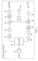
- Fig. 1 illustrates a block diagram of the front end of a wireless terminal that employs a dynamic power amplifier in accordance with one embodiment of the invention.
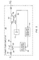
- Fig. 2 illustrates a block diagram of a dynamic power amplifier in accordance with one embodiment of the invention.
- Fig. 3a illustrates a block diagram of a power amplifier employed in a dynamic power amplifier in accordance with an embodiment of the invention.
- Fig. 3b illustrates a block diagram of a power amplifier employed in a dynamic power amplifier in accordance with another embodiment of the invention.
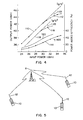
- Fig. 4 illustrates a plot of power response characteristics of a transistor employed in a dynamic power amplifier in accordance with an embodiment of the invention.
- Fig. 5 illustrates a communications system comprising a base station and a receiver employing a dynamic power amplifier in accordance with one embodiment of the invention.
- Fig. 1 illustrates a block diagram of the front end of a typical wireless terminal 10 employed in cellular communications system that incorporates a power amplifier 36 in accordance with one embodiment of the present invention, although the invention is not limited in scope in that respect.
- Fig. 5 illustrates a communications system comprising a base terminal 8 and a plurality of wireless terminals 10, which advantageously employ a power amplifier 36 in accordance with one embodiment of the invention.
- antenna 12 is configured to receive signals from a base station 8, and to transmit signals from the wireless terminal back to the base station.
- the output terminal of antenna 12 is coupled to an input terminal of a duplexer 14.
- Duplexer 14 is designed to route incoming signals from the base station to the upper signal path of wireless terminal 10, and to route signals from the lower path of the wireless terminal to antenna 12.
- Signals received by antenna 12 are routed through duplexer 14 to an input terminal of a bandpass filter 16, which is tuned to a desired frequency band intended for the wireless terminal.
- the output signal of bandpass filter 16 is amplified by low noise amplifier 18, which has an input terminal coupled to the output terminal of the bandpass filter.
- a mixer 20 receives the output signal of low noise amplifier 18 and a constant frequency signal from voltage-controlled oscillator 26.
- Mixer 20 down-converts the frequency of the signal received from low noise amplifier 18, and provides the down-converted signal to a bandpass filter 22.
- the output signal of bandpass filter 22 is then applied to an automatic gain control amplifier 24.
- the output signal of automatic gain control amplifier 24 is then provided to a signal processing circuit (not shown) for converting the received signal into speech and/or data.
- amplifier 28 receives and amplifies the signal intended to be transmitted to a base station.
- the output signal of amplifier 28 is then applied to a mixer 30, which also receives a constant frequency signal from voltage-controlled oscillator 26.
- Mixer 30 up-converts the signals received from amplifier 28 to a radio frequency RF signal.
- the output signal of mixer 30 is coupled to an input terminal of a bandpass filter 32.
- the output signal of bandpass 32 is provided to a driver 34, which generates a radio frequency RF signal having a given power signal level.
- the output signal of driver 34 is coupled to an input terminal of a dynamic power amplifier such as amplifier 36 in accordance with one embodiment of the present invention.
- a dynamic power amplifier such as amplifier 36 in accordance with one embodiment of the present invention.
- the output signal of dynamic power amplifier 36 is coupled to antenna 32 via duplexer 14.
- the input power signal level coupled to amplifier 36 depends on the distance of the wireless terminal from the base station. As the distance from the wireless terminal to the base station increases, the required input power signal coupled to amplifier 36 increases also. Conversely, as the distance from the wireless terminal to the base station decreases, the required input power signal coupled to amplifier 36 decreases also. However, with prior art power amplifiers, as the input power signal decreases the efficiency of the amplifier would substantially decrease also. As it will be explained in more detail hereinafter, in accordance with one aspect of the present invention, dynamic power amplifier 36 adjusts its biasing signals so that the amplifier operates at a substantially high efficiency region for a substantially wide range of input power signal levels.
- Fig. 2 illustrates a block diagram of a dynamic power amplifier, such as 36, in accordance with one embodiment of the present invention, although the invention is not limited in scope in that respect.
- the input terminal of dynamic power amplifier 36 receives a voltage signal from the output terminal of driver 34 (Fig. 1). This voltage signal is coupled to an input terminal of a power amplifier 38.
- power amplifier 38 comprise a bipolar junction transistor (BJT), or a field effect transistor (FET), although the invention is not limited in scope in that respect.
- BJT bipolar junction transistor
- FET field effect transistor
- the output voltage signal of power amplifier 38 is coupled to an input terminal of a power sensing device such as coupler 40.
- coupler 40 may be a directional coupler such as the one manufactured by Mini-Circuits TM , Brooklyn, New York.
- the basic function of a directional coupler is to receive an input signal and to provide two output signals that correspond to the input signal.
- the output signals are not equal in amplitude.
- the large power output signal is at the main-line output port 48, and, the smaller power indication signal is at the coupled port 50.
- directional coupler 40 it is possible to monitor and sense the power signal level at the output terminal of power amplifier 38 independent of load conditions at the output of dynamic power amplifier 36.
- envelope detector 44 is a capacitor-diode network that measures approximately the average value of the power indication signal provided by coupler 40.
- the output signal of envelope detector 44 is substantially a direct current (DC) average voltage signal, which corresponds to the output power level of power amplifier 38.
- DC direct current
- the output terminal of the envelope detector is coupled to an input terminal of a direct current (DC) offset converter 46.
- DC offset converter 46 generates a substantially direct current (DC) biasing voltage signal that corresponds to the magnitude of the average output voltage signal provided by envelope detector 44.
- the direct current (DC) biasing voltage signal of converter 46 is coupled to an input terminal 52 of power amplifier 38, as it will be explained in more detail hereinafter, with reference to Figs.3a and 3b.
- Fig. 3a illustrates a block diagram of a power amplifier 38 in accordance with one embodiment of the present invention, although the invention is not limited in scope in that respect.
- Voltage signal coupled to terminal 54 is in turn applied to an input terminal of an input matching network 60.
- input matching network 60 comprises a resistance, a capacitance and an inductance and provides impedance matching between the output stage of driver 34 (Fig. 1), and the input stage of amplifier 38.
- the output terminal of input matching network 60 is coupled to the base terminal of a transistor 64.
- Transistor 64 is preferably a power BJT transistor that is configured to operate at high frequencies.
- the base terminal of transistor 64 is also configured to receive a direct current voltage signal from a base bias network 62.
- Base bias network 62 receives a substantially direct current (DC) biasing voltage signal from converter 46 via terminal 52.
- Base bias network 62 is preferably a low pass filter that is configured to prevent high frequency signals from traveling to or from transistor 64 via the base bias network.
- the emitter terminal of transistor 64 is coupled to the ground signal level.
- the collector terminal of transistor 64 is coupled to a collector bias network 66.
- Collector bias network 66 receives a substantially constant direct current (DC) voltage signal from a constant DC voltage source, such as a battery, via terminal 67, and provides a biasing current to transistor 64.
- the collector bias network may be configured as a low pass filter to prevent high frequency signals from traveling to or from transistor 64 via the collector bias network.
- the collector terminal of transistor 64 is also coupled to an input terminal of an output matching network 68, which is configured to provide impedance-matching between the output stage of power amplifier 38 and input stage of duplexer 14 (Fig. 1).
- Fig. 3b illustrates a block diagram of power amplifier 38 employing a field effect transistor (FET) 74, instead of a bipolar junction transistor BJT 64 of Fig. 3a.
- FET field effect transistor
- BJT 64 bipolar junction transistor
- dynamic power amplifier 36 adjusts the biasing voltage signals of power amplifier 38 based on the power signal level at the output terminal of power amplifier 38.
- Coupler 40 monitors the power signal level and provides a corresponding power indication voltage signal at terminal 50.
- envelope detector 44 is preferably employed to provide an average voltage signal which corresponds to the average power signal level at the output of power amplifier 38.
- converter 46 Based on this average power signal level, converter 46 provides a corresponding biasing signal to terminal 52 of base bias network 62.
- the change in biasing signal changes the operating point of transistor 64 such that the transistor maintains a substantially linear characteristics.
- the converter provides a biasing voltage signal that allows transistor 64 to operate at a substantially high efficiency for a wide range of power signal levels.
- the efficiency of transistor 64 depends, among other things, on the input power signal level provided at its input terminal. For a transistor that is biased at a fixed biasing point, the efficiency of the transistor decreases as the input power signal level decreases.
- the collector voltage signal and the collector current remain constant regardless of variations in the input and output power signal levels. Thus, power added efficiency decreases as the power levels of input and output signals decrease.
- the collector voltage signal and the collector current signal vary as the output power signal detected by envelope detector 44 varies.
- offset DC converter 46 applies a lower voltage signal to base bias network 62.
- the collector current of transistor 64 also decreases and the power added efficiency of the transistor remains substantially constant.
- G 1dB G o (dB) - 1 where G o (dB) is the small-signal linear power gain in decibels.
- a typical plot 110 of P output versus P input which illustrates the 1-dB gain compression point 112 , is shown in Fig. 4.
- the power response characteristic of the transistor may be different depending on the value of base current signal, I B .
- Fig. 4 illustrates that for the same value of base current signal, the power added efficiency decreases as output power and input power signal levels decrease. However, it is possible to maintain the same power added efficiency by varying the value of the base signal current I B .
- converter 46 may be configured such that for a given output power signal, it applies a direct current voltage signal to base bias network 62 in accordance with power response characteristics illustrated in Fig. 4. To this end, it may be possible to maintain the power gain of the transistor at l-db gain compression point for a wide range of power output signals generated by amplifier 38.
- transistor 64 is equally applicable to a power amplifier that employs a field effect transistor (FET) 74.
- FET field effect transistor
- dynamic power amplifier 36 may be configured such that coupler 40 monitors the input power signal level instead of the output power signal level illustrated in Fig. 2.
- the detected input power signal level may be coupled to an input terminal of envelop detector 44, which in turn causes converter 46 to vary the biasing signals of the transistor employed in power amplifier 38.
- the present invention allows high frequency power amplifiers such as those employed in battery driven wireless terminals or other battery driven devices, to operate linearly at substantially high power added efficiency for a wide range of input and output power signal levels.
- high frequency power amplifiers such as those employed in battery driven wireless terminals or other battery driven devices
- this results in an extended battery life and more reliable device.
Landscapes
- Engineering & Computer Science (AREA)
- Power Engineering (AREA)
- Amplifiers (AREA)
- Control Of Amplification And Gain Control (AREA)
- Transceivers (AREA)
- Mobile Radio Communication Systems (AREA)
Applications Claiming Priority (2)
| Application Number | Priority Date | Filing Date | Title |
|---|---|---|---|
| US637999 | 1996-04-25 | ||
| US08/637,999 US5724005A (en) | 1996-04-25 | 1996-04-25 | Linear power amplifier with automatic gate/base bias control for optimum efficiency |
Publications (2)
| Publication Number | Publication Date |
|---|---|
| EP0803973A1 true EP0803973A1 (de) | 1997-10-29 |
| EP0803973B1 EP0803973B1 (de) | 2002-11-27 |
Family
ID=24558237
Family Applications (1)
| Application Number | Title | Priority Date | Filing Date |
|---|---|---|---|
| EP97302561A Expired - Lifetime EP0803973B1 (de) | 1996-04-25 | 1997-04-15 | Linearer Leistungsverstärker mit automatischer gate/base-Steuerung für optimalen Wirkungsgrad |
Country Status (4)
| Country | Link |
|---|---|
| US (1) | US5724005A (de) |
| EP (1) | EP0803973B1 (de) |
| JP (1) | JPH1041768A (de) |
| DE (1) | DE69717341T2 (de) |
Cited By (6)
| Publication number | Priority date | Publication date | Assignee | Title |
|---|---|---|---|---|
| GB2329087A (en) * | 1997-09-08 | 1999-03-10 | Motorola Inc | Improving the efficiency of a transmitter amplifier by controlling an amplifier voltage using a voltage conditioner such as a switched mode converter |
| GB2332997A (en) * | 1997-12-31 | 1999-07-07 | Samsung Electronics Co Ltd | Dynamic control to improve the efficiency of a variable power amplifier |
| WO2002065652A1 (de) * | 2001-02-09 | 2002-08-22 | Siemens Aktiengesellschaft | Verfahren zum energiesparenden betrieb eines mobilfunkgerätes und mobilfunkgerät |
| WO2002082638A1 (en) * | 2001-04-04 | 2002-10-17 | Qualcomm Incorporated | Bias adjustment for power amplifier |
| EP1293798B1 (de) * | 2001-08-21 | 2006-04-05 | EADS Deutschland GmbH | Sende/Empfangs-Modul einer aktiven phasengesteuerten Radarantenne |
| EP1512221A4 (de) * | 2002-06-11 | 2007-08-08 | Skyworks Solutions Inc | Leistungsverstärkungssystem mit versorgungs- und vorstromverbesserungen |
Families Citing this family (41)
| Publication number | Priority date | Publication date | Assignee | Title |
|---|---|---|---|---|
| JPH1155131A (ja) * | 1997-08-06 | 1999-02-26 | Nec Corp | 無線送信電力制御装置 |
| US6008698A (en) | 1998-05-18 | 1999-12-28 | Omnipoint Corporation | Amplifier with dynamically adaptable supply current |
| US6173163B1 (en) * | 1998-06-30 | 2001-01-09 | Ericsson Inc. | Switched sampling systems and methods for monitoring radio transmit power |
| US6418304B1 (en) * | 1998-09-16 | 2002-07-09 | Lucent Technologies Inc. | Method and apparatus for improving efficiency of high-power linear amplifier |
| US6396350B2 (en) | 2000-02-09 | 2002-05-28 | Paradigm Wireless Systems, Inc. | Power booster method and apparatus for improving the performance of radio frequency linear power amplifiers |
| US6625238B2 (en) * | 2000-03-29 | 2003-09-23 | Sony Corporation | Low power and high linearity receivers with reactively biased front ends |
| US6668028B1 (en) | 2000-03-29 | 2003-12-23 | Sony Corporation | Low-power CDMA receiver |
| US6825719B1 (en) | 2000-05-26 | 2004-11-30 | Intel Corporation | RF power amplifier and methods for improving the efficiency thereof |
| CA2380829A1 (en) * | 2000-05-31 | 2001-12-06 | Sony Corporation | Power detecting circuit and demodulator comprising the same |
| US6735424B1 (en) * | 2000-06-14 | 2004-05-11 | The Regents Of The University Of California | S-band low-noise amplifier with self-adjusting bias for improved power consumption and dynamic range in a mobile environment |
| US6342812B1 (en) | 2000-06-27 | 2002-01-29 | International Business Machines Corporation | Power amplification system for low power radio frequency signals |
| US6587511B2 (en) | 2001-01-26 | 2003-07-01 | Intel Corporation | Radio frequency transmitter and methods thereof |
| US6760604B2 (en) * | 2001-01-29 | 2004-07-06 | Motorola, Inc. | Portable radio transceiver having shared power source for audio and RF amplifiers |
| US6404284B1 (en) | 2001-04-19 | 2002-06-11 | Anadigics, Inc. | Amplifier bias adjustment circuit to maintain high-output third-order intermodulation distortion performance |
| US7061993B2 (en) * | 2001-08-29 | 2006-06-13 | Sony Corporation | CDMA receiver architecture for lower bypass switch point |
| US20030125065A1 (en) * | 2001-12-27 | 2003-07-03 | Ilan Barak | Method and apparatus for generating an output signal |
| US20030123566A1 (en) * | 2001-12-27 | 2003-07-03 | Jaime Hasson | Transmitter having a sigma-delta modulator with a non-uniform polar quantizer and methods thereof |
| US6687491B2 (en) * | 2002-01-18 | 2004-02-03 | Sony Corporation | Direct conversion of low power high linearity receiver |
| US7336753B2 (en) * | 2003-06-26 | 2008-02-26 | Marvell International Ltd. | Transmitter |
| US7912145B2 (en) * | 2003-12-15 | 2011-03-22 | Marvell World Trade Ltd. | Filter for a modulator and methods thereof |
| US7356315B2 (en) * | 2003-12-17 | 2008-04-08 | Intel Corporation | Outphasing modulators and methods of outphasing modulation |
| KR100592767B1 (ko) * | 2003-12-26 | 2006-06-26 | 한국전자통신연구원 | 개선된 전력증폭기 효율을 가진 듀얼 안테나 다이버시티송신기 및 시스템 |
| US7327803B2 (en) | 2004-10-22 | 2008-02-05 | Parkervision, Inc. | Systems and methods for vector power amplification |
| US7355470B2 (en) * | 2006-04-24 | 2008-04-08 | Parkervision, Inc. | Systems and methods of RF power transmission, modulation, and amplification, including embodiments for amplifier class transitioning |
| US8334722B2 (en) | 2007-06-28 | 2012-12-18 | Parkervision, Inc. | Systems and methods of RF power transmission, modulation and amplification |
| US9106316B2 (en) | 2005-10-24 | 2015-08-11 | Parkervision, Inc. | Systems and methods of RF power transmission, modulation, and amplification |
| US7911272B2 (en) | 2007-06-19 | 2011-03-22 | Parkervision, Inc. | Systems and methods of RF power transmission, modulation, and amplification, including blended control embodiments |
| US7937106B2 (en) | 2006-04-24 | 2011-05-03 | ParkerVision, Inc, | Systems and methods of RF power transmission, modulation, and amplification, including architectural embodiments of same |
| US8031804B2 (en) * | 2006-04-24 | 2011-10-04 | Parkervision, Inc. | Systems and methods of RF tower transmission, modulation, and amplification, including embodiments for compensating for waveform distortion |
| US7620129B2 (en) * | 2007-01-16 | 2009-11-17 | Parkervision, Inc. | RF power transmission, modulation, and amplification, including embodiments for generating vector modulation control signals |
| WO2008144017A1 (en) | 2007-05-18 | 2008-11-27 | Parkervision, Inc. | Systems and methods of rf power transmission, modulation, and amplification |
| WO2008156800A1 (en) | 2007-06-19 | 2008-12-24 | Parkervision, Inc. | Combiner-less multiple input single output (miso) amplification with blended control |
| US7768353B2 (en) * | 2008-06-13 | 2010-08-03 | Samsung Electro-Mechanics Company, Ltd. | Systems and methods for switching mode power amplifier control |
| KR20140026458A (ko) | 2011-04-08 | 2014-03-05 | 파커비전, 인크. | Rf 전력 송신, 변조 및 증폭 시스템들 및 방법들 |
| KR20140034895A (ko) | 2011-06-02 | 2014-03-20 | 파커비전, 인크. | 안테나 제어 |
| US9325535B2 (en) * | 2011-09-27 | 2016-04-26 | Skyworks Solutions, Inc. | Apparatus and methods for variable DC bias to improve linearity in signal processing circuits |
| CN106415435B (zh) | 2013-09-17 | 2020-08-11 | 帕克维辛股份有限公司 | 用于呈现信息承载时间函数的方法、装置和系统 |
| CN106663955B (zh) | 2014-08-04 | 2020-03-31 | 苹果公司 | 通过电源管脚在附件和对接底座之间进行通信 |
| KR102733482B1 (ko) | 2018-12-26 | 2024-11-25 | 삼성전자 주식회사 | 무선 통신 시스템에서 신호 레벨을 조정하는 장치 및 방법 |
| US11023007B2 (en) | 2019-04-02 | 2021-06-01 | Apple Inc. | Connection and moisture detection |
| KR102912017B1 (ko) * | 2024-12-30 | 2026-01-12 | 국립한밭대학교 산학협력단 | 전력 증폭기용 rc 필터 기반의 적응형 선형화 회로 장치 |
Citations (8)
| Publication number | Priority date | Publication date | Assignee | Title |
|---|---|---|---|---|
| JPS57152734A (en) * | 1981-03-18 | 1982-09-21 | Fujitsu Ltd | Control system for output power of radio transmitter |
| US4547746A (en) * | 1984-04-09 | 1985-10-15 | Rockwell International Corporation | VSWR Tolerant linear power amplifier |
| WO1990013173A1 (en) * | 1989-04-24 | 1990-11-01 | Telenokia Oy | High-frequency amplifier of a radio transmitter |
| EP0401013A2 (de) * | 1989-05-31 | 1990-12-05 | Nec Corporation | Hochfrequenzverstärker mit Optimierung des Stromverbrauches |
| WO1992005631A1 (en) * | 1990-09-25 | 1992-04-02 | Telenokia Oy | Method and arrangement for automatic gain control of a radio-frequency power amplifier |
| EP0488385A1 (de) * | 1990-11-30 | 1992-06-03 | Nec Corporation | FET-Verstärker mit Gate-Spannungsteuerung |
| WO1994001930A1 (en) * | 1992-07-02 | 1994-01-20 | Motorola Inc. | Rf amplifier bias control method and apparatus |
| EP0717504A2 (de) * | 1994-12-15 | 1996-06-19 | Nokia Mobile Phones Ltd. | Verfahren und Schaltung eines Funksenders |
Family Cites Families (5)
| Publication number | Priority date | Publication date | Assignee | Title |
|---|---|---|---|---|
| US4462004A (en) * | 1982-03-18 | 1984-07-24 | At&T Bell Laboratories | Dynamic class-4 FET amplifier |
| JP2609310B2 (ja) * | 1988-12-22 | 1997-05-14 | 株式会社日立製作所 | 送信回路 |
| JPH05267585A (ja) * | 1992-03-19 | 1993-10-15 | Mitsubishi Electric Corp | 増幅器 |
| JPH07154169A (ja) * | 1993-11-30 | 1995-06-16 | Matsushita Electric Ind Co Ltd | 高周波電力増幅器 |
| US5589796A (en) * | 1994-11-01 | 1996-12-31 | Motorola, Inc | Method and apparatus for increasing amplifier efficiency |
-
1996
- 1996-04-25 US US08/637,999 patent/US5724005A/en not_active Expired - Lifetime
-
1997
- 1997-04-15 EP EP97302561A patent/EP0803973B1/de not_active Expired - Lifetime
- 1997-04-15 DE DE69717341T patent/DE69717341T2/de not_active Expired - Lifetime
- 1997-04-21 JP JP9102886A patent/JPH1041768A/ja active Pending
Patent Citations (8)
| Publication number | Priority date | Publication date | Assignee | Title |
|---|---|---|---|---|
| JPS57152734A (en) * | 1981-03-18 | 1982-09-21 | Fujitsu Ltd | Control system for output power of radio transmitter |
| US4547746A (en) * | 1984-04-09 | 1985-10-15 | Rockwell International Corporation | VSWR Tolerant linear power amplifier |
| WO1990013173A1 (en) * | 1989-04-24 | 1990-11-01 | Telenokia Oy | High-frequency amplifier of a radio transmitter |
| EP0401013A2 (de) * | 1989-05-31 | 1990-12-05 | Nec Corporation | Hochfrequenzverstärker mit Optimierung des Stromverbrauches |
| WO1992005631A1 (en) * | 1990-09-25 | 1992-04-02 | Telenokia Oy | Method and arrangement for automatic gain control of a radio-frequency power amplifier |
| EP0488385A1 (de) * | 1990-11-30 | 1992-06-03 | Nec Corporation | FET-Verstärker mit Gate-Spannungsteuerung |
| WO1994001930A1 (en) * | 1992-07-02 | 1994-01-20 | Motorola Inc. | Rf amplifier bias control method and apparatus |
| EP0717504A2 (de) * | 1994-12-15 | 1996-06-19 | Nokia Mobile Phones Ltd. | Verfahren und Schaltung eines Funksenders |
Non-Patent Citations (2)
| Title |
|---|
| PATENT ABSTRACTS OF JAPAN vol. 006, no. 254 (E - 148) 14 December 1982 (1982-12-14) * |
| ROSENAUER D F: "DSP BASED TRANSMITTER GAIN CONTROL FOR SATELLITE EARTH STATIONS WITH MULTI-CARRIER BURST TRAFFIC", PROCEEDINGS OF THE PACIFIC RIM CONFERENCE ON COMMUNICATIONS, COMPUTERS AND SIGNAL PROCESSING, VICTORIA, JUNE 1 - 2, 1989, no. -, 1 June 1989 (1989-06-01), INSTITUTE OF ELECTRICAL AND ELECTRONICS ENGINEERS, pages 475 - 477, XP000077525 * |
Cited By (7)
| Publication number | Priority date | Publication date | Assignee | Title |
|---|---|---|---|---|
| GB2329087A (en) * | 1997-09-08 | 1999-03-10 | Motorola Inc | Improving the efficiency of a transmitter amplifier by controlling an amplifier voltage using a voltage conditioner such as a switched mode converter |
| GB2332997A (en) * | 1997-12-31 | 1999-07-07 | Samsung Electronics Co Ltd | Dynamic control to improve the efficiency of a variable power amplifier |
| GB2332997B (en) * | 1997-12-31 | 1999-11-24 | Samsung Electronics Co Ltd | Dynamic control of a variable power amplifier |
| WO2002065652A1 (de) * | 2001-02-09 | 2002-08-22 | Siemens Aktiengesellschaft | Verfahren zum energiesparenden betrieb eines mobilfunkgerätes und mobilfunkgerät |
| WO2002082638A1 (en) * | 2001-04-04 | 2002-10-17 | Qualcomm Incorporated | Bias adjustment for power amplifier |
| EP1293798B1 (de) * | 2001-08-21 | 2006-04-05 | EADS Deutschland GmbH | Sende/Empfangs-Modul einer aktiven phasengesteuerten Radarantenne |
| EP1512221A4 (de) * | 2002-06-11 | 2007-08-08 | Skyworks Solutions Inc | Leistungsverstärkungssystem mit versorgungs- und vorstromverbesserungen |
Also Published As
| Publication number | Publication date |
|---|---|
| US5724005A (en) | 1998-03-03 |
| DE69717341T2 (de) | 2003-07-03 |
| JPH1041768A (ja) | 1998-02-13 |
| DE69717341D1 (de) | 2003-01-09 |
| EP0803973B1 (de) | 2002-11-27 |
Similar Documents
| Publication | Publication Date | Title |
|---|---|---|
| US5724005A (en) | Linear power amplifier with automatic gate/base bias control for optimum efficiency | |
| KR100312367B1 (ko) | 이동체통신장치및방법 | |
| US6965837B2 (en) | Method and arrangement for detecting load mismatch, and a radio device utilizing the same | |
| US7595694B2 (en) | Electronics parts for high frequency power amplifier | |
| US20050032499A1 (en) | Radio frequency power detecting circuit and method therefor | |
| US6615028B1 (en) | System and method for selecting amplifiers in a communications device | |
| US6236266B1 (en) | Bias circuit and bias supply method for a multistage power amplifier | |
| US7190935B2 (en) | Amplifier power detection circuitry | |
| EP0673112A1 (de) | Leistungsverstärker und Verfahren dazu | |
| US20060066396A1 (en) | Circuit for power amplification | |
| US7199652B2 (en) | Amplifier; and transmitter and communication device incorporating the same | |
| US6433641B1 (en) | Power amplifier and communication device including power amplifier | |
| US20010034217A1 (en) | System and method for selectively interconnecting amplifiers in a communications device | |
| JPH09232992A (ja) | トランシーバのrfデュプレクサバイパス方法 | |
| EP1573906B1 (de) | Linearitätskonservierung eines leistungsverstärkers ohne isolator durch dynamische anpassung von verstärkung und phase | |
| EP0895350A1 (de) | Verstärkungsgeregelter Kleinleistungsverstärker mit grossem Dynamik-Bereich | |
| US7408404B2 (en) | Preserving linearity of an isolator-free power amplifier by dynamically switching active devices | |
| US6441689B1 (en) | Transistor amplifier providing improved linear and return loss performance characteristics | |
| JPH0946264A (ja) | 線形変調無線送受信装置及びその電力制御方法 | |
| WO2004054096A1 (en) | Preserving linearity of an isolator-free power amplifier by dynamically adjusting bias and supply of active devices | |
| JP2007166101A (ja) | 電力増幅器および無線機 | |
| EP1265354A1 (de) | Verstärkerschaltung | |
| US20020028664A1 (en) | Control method and circuit for using a heterojunction bipolar transistor power amplifier in a zero intermediate frequency architecture transmitter | |
| GB2362523A (en) | A transceiver with the bias of an amplifier in the receiver controlled by a baseband processor | |
| US6687490B2 (en) | Transmission apparatus and method for a mobile communication terminal |
Legal Events
| Date | Code | Title | Description |
|---|---|---|---|
| PUAI | Public reference made under article 153(3) epc to a published international application that has entered the european phase |
Free format text: ORIGINAL CODE: 0009012 |
|
| AK | Designated contracting states |
Kind code of ref document: A1 Designated state(s): DE FR GB |
|
| RIN1 | Information on inventor provided before grant (corrected) |
Inventor name: LIN, JENSHAN Inventor name: CHEN, YOUNG-KAI |
|
| 17P | Request for examination filed |
Effective date: 19980416 |
|
| 17Q | First examination report despatched |
Effective date: 20000329 |
|
| GRAG | Despatch of communication of intention to grant |
Free format text: ORIGINAL CODE: EPIDOS AGRA |
|
| GRAG | Despatch of communication of intention to grant |
Free format text: ORIGINAL CODE: EPIDOS AGRA |
|
| GRAH | Despatch of communication of intention to grant a patent |
Free format text: ORIGINAL CODE: EPIDOS IGRA |
|
| GRAH | Despatch of communication of intention to grant a patent |
Free format text: ORIGINAL CODE: EPIDOS IGRA |
|
| GRAA | (expected) grant |
Free format text: ORIGINAL CODE: 0009210 |
|
| AK | Designated contracting states |
Kind code of ref document: B1 Designated state(s): DE FR GB |
|
| REG | Reference to a national code |
Ref country code: GB Ref legal event code: FG4D |
|
| REF | Corresponds to: |
Ref document number: 69717341 Country of ref document: DE Date of ref document: 20030109 |
|
| ET | Fr: translation filed | ||
| PLBE | No opposition filed within time limit |
Free format text: ORIGINAL CODE: 0009261 |
|
| STAA | Information on the status of an ep patent application or granted ep patent |
Free format text: STATUS: NO OPPOSITION FILED WITHIN TIME LIMIT |
|
| 26N | No opposition filed |
Effective date: 20030828 |
|
| REG | Reference to a national code |
Ref country code: DE Ref legal event code: R082 Ref document number: 69717341 Country of ref document: DE Representative=s name: DILG HAEUSLER SCHINDELMANN PATENTANWALTSGESELL, DE |
|
| REG | Reference to a national code |
Ref country code: FR Ref legal event code: PLFP Year of fee payment: 19 |
|
| PGFP | Annual fee paid to national office [announced via postgrant information from national office to epo] |
Ref country code: FR Payment date: 20150319 Year of fee payment: 19 Ref country code: GB Payment date: 20150324 Year of fee payment: 19 |
|
| PGFP | Annual fee paid to national office [announced via postgrant information from national office to epo] |
Ref country code: DE Payment date: 20160321 Year of fee payment: 20 |
|
| GBPC | Gb: european patent ceased through non-payment of renewal fee |
Effective date: 20160415 |
|
| REG | Reference to a national code |
Ref country code: FR Ref legal event code: ST Effective date: 20161230 |
|
| PG25 | Lapsed in a contracting state [announced via postgrant information from national office to epo] |
Ref country code: FR Free format text: LAPSE BECAUSE OF NON-PAYMENT OF DUE FEES Effective date: 20160502 Ref country code: GB Free format text: LAPSE BECAUSE OF NON-PAYMENT OF DUE FEES Effective date: 20160415 |
|
| REG | Reference to a national code |
Ref country code: DE Ref legal event code: R071 Ref document number: 69717341 Country of ref document: DE |