EP0802483A1 - Halbleiterspeichergerät mit Zeilenredundanz - Google Patents
Halbleiterspeichergerät mit Zeilenredundanz Download PDFInfo
- Publication number
- EP0802483A1 EP0802483A1 EP96830217A EP96830217A EP0802483A1 EP 0802483 A1 EP0802483 A1 EP 0802483A1 EP 96830217 A EP96830217 A EP 96830217A EP 96830217 A EP96830217 A EP 96830217A EP 0802483 A1 EP0802483 A1 EP 0802483A1
- Authority
- EP
- European Patent Office
- Prior art keywords
- redundancy
- signal
- memory device
- row
- address
- Prior art date
- Legal status (The legal status is an assumption and is not a legal conclusion. Google has not performed a legal analysis and makes no representation as to the accuracy of the status listed.)
- Granted
Links
- 239000004065 semiconductor Substances 0.000 title claims abstract description 23
- 230000002950 deficient Effects 0.000 claims abstract description 72
- 239000011159 matrix material Substances 0.000 claims abstract description 28
- 230000004913 activation Effects 0.000 claims description 22
- 230000003213 activating effect Effects 0.000 claims description 10
- 239000000872 buffer Substances 0.000 claims description 10
- 230000009849 deactivation Effects 0.000 claims 1
- 238000010586 diagram Methods 0.000 description 18
- 102100022103 Histone-lysine N-methyltransferase 2A Human genes 0.000 description 9
- 101001045846 Homo sapiens Histone-lysine N-methyltransferase 2A Proteins 0.000 description 9
- 230000007704 transition Effects 0.000 description 6
- 102100021908 3-mercaptopyruvate sulfurtransferase Human genes 0.000 description 5
- 101000753843 Homo sapiens 3-mercaptopyruvate sulfurtransferase Proteins 0.000 description 5
- 101000640206 Tityus serrulatus Alpha-mammal toxin Ts2 Proteins 0.000 description 5
- 102100031048 Coiled-coil domain-containing protein 6 Human genes 0.000 description 4
- 101000777370 Homo sapiens Coiled-coil domain-containing protein 6 Proteins 0.000 description 4
- 238000001514 detection method Methods 0.000 description 3
- 101100255205 Caenorhabditis elegans rsa-2 gene Proteins 0.000 description 2
- 230000008901 benefit Effects 0.000 description 2
- 230000008859 change Effects 0.000 description 2
- 238000006467 substitution reaction Methods 0.000 description 2
- 230000000295 complement effect Effects 0.000 description 1
- 230000008878 coupling Effects 0.000 description 1
- 238000010168 coupling process Methods 0.000 description 1
- 238000005859 coupling reaction Methods 0.000 description 1
- 230000000694 effects Effects 0.000 description 1
- 230000006870 function Effects 0.000 description 1
- 230000003068 static effect Effects 0.000 description 1
- 230000001360 synchronised effect Effects 0.000 description 1
- 230000001960 triggered effect Effects 0.000 description 1
Images




Classifications
-
- G—PHYSICS
- G11—INFORMATION STORAGE
- G11C—STATIC STORES
- G11C29/00—Checking stores for correct operation ; Subsequent repair; Testing stores during standby or offline operation
- G11C29/70—Masking faults in memories by using spares or by reconfiguring
- G11C29/78—Masking faults in memories by using spares or by reconfiguring using programmable devices
- G11C29/84—Masking faults in memories by using spares or by reconfiguring using programmable devices with improved access time or stability
Definitions
- the present invention relates to a semiconductor memory device with row redundancy.
- redundancy memory elements are conventionally provided to functionally replace defective memory elements: for example, since semiconductor memory devices comprise a matrix of memory cells arranged in rows (word lines) and columns (bit lines), redundancy word lines and/or redundancy bit lines are provided to functionally replace defective word lines and/or defective bit lines, respectively.
- redundancy memory elements are provided, a redundancy circuit must be provided for storing the addresses of the defective memory elements (defective addresses), comparing the stored defective addresses with a current address supplied to the memory device, preventing the activation of the addressed defective memory element and activating in substitution a redundancy memory element.
- an internal timing signal to provide a time basis for the read operation: the access to the matrix memory element is triggered by a change in the address configuration supplied to the memory device; an internal timing signal (Address Transition Detection or ATD) is generated when such a change in the address configuration is detected, and the ATD signal provides the timing of the read operation: for example, the ATD signal is used to preset the sensing circuits.
- ATD Address Transition Detection
- redundancy memory elements follows a path which is parallel to that leading to the selection of the matrix memory elements, and the redundancy element selection path is asynchronous, i.e. not synchronized with the internal timing signal.
- the redundancy circuit recognizes that the current address is a defective address, it inhibits the activation of the defective memory element by disabling the address decoder and enables the selection of the redundancy memory element.
- a semiconductor memory device comprising:
- the row address decoder is forcedly enabled independently of the current address supplied to the memory device. In this way, if previously a redundancy row were selected and the new address correspond to a non-defective row, it is not necessary to wait for the activation of the row address decoder after the new address has been recognized as non-defective: the row address decoder is always activated at the beginning of each read cycle. If the new address is a defective address, the row address decoder will be deactivated only after the internal timing signal has been deactivated. The access time of the memory device is thus reduced.
- the internal timing signal can be for example the address transition detection (ATD) signal normally provided in memory devices.
- ATD address transition detection
- redundancy row driver circuits can be provided having a greater driving strenght than the matrix row driver circuits of the row address decoder; stronger driver circuits obviously occupy a larger chip area, but this is possible because being the number of redundancy row is generally small with respect to the number of matrix rows, a small number of such stronger driver circuits must be provided, and the impact on the overall chip area is limited.
- a row redundancy circuit according to the present invention is schematically shown.
- the row redundancy circuit is intended to be integrated in a semiconductor memory device to allow the functional substitution of redundancy word lines for defective word lines of a memory matrix.
- the row redundancy circuit comprises a plurality (four in the shown example) of programmable non-volatile memory registers RR1-RR4 (redundancy registers) for storing addresses of defective matrix word lines (defective addresses).
- each redundancy register is capable of storing two defective addresses; however, this is not to be intended as a limitation of the present invention: more generally, the invention finds application also in row redundancy circuits comprising redundancy registers each one capable of storing a single defective address.
- the eight redundancy selection signals RSA1-4 and RSB1-4 supply (bus RS in Fig. 1) a buffer circuit 1 comprising eight redundancy word line drivers D1-D8, each driver driving a respective redundancy word line RW1-RW8 of a matrix 2 of redundancy memory cells.
- the eight redundancy selection signals RSA1-4 and RSB1-4 also supply a redundancy detector circuit 3.
- the redundancy detector circuit 3 activates a disable signal DIS which disables a row address decoder circuit 4; the row address decoder circuit 4 is known per-se (and therefore not shown in detail) and is supplied by a bus of row address signals RA for decoding the current address supplied to the memory device and selecting a respective word line WL of a matrix 5 of memory cells.
- the disable signal DIS is activated, the selection of the matrix word lines WL is inhibited.
- Selection of a matrix word line, as well as of a redundancy word line, means that the potential of the word line is driven to the high logic level (e.g., 5V o 3V).
- the decoder circuit 4 comprises a plurality of drivers, each one associated to a respective word line WL.
- the redundancy detector circuit 3 is further supplied by two control signals NOM and NST generated by a redundancy control circuit 5.
- the redundancy control circuit 5 also supplies the buffer circuit 1 with two control signals RRS and FRC; the structure and operation of the redundancy control circuit 5 will be explained in detail later on.
- the redundancy control circuit 5 is also supplied with three control signals REN, FR and TST generated by a control logic 6 provided in a per-se known way in the memory device to control the activation of several operation modes of the memory device (e.g., read mode, program mode, test modes, etc.).
- the redundancy control circuit 5 is also supplied by a first timing signal ATD and a second timing signal ECY generated internally in the memory device to provide an internal timing for the memory device.
- the row redundancy circuit comprises a first address configuration detector circuit 8, supplied by the row address signals RA, capable of detecting if the current configuration of the row address signals corresponds to the configuration stored in non-programmed (virgin) redundancy registers RR1-RR4 (i.e., the configuration stored in redundancy registers which are not utilized because the number of defective word lines in the memory matrix is less than the number of redundancy word lines); circuit 8 supplies the redundancy control circuit 5 a disable signal ALL1.
- the row redundancy circuit also comprises a second address configuration detector circuit 9 supplied by a sub-set RA0-RA3 of the row address signals RA for detecting a particular configuration of said sub-set of row address signals RA0-RA3, and for accordingly activating a control signal AD15 supplied to the redundancy registers RR1-RR4.
- Circuits 8 and 9 are further supplied by a test signal TST1 generated by the control logic 6.
- Fig. 1 Also schematically shown in Fig. 1 is a group 30 of tri-state buffers TB1-TB8 controlled by a test signal TST2 generated by the control logic 6.
- Test signal TST2 is activated in a particular test mode to selectively connect the redundancy word lines RW1-RW8 to an internal bus IB comprising signals driving output terminals I/O of the memory device. This is useful during the in-factory testing of the memory device for detecting, directly at the output terminals of the memory device, which of the redundancy word lines are used to functionally replace defective word lines.
- Fig. 2 is a schematic diagram of one of the redundancy registers RR1-RR4.
- the redundancy register comprises three groups G1, G2' and G2'' of memory units; a first group G1 comprises seven memory units MU4-MU10, a second group G2' comprises four memory units MU0-MU3 and a third group G2'' comprises four memory units MU0-MU3.
- Each one of the memory units MU4-MU10 in the first group G1 is supplied by a respective row address signal RA4-RA10; each one of the memory units MU0-MU3 in the second group G2' is supplied by a respective row address signal RA0-RA3; each one of the memory units MU0-MU3 in the third group G2'' is supplied by a respective one of the row address signals RA0-RA3.
- signals RA0-RA3 represent the four least significant bits of the row address code, and signals RA4-RA10 represent the seven most significant bits of the row address code.
- Each memory unit comprises a programmable non-volatile memory element (such as, for example, a fuse or an EPROM memory cell) storing a respective bit of a defective address, and a circuitry suitable for comparing the defective address bit stored therein with the respective bit of the current row address code supplied to the memory device.
- Each memory unit has a respective output signal O0'-O3', O0''-O3'' and O4-O10 which is activated when the respective bit of the current row address code supplied to the memory device coincides with the defective address bit stored in the respective memory element.
- Output Signals O0'-O3' of the second group G2' of memory units are supplied to an AND gate 15 whose output supplies a first switch SW1.
- Output signals O0''-O3'' of the third group G2'' of memory units supply an AND gate 17 which is also supplied by the signal AD15 generated by circuit 9 in Fig. 1; the output of AND gate 17 supplies a second switch SW2.
- the output signals O4-O10 of the first group G1 of memory units supply a NAND gate 18 whose output signal 19 controls switches SW1 and SW2 to close when activated (low logic level).
- the redundancy register also comprises a programming control circuit 20 supplied by a program enable control signal PGEN, generated by the control logic 6, and by two respective column address signals CAm, CAn.
- Circuit 20 generates two programming signals PEA, PEB: signal PEA enables programming of the memory units of the first and second groups G1 and G2', signal PEB enables programming of the memory units of the third group G2''.
- the column address signal CAm when activated, enables programming of one particular redundancy register among the four available.
- Column address signal CAn allows to select which one of the two program enable signals PEA, PEB is to be activated.
- Fig. 3 is a diagram of the redundancy detector circuit 3.
- Each one of the eight redundancy selection signals RSA1-4, RSB1-4 supplies a gate electrode of a respective N-channel MOSFET M1-M8.
- All the MOSFETs M1-M8 are connected in parallel to each other between a drain electrode 10 of a P-channel MOSFET M9 and a drain electrode 11 of an N-channel MOSFET M10;
- M9 has a source electrode connected to a voltage supply VDD, M10 has a source electrode connected to the ground reference voltage;
- M9 and M10 are controlled by the control signal NST generated by the redundancy control circuit 5.
- a further N-channel MOSFET M11 controlled by the control signal NOM also generated by the control circuit 5, is connected in parallel to MOSFETs M1-M8.
- the drain electrode 10 of M9 is supplied to an input of an inverter I1 whose output forms the disable signal DIS for the row address decoder 4.
- Inverter I1 also controls a P-channel MOSFET M12 connected between VDD and the drain electrode 10 of M9.
- Fig. 4 is a diagram showing the first and second address configuration detector circuits 8 and 9 for the generation of signals ALL1 and AD15:
- signal ALL1 forms the output of a decoding circuit comprising three AND gates 21, 22 and 23 supplied with the row address signals RA0-RA3, RA4-RA7 and RA8-RA10, respectively, and a NAND gate 24 supplied with the outputs of AND gates 21, 22, 23 and with the test signal TST1 generated by the control logic 6.
- Signal AD15 forms the output of another decoding circuit comprising the AND gate 21 and a NAND gate 25 supplied with the output of AND gate 21 and with the test signal TST1.
- Test signal TST1 is normally deactivated (high logic level), but it is activated in a particular test mode to prevent activation of signals ALL1 and AD15 independently of the address configuration.
- Fig. 5 is a schematic diagram showing the circuits for the generation of the first and second timing signals ATD and ECY.
- Signals supplied to address input terminals A1, A2...An of the memory device supply a per-se known address buffer circuit 12 which generates the address signals of the bus ADD.
- the address signals ADD are supplied to an address transition detector circuit 13 which, upon transition of at least one of the address signals ADD, activates the first timing signal ATD; signal ATD goes low and remains at the low logic level for a prescribed time, then it goes high again.
- Signal ATD supplies a circuit 14 which generates the second timing signal ECY; signal ECY is normally at the high logic level, and goes low when the ATD signal goes low; signal ECY remains low until the read operation has been completed, then it goes high again.
- Circuits 13 and 14 can be for example monostable circuits.
- Fig. 10 is a timing diagram showing the relationship between signals ADD, ATD and ECY.
- Fig. 6 is a diagram of the redundancy control circuit 5 of Fig. 1.
- Control signals NOM and NST are generated as logic functions of the input control signals ATD, ECY and ALL1.
- Signal RRS is either equal to the signal ATD or it is forced to ground.
- Signal FRC is either equal to the logic complement of signal FR or it is forced to the voltage supply VDD.
- signal NST is the output of an AND gate 26 having a first input supplied by signal ATD and a second input supplied by the output of an OR gate 27 supplied by signals ALL1 and ECY.
- Signal ATD is allowed to supply AND gate 26 unless test signal TST is activated (high logic level): in the latter case, a switch SW3 coupling signal ATD to AND gate 26 is open, and an N-channel MOSFET M15 is activated to force the input of AND gate 26 to ground; also, the output of AND gate 26 is allowed to supply signal NST unless the redundancy enable signal REN is activated (low logic level): in the latter case, a switch SW4 is open and a P-channel MOSFET M16 is activated to force signal NST to VDD.
- Signal REN also controls the generation of signal NOM: in fact, when REN is activated, a switch SW5 is open and signal ECY cannot supply signal NOM; in this condition signal NOM is pulled to VDD by a P-channel MOSFET M17 activated by signal REN.
- Signal RRS is equal to signal ATD, unless a switch SW6 is open; switch SW6 is controlled by an output of a NAND gate 28 having a first input supplied by signal REN, a second input supplied by signal ALL1 and a third input supplied by an output of a NOR gate 29 supplied by signals ECY and FRC; when switch SW6 is open, signal RRS is forced to ground by an N-channel MOSFET M18.
- signal FRC is the output of a switch SW7 controlled by signal ATD: when ATD is activated (low), switch SW7 is open and signal FRC is forced to VDD by a P-channel MOSFET M19 also controlled by signal ATD.
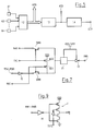
- Fig. 7 is a circuit diagram showing one of the redundancy word line drivers D1-D8 of the buffer circuit 1.
- Switch SW8 is controlled by signal RRS ad is open when RRS is low.
- switches SW8 and SW9 are open; the input of level shifter 31 is pulled to VDD by two P-channel MOSFETs M20, M21 connected in series between the input of level shifter 31 and VDD.
- final inverters I3 are realized to have a greater driving strength than the drivers in the row decoder circuit 4, so that the time needed to bring a redundancy word line to the high potential is less than the time needed to bring to the high potential a matrix word line.
- Fig. 8 shows the structure of the level shifter 31 of Fig. 7.
- the circuit comprises a cross-coupled structure having a first branch 310 and a second branch 311.
- the first branch 310 comprises a P-channel MOSFET and an N-channel MOSFET connected in series between the supply voltage VDD/VPP and ground.
- the second branch 311 comprises a P-channel MOSFET and an N-channel MOSFET connected in series between the supply voltage VDD/VPP and ground.
- the input of level shifter 31 forms a control signal for the N-channel MOSFET of the first branch and, after a logic inversion, for the N-channel MOSFET of the second branch.
- the gate electrodes of the P-channel MOSFETs in the first and second branch are respectively connected to the drain electrodes of the N-channel MOSFETs of the opposite branch.
- the output of the level shifter is connected to the drain electrode of the N-channel MOSFET in the second branch.
- Level shifter 31 is necessary because in program mode, when the voltage supply of the final inverter I3 is VPP (e.g., 12V), a high logic level of 5V or less at the input of final inverter I3 would cause a static current to flow in final inverter I3.
- Level shifter 31 raises the voltage at the input of inverter I3 to the VPP value.
- Level shifter 31, once set does not drain current from the voltage supply VDD/VPP.
- fig. 9 is a diagram showing one of the tri-state buffers TB1-TB8 of Fig. 1.
- the circuit comprises an inverter I4 supplied by a respective one of the eight redundancy word lines RW1-RW8.
- Inverter I4 controls a final tri-state inverter I5 which is activated by test signal TST2 and, when activated, drives a respective signal IBj of the internal bus IB of the memory device.
- the addresses of the matrix word lines containing defective memory cells are stored in the redundancy registers RR1-RR4.
- the control logic activates the signal PGEN; by means of the column address signals CAm, CAn it is possible to select which one of the four redundancy registers RR1-RR4 is to be programmed and, inside the selected redundancy register, the groups of memory units wherein the defective address is to be programmed.
- group G2' stores the four least significant bits RA0-RA3 of the defective address, while group G1 stores the seven most significant bits RA4-RA10 of the defective address.
- Group G2'' can be used to store a second defective address, provided that said second defective address shares with the already programmed defective address the seven most significant bits RA4-RA10. In this way, the number of memory units necessary to store two defective addresses is reduced, with a great benefit in terms of chip area.
- circuit 13 activates the normally-high signal ATD which goes low and remains low for a prescribed time (Fig. 10); signal ATD provides an internal timing signal for the memory device to perform the various phases of the read operation. Transition of signal ATD determines the activation of the normally-high signal ECY (Fig. 9), which goes low and remains low for a longer time than signal ATD; signal ECY returns to the high level when the read operation has been completed.
- row decoder circuit 4 decodes the current address and activates one of the word line drivers to select a word line WL of the matrix 50.
- Redundancy selection signals RSA1-4 and RSB1-4 are all deactivated. As long as signal ATD is low, signals NST and RRS are also low; in the redundancy detector circuit 3 M9 is on and M10 is off, and node 10 is pulled to VDD; signal DIS is deactivated, so that the row address decoder 4 is enabled. All the redundancy word line drivers D1-D8 are also deactivated (switch 8 is open, and the output of inverter I3 is low).
- Signal ECY also drives signal RRS low, so that the redundancy word line drivers D1-D8 are deactivated. In this way, at the end of the read cycle, both the matrix word line drivers in the row decoder 4 and the redundancy word line drivers D1-D8 are deactivated: this reduces the power consumption of the memory device and reduces the electric stress to which the memory cells and the redundancy memory cells are submitted.
- the current address supplied to the memory device is one of the defective addresses stored in the redundancy registers RR1-RR4.
- MOSFET M3 will be on; however, as long as signal ATD is low, signal NST is also low (Fig.
- the redundancy word line drivers D1-D8 are activated by signal RRS switching high: the redundancy selection signal RSA2 is supplied to the respective level shifter 31 and final inverter I3, carrying the potential of redundancy word line RW3 to VDD.
- signal ECY returns to the high level, causing switch SW6 in the redundancy control circuit 5 to open and determining the switching of signal RRS low: switch SW8 in the redundancy word line drivers D1-D8 opens and M21 turns on, so that all the redundancy word lines RW1-RW8 are deselected.
- bot the matrix word lines WL and the redundancy word lines RW1-RW8 are all deselected, to reduce power consumption and memory cells stress.
- the row decoder circuit 4 Since at the beginning of each read cycle the row decoder circuit 4 is always enabled even if in the previous read cycle a defective address has been supplied, it is not necessary to wait for the redundancy registers RR1-RR4 to recognize that the current address is not a defective address, and for the redundancy detector circuit 3 to deactivate the disable signal DIS. The access time of the memory device is thus improved.
- the delay in the selection path of the redundancy word lines RW1-RW8 caused by the fact that activation of the redundancy word line drivers D1-D8 is enabled only at the end of signal ATD can be easily compensated by making the final inverters I3 of the redundancy word line drivers to have a strong driving capability, i.e. by making their pull-up and pull-down transistors large in size; this has little effect in terms of chip area because the number of such final inverters is limited.
- circuit 9 activates signal AD15 which prevents the activation of all the redundancy selection signals RSB1-4: in this way, it is prevented that when such address configuration is supplied to the memory device the redundancy word lines associated to redundancy registers wherein the second group G2'' of memory units has never been programmed are simultaneously selected. Obviously, this means that when a defective address has the four least significant bits equal to "1"s, such address must be memorized in groups G1 and G2' of memory units of a selected redundancy memory register.
- Signal TST is activated by the control logic 6 in a particular test mode to prevent the row decoder 4 from being disabled even when the address supplied to the memory device is a defective address: when signal TST is activated (high logic level), switch SW3 (Fig. 6) opens and M15 turns on forcing the input of NAND 26 low; signal NST is thus forced low independently of the state of signal ATD; signal DIS is therefore forced low even if one of the redundancy selection signals RSA1-4, RSB1-4 is activated.
- Signal REN is activated by the control logic 6 in another particular test mode to forcedly disable row decoder 4: when signal REN is activated (low logic level), switches SW4 and SW5 in Fig. 6 are open, M16 and M17 are turned on, and signals NST and NOM are forced high; in the redundancy detector circuit 3 M9 is forced off, M10 on and M11 on, so that signal DIS is forced high, to deactivate the row decoder 4; also, activation of signal REN causes switch SW6 to open and M18 to turn on, forcing signal RRS low: all the redundancy word line drivers D1-D8 are thus deactivated.
- Signal FR is another test signal activated by the control logic in another test mode to allow the selection of the redundancy word lines to be directly controlled by respective row address signals: when signal FR is activated (low logic level), as long as signal ATD is low signal FRC is forced to ground, but when ATD returns to the high logic level signal FRC goes high and switches SW9 in the redundancy word line drivers D1-D8 close; the high level of signal FRC forces the output of NAND gate 28 in the redundancy control circuit 5 to the high level, thus opening switch SW6 and turning MOSFET M18 on: signal RRS is thus forced to ground.
- test signal FR can be activated in combination with signal REN.
- Signal TST2 is a further test signal activated by the control logic 6 in a further test mode: when signal TST2 is activated, tri-state buffers TB1-TB8 are activated, connecting the redundancy word lines RW1-RW8 to the internal bus IB of the memory device and thus driving directly output terminals I/O of the memory device.
- timing signal ATD could be any timing signal which is activated substantially at the beginning of a read cycle and which is deactivated after a prescribed time.
Landscapes
- For Increasing The Reliability Of Semiconductor Memories (AREA)
- Dram (AREA)
Priority Applications (3)
| Application Number | Priority Date | Filing Date | Title |
|---|---|---|---|
| DE69618928T DE69618928D1 (de) | 1996-04-18 | 1996-04-18 | Halbleiterspeichergerät mit Zeilenredundanz |
| EP96830217A EP0802483B1 (de) | 1996-04-18 | 1996-04-18 | Halbleiterspeichergerät mit Zeilenredundanz |
| US08/842,835 US5889710A (en) | 1996-04-18 | 1997-04-17 | Semiconductor memory device with row redundancy |
Applications Claiming Priority (1)
| Application Number | Priority Date | Filing Date | Title |
|---|---|---|---|
| EP96830217A EP0802483B1 (de) | 1996-04-18 | 1996-04-18 | Halbleiterspeichergerät mit Zeilenredundanz |
Publications (2)
| Publication Number | Publication Date |
|---|---|
| EP0802483A1 true EP0802483A1 (de) | 1997-10-22 |
| EP0802483B1 EP0802483B1 (de) | 2002-01-30 |
Family
ID=8225883
Family Applications (1)
| Application Number | Title | Priority Date | Filing Date |
|---|---|---|---|
| EP96830217A Expired - Lifetime EP0802483B1 (de) | 1996-04-18 | 1996-04-18 | Halbleiterspeichergerät mit Zeilenredundanz |
Country Status (3)
| Country | Link |
|---|---|
| US (1) | US5889710A (de) |
| EP (1) | EP0802483B1 (de) |
| DE (1) | DE69618928D1 (de) |
Families Citing this family (13)
| Publication number | Priority date | Publication date | Assignee | Title |
|---|---|---|---|---|
| JPH10302497A (ja) * | 1997-04-28 | 1998-11-13 | Fujitsu Ltd | 不良アドレスの代替方法、半導体記憶装置、及び、半導体装置 |
| US6052746A (en) * | 1998-04-14 | 2000-04-18 | Motorola, Inc. | Integrated circuit having programmable pull device configured to enable/disable first function in favor of second function according to predetermined scheme before/after reset |
| US6330635B1 (en) * | 1999-04-16 | 2001-12-11 | Intel Corporation | Multiple user interfaces for an integrated flash device |
| US6314030B1 (en) | 2000-06-14 | 2001-11-06 | Micron Technology, Inc. | Semiconductor memory having segmented row repair |
| US6728123B2 (en) | 2002-04-15 | 2004-04-27 | International Business Machines Corporation | Redundant array architecture for word replacement in CAM |
| EP1394810B1 (de) * | 2002-08-13 | 2007-10-10 | STMicroelectronics S.r.l. | Nichtflüchtige Speicheranordnung und Selbstreparatur-Verfahren |
| US7035152B1 (en) * | 2004-10-14 | 2006-04-25 | Micron Technology, Inc. | System and method for redundancy memory decoding |
| US7518196B2 (en) * | 2005-02-23 | 2009-04-14 | Intel Corporation | Field effect transistor with narrow bandgap source and drain regions and method of fabrication |
| JP4524636B2 (ja) * | 2005-03-24 | 2010-08-18 | エルピーダメモリ株式会社 | 半導体記憶装置 |
| US7858481B2 (en) * | 2005-06-15 | 2010-12-28 | Intel Corporation | Method for fabricating transistor with thinned channel |
| US20070090416A1 (en) * | 2005-09-28 | 2007-04-26 | Doyle Brian S | CMOS devices with a single work function gate electrode and method of fabrication |
| US7479421B2 (en) * | 2005-09-28 | 2009-01-20 | Intel Corporation | Process for integrating planar and non-planar CMOS transistors on a bulk substrate and article made thereby |
| KR102117633B1 (ko) * | 2013-09-12 | 2020-06-02 | 에스케이하이닉스 주식회사 | 셀프 리페어 장치 |
Citations (2)
| Publication number | Priority date | Publication date | Assignee | Title |
|---|---|---|---|---|
| US4811298A (en) * | 1986-08-22 | 1989-03-07 | International Business Machines Corporation | Decoding circuit arrangement for redundant semiconductor storage systems |
| EP0668563A1 (de) * | 1994-02-17 | 1995-08-23 | STMicroelectronics S.r.l. | Verfahren zur Programmierung von Redundanzregistern in einer Zeilenredundanzschaltung für einen Halbleiterspeicherbaustein |
Family Cites Families (2)
| Publication number | Priority date | Publication date | Assignee | Title |
|---|---|---|---|---|
| JP2577724B2 (ja) * | 1986-07-31 | 1997-02-05 | 三菱電機株式会社 | 半導体記憶装置 |
| JPS6433800A (en) * | 1987-07-29 | 1989-02-03 | Toshiba Corp | Semiconductor memory |
-
1996
- 1996-04-18 EP EP96830217A patent/EP0802483B1/de not_active Expired - Lifetime
- 1996-04-18 DE DE69618928T patent/DE69618928D1/de not_active Expired - Lifetime
-
1997
- 1997-04-17 US US08/842,835 patent/US5889710A/en not_active Expired - Lifetime
Patent Citations (2)
| Publication number | Priority date | Publication date | Assignee | Title |
|---|---|---|---|---|
| US4811298A (en) * | 1986-08-22 | 1989-03-07 | International Business Machines Corporation | Decoding circuit arrangement for redundant semiconductor storage systems |
| EP0668563A1 (de) * | 1994-02-17 | 1995-08-23 | STMicroelectronics S.r.l. | Verfahren zur Programmierung von Redundanzregistern in einer Zeilenredundanzschaltung für einen Halbleiterspeicherbaustein |
Also Published As
| Publication number | Publication date |
|---|---|
| DE69618928D1 (de) | 2002-03-14 |
| US5889710A (en) | 1999-03-30 |
| EP0802483B1 (de) | 2002-01-30 |
Similar Documents
| Publication | Publication Date | Title |
|---|---|---|
| US6081441A (en) | Content-addressable memory | |
| US5548225A (en) | Block specific spare circuit | |
| EP0809186B1 (de) | Verfahren und Gerät für Redundanz von nichtflüchtigen integrierten Speichern | |
| KR950005579B1 (ko) | 반도체 기억 장치 | |
| US5287310A (en) | Memory with I/O mappable redundant columns | |
| EP0802483B1 (de) | Halbleiterspeichergerät mit Zeilenredundanz | |
| EP0668563B1 (de) | Verfahren zur Programmierung von Redundanzregistern in einer Zeilenredundanzschaltung für einen Halbleiterspeicherbaustein | |
| JPH08339699A (ja) | 行デコーダおよびdram | |
| US4791615A (en) | Memory with redundancy and predecoded signals | |
| US6542419B2 (en) | Semiconductor integrated circuit device with electrically programmable fuse | |
| EP0622803B1 (de) | Adressenpuffer | |
| JPH08339696A (ja) | Ramアレイをテストする方法 | |
| US6498756B2 (en) | Semiconductor memory device having row repair circuitry | |
| JP2540028B2 (ja) | 集積プログラミング回路 | |
| US6058052A (en) | Redundancy scheme providing improvements in redundant circuit access time and integrated circuit layout area | |
| KR100342642B1 (ko) | 용장 회로를 구비한 반도체 기억 장치 | |
| US6310803B1 (en) | Semiconductor having mechanism capable of operating at high speed | |
| EP0802482B1 (de) | Redundanzspeicherregister | |
| US6061286A (en) | Memory device with reduced power dissipation | |
| JP3644868B2 (ja) | 活性化された多数本のワード線が順次ディスエーブルされる半導体メモリ装置 | |
| EP0811919B1 (de) | Speichergerät mit getakteter Spaltenredundanz | |
| US5796271A (en) | Memory array having redundant word line | |
| JPH09320296A (ja) | 半導体記憶装置 | |
| EP0811917B1 (de) | Schaltung um redundante Daten einer Redundanzschaltung innerhalb einer Speicheranordnung durch zeitgeteilte Annäherung zu übertragen | |
| EP0811918B1 (de) | Halbleiterspeicheranordnung mit getakteter Spalttenredundanz und zeitgeteilter redundanter Datenübertragung |
Legal Events
| Date | Code | Title | Description |
|---|---|---|---|
| PUAI | Public reference made under article 153(3) epc to a published international application that has entered the european phase |
Free format text: ORIGINAL CODE: 0009012 |
|
| AK | Designated contracting states |
Kind code of ref document: A1 Designated state(s): DE FR GB IT |
|
| 17P | Request for examination filed |
Effective date: 19980411 |
|
| RAP3 | Party data changed (applicant data changed or rights of an application transferred) |
Owner name: STMICROELECTRONICS S.R.L. |
|
| 17Q | First examination report despatched |
Effective date: 20001107 |
|
| GRAG | Despatch of communication of intention to grant |
Free format text: ORIGINAL CODE: EPIDOS AGRA |
|
| GRAG | Despatch of communication of intention to grant |
Free format text: ORIGINAL CODE: EPIDOS AGRA |
|
| GRAH | Despatch of communication of intention to grant a patent |
Free format text: ORIGINAL CODE: EPIDOS IGRA |
|
| GRAH | Despatch of communication of intention to grant a patent |
Free format text: ORIGINAL CODE: EPIDOS IGRA |
|
| GRAA | (expected) grant |
Free format text: ORIGINAL CODE: 0009210 |
|
| REG | Reference to a national code |
Ref country code: GB Ref legal event code: IF02 |
|
| AK | Designated contracting states |
Kind code of ref document: B1 Designated state(s): DE FR GB IT |
|
| PG25 | Lapsed in a contracting state [announced via postgrant information from national office to epo] |
Ref country code: FR Free format text: LAPSE BECAUSE OF FAILURE TO SUBMIT A TRANSLATION OF THE DESCRIPTION OR TO PAY THE FEE WITHIN THE PRESCRIBED TIME-LIMIT Effective date: 20020130 |
|
| REF | Corresponds to: |
Ref document number: 69618928 Country of ref document: DE Date of ref document: 20020314 |
|
| PG25 | Lapsed in a contracting state [announced via postgrant information from national office to epo] |
Ref country code: DE Free format text: LAPSE BECAUSE OF FAILURE TO SUBMIT A TRANSLATION OF THE DESCRIPTION OR TO PAY THE FEE WITHIN THE PRESCRIBED TIME-LIMIT Effective date: 20020501 |
|
| EN | Fr: translation not filed | ||
| PLBE | No opposition filed within time limit |
Free format text: ORIGINAL CODE: 0009261 |
|
| STAA | Information on the status of an ep patent application or granted ep patent |
Free format text: STATUS: NO OPPOSITION FILED WITHIN TIME LIMIT |
|
| 26N | No opposition filed | ||
| PGFP | Annual fee paid to national office [announced via postgrant information from national office to epo] |
Ref country code: GB Payment date: 20080326 Year of fee payment: 13 |
|
| PGFP | Annual fee paid to national office [announced via postgrant information from national office to epo] |
Ref country code: IT Payment date: 20080409 Year of fee payment: 13 |
|
| GBPC | Gb: european patent ceased through non-payment of renewal fee |
Effective date: 20090418 |
|
| PG25 | Lapsed in a contracting state [announced via postgrant information from national office to epo] |
Ref country code: GB Free format text: LAPSE BECAUSE OF NON-PAYMENT OF DUE FEES Effective date: 20090418 |
|
| PG25 | Lapsed in a contracting state [announced via postgrant information from national office to epo] |
Ref country code: IT Free format text: LAPSE BECAUSE OF NON-PAYMENT OF DUE FEES Effective date: 20090418 |