EP0802420A2 - Impedance measuring apparatus - Google Patents
Impedance measuring apparatus Download PDFInfo
- Publication number
- EP0802420A2 EP0802420A2 EP97302511A EP97302511A EP0802420A2 EP 0802420 A2 EP0802420 A2 EP 0802420A2 EP 97302511 A EP97302511 A EP 97302511A EP 97302511 A EP97302511 A EP 97302511A EP 0802420 A2 EP0802420 A2 EP 0802420A2
- Authority
- EP
- European Patent Office
- Prior art keywords
- impedance
- measuring apparatus
- measurement
- measurement range
- impedance measuring
- Prior art date
- Legal status (The legal status is an assumption and is not a legal conclusion. Google has not performed a legal analysis and makes no representation as to the accuracy of the status listed.)
- Granted
Links
Images


Classifications
-
- G—PHYSICS
- G01—MEASURING; TESTING
- G01R—MEASURING ELECTRIC VARIABLES; MEASURING MAGNETIC VARIABLES
- G01R27/00—Arrangements for measuring resistance, reactance, impedance, or electric characteristics derived therefrom
- G01R27/02—Measuring real or complex resistance, reactance, impedance, or other two-pole characteristics derived therefrom, e.g. time constant
-
- G—PHYSICS
- G01—MEASURING; TESTING
- G01R—MEASURING ELECTRIC VARIABLES; MEASURING MAGNETIC VARIABLES
- G01R35/00—Testing or calibrating of apparatus covered by the other groups of this subclass
- G01R35/005—Calibrating; Standards or reference devices, e.g. voltage or resistance standards, "golden" references
Definitions
- the present invention relates to an impedance measuring apparatus.
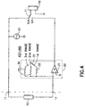
- FIG. 4 is a block diagram indicating the principle lying behind a typical prior art impedance measuring apparatus.
- the impedance measuring apparatus is provided with test signal source 51, current to voltage converter part 30, analog to digital (A-D) converter part 70, switch 71 and an arithmetic and control part (not shown in figure) for control thereof.
- test signal source 51 current to voltage converter part 30, analog to digital (A-D) converter part 70, switch 71 and an arithmetic and control part (not shown in figure) for control thereof.
- A-D analog to digital
- Test signal is applied from test signal source 51 to one terminal on a device under test (DUT) 10 via measurement terminal 11. Another terminal on DUT 10 is connected to current to voltage converter 30 via measurement terminal 12.
- Current to voltage converter part 30 is provided with an amplifier 31, a switch 35 and range resistors 32, 33 and 34. Range resistors 32, 33 or 34 are selected by switch 35 and are connected between the input and output terminals on amplifier 31.
- the input of current to voltage converter part 30 becomes equivalent to the ground potential by means of a feedback circuit which is made up of amplifier 31 and the resistors.
- the output becomes a voltage which is proportional to the input current.
- test signal source 51 that is, the voltage from measurement terminal 11 becomes equivalent to the voltage between both terminals on DUT 10.
- A-D converter 70 measures the voltage of the DUT.
- the output voltage from current to voltage converter part 30 is a voltage which is proportional to the current flowing through DUT 10.
- switch 71 is connected to the Ich side and is used to select the output voltage from current to voltage converter part 30, A-D converter 70 measures the current flowing through DUT 10.
- test voltage is constant, the current is proportional to the admittance of the DUT and the full scale of the measurement range is determined by the admittance.
- measured admittance value Y dut of the DUT is the product of the conductance Gi of the range resistors (32, 33 or 34) and the ratio I/V of I obtained by connecting switch 71 to the Ich terminal and the value V obtained by connecting switch 71 to the Vch terminal and carrying out A-D conversion.
- Y dut Gi • I / V
- i indicates the name of the range. This is calculated using the arithmetic and control unit.
- range resistors 32, 33 and 34 are switched using switch 35 and the current is converted and normalized to a voltage having a magnitude which can be measured with a high degree of accuracy by using the A-D converter 70.
- A-D converter 70 A-D converter
- calibration is carried out by multiple standards (working standards).
- the value of the respective standards (working standards) is selected so that they provide a full scale for the A-D converter 70 in the corresponding range. This means that the selection is made so that the optimum measured SN ratio can be obtained in each of the ranges.
- the corrected measured value is obtained by using the operation in the following formula using the correction coefficient Ki obtained by using this calibration.
- Y dut Ki • Gi • I / V
- An impedance measuring apparatus requires multiple calibration standards in order to calibrate multiple measurement ranges and a long time is required for this calibration process.
- An object of the present invention is to provide an impedance measuring apparatus capable of simply and rapidly carrying out a calibration of multiple impedance measurement ranges by using a single impedance standard.
- the impedance measuring apparatus is provided with a group of reference impedances.
- the relative error between the measurement ranges is automatically corrected internally using the reference impedances.
- the aforementioned basic means corrects the relative error among the measurement ranges by the mediation of the reference impedance. As a result, a measurement at a value which is smaller than the full scale of the range is inevitable. As a result, errors resulting from the resolution, linearity and the SN ratio are propagated throughout the ranges and accumulate. In order to prevent this, a signal normalizing part is placed in front of the A-D converter and frequency converter where such errors arise, thus avoiding measurement at a value which is smaller than the full scale.
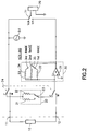
- Fig. 1 indicates a third practical embodiment of the present invention.
- Fig. 2 indicates a first practical embodiment of the present invention.
- Fig. 3 indicates a second practical embodiment of the present invention.
- Fig. 4 indicates an example of the prior art.
- Figure 2 indicates the configuration of the above-mentioned basic means which is used as the first practical embodiment of the present invention.
- the reference numerals are the same as for the configuration elements of the prior art apparatus indicated in Figure 4.
- the first practical embodiment provided here is an example which uses a resistor as the reference impedance for measuring the relative error among the ranges. Unlike the prior art indicated in Figure 4, there are added reference resistor part 20 and switch 24 which is switched between reference resistor part 20 and DUT 10. In addition, there is no need to calibrate resistors 21 and 22 in reference resistor part 20. Nor is there any need for long-term stability.
- the method for calibrating the absolute error of all of the ranges by measuring the relative error among the ranges is as follows. It is carried out by controlling from the arithmetic and control unit (not shown in the figure).
- calibration can be carried out even in a sequence opposite that used for calibrating the ranges mentioned previously. This means first evaluating the reference resistor at full scale and then calibrating 10 % of the range using the reference resistor. A sequence whereby calibration is carried out first using the standard resistor may also be adopted.
- measurement at 10 % of full scale (hereinafter referred to in abbreviated form as "10 % measurement”) is such that the measuring accuracy declines compared to when full scale is used.
- 10 % measurement is such that the measuring accuracy declines compared to when full scale is used.
- the primary cause of the errors is the deterioration of the signal to noise (SN) ratio, the resolution and the linearity when 10 % measurement is carried out.
- SN signal to noise
- the noise encountered is made up of thermal noise and "shot" noise of each of the elements making up the circuit and occurs in superimposed fashion on the signals.
- the SN ratio is 1/10 that of full scale.
- Gaussian noise a measurement time which is ten times that of full scale is required to obtain a measurement reproducibility (measurement error standard deviation) equal to that at full scale.
- the quantizing step size of the A-D converter as well as its un-uniformity adversely affect the measuring resolution and linearity.
- the 10 % measurement following a simple model, the error resulting from these multiplies tenfold.
- Figure 3 indicates a second practical embodiment of the means used to resolve the problems encountered in the first practical embodiment of the present invention.
- the sequence for calibrating reference resistor part 20 and the errors among the ranges is the same as for the first practical embodiment.
- Signal normalizer 60 is provided with transformer 61, amplifier 62 and switch 63.
- transformer 61 is provided with an output terminal and reduces the input voltage to 1/10 and the gain of amplifier 62 is set at 10.
- switch 63 is used to select x 10
- the gain of signal normalizer 60 is increased tenfold.
- switch 63 is used to select x 1
- the gain of signal normalizer 60 is unity.
- the gain of signal normalizer 60 need not be calibrated as long as a transformer is used.
- transformer 61 on signal normalizer 60 may be replaced with resistive divider depending on the measuring precision or the measuring frequency of the impedance measuring apparatus.
- Figure 1 indicates an example of a wide frequency band impedance measuring apparatus whose measuring frequency is 100 Hz to 100 MHz.
- the measuring frequency is mixed with local signals 53 and converted to an intermediate frequency at frequency converter 52. Then, it is measured using an A-D converter 70.
- Signal normalizing part 60 is provided at the intermediate frequency stage at the input to A-D converter 70 in order to eliminate any accumulation of errors resulting from deterioration of the resolution and linearity of A-D converter 70.
- the signal normalizer 60 operates in the same way as signal normalizing part 60 in the second practical embodiment of the present invention.
- the problem involving the SN ratio cannot be resolved solely by attaching signal normalizer 60 to the input of A-D converter 70 mentioned above.
- the SN ratio is usually limited by the dynamic range of frequency converter 52.
- the SN ratio becomes 1/10 of that which occurs when a full scale measurement is carried out. 100 times the measurement time as for a full scale measuring action is required to obtain the same standard deviation for measurement error as for full scale measurement.
- signal normalizing part 40 indicated in Figure 1 indicates such a configuration.
- signal normalizing part 40 is provided with a voltage divider made up of resistors 43 and 42, a switch 44 and an amplifier 41. If the gain for 10 % measurement is set at tenfold, as was the case for signal normalizing part 60, the noise problem caused by frequency converter 52 can be resolved.
- the voltage division ratio for signal normalizing part 40 is to be calibrated in the same way as the impedance range.
- signal normalizing part 40 is switched to x 10 and x 1 with a setting (10 % measurement) for measuring 1 mS reference resistor at a 10 mS range, and if signal normalizing part 60 on the intermediate frequency stage is switched in line with this to x 1 and x 10 and measurement is carried out, there is no deterioration in A-D conversion and the accurate gain ratio can be found for signal normalizing part 40.
- N - 1 times is required for 10 % measurement.
- 10 % measurement required for calibrating signal normalizing part 40 need be carried out only one time so that the calibration time can be shortened.
- the second effect comes about from the requirements for correcting the frequency characteristics for the wide frequency band impedance measuring apparatus.
- the values of these cover a wide range, there are great differences in the frequency characteristics in the various ranges due to parasitic capacity and the switching circuit. For that reason, a great number of calibration frequency points are required even assuming that interpolation has been carried out inside the frequency.
- signal normalizing part 40 can be configured with a simple circuit thus resulting in flat frequency characteristics.
- the calibration frequency points required to interpolate and correct all of the frequency bands of signal normalizing part 40 may be approximately 1/10 of that relative to the range.
- an impedance measuring apparatus which is so configured that a wide impedance range is covered by multiple ranges can be calibrated simply and rapidly using a single impedance standard.
- the present invention is further effective for wide band impedance measuring apparatuses and the type of calibration standard is not limited to either resistor or capacitor.
- the apparatus may also be used practically and effectively compared with conventional one that needs multiple standards, because present apparatus needs only one standard, and improves traceability and consistency among ranges.
Abstract
Description
- The present invention relates to an impedance measuring apparatus.
- Figure 4 is a block diagram indicating the principle lying behind a typical prior art impedance measuring apparatus. The impedance measuring apparatus is provided with
test signal source 51, current tovoltage converter part 30, analog to digital (A-D)converter part 70,switch 71 and an arithmetic and control part (not shown in figure) for control thereof. - The basic principle underlying the measuring process is as follows. Test signal is applied from
test signal source 51 to one terminal on a device under test (DUT) 10 viameasurement terminal 11. Another terminal onDUT 10 is connected to current tovoltage converter 30 viameasurement terminal 12. Current tovoltage converter part 30 is provided with anamplifier 31, aswitch 35 andrange resistors Range resistors switch 35 and are connected between the input and output terminals onamplifier 31. As a result, the input of current tovoltage converter part 30 becomes equivalent to the ground potential by means of a feedback circuit which is made up ofamplifier 31 and the resistors. In addition, the output becomes a voltage which is proportional to the input current. - The input of current to
voltage converter part 30, that is,measurement terminal 12, becomes ground potential. As a result, the output fromtest signal source 51, that is, the voltage frommeasurement terminal 11, becomes equivalent to the voltage between both terminals onDUT 10. - As a result, when
switch 71 is connected as indicated in Figure 4 to Vch and the test signal source is selected,A-D converter 70 measures the voltage of the DUT. Meanwhile, the output voltage from current tovoltage converter part 30 is a voltage which is proportional to the current flowing throughDUT 10. As a result, whenswitch 71 is connected to the Ich side and is used to select the output voltage from current tovoltage converter part 30,A-D converter 70 measures the current flowing throughDUT 10. - In the configuration indicated in Figure 4, the test voltage is constant, the current is proportional to the admittance of the DUT and the full scale of the measurement range is determined by the admittance. As a result, it is more appropriate to specify the measurement range using "admittance" rather than using "impedance".
- As indicated previously, measured admittance value Y dut of the DUT is the product of the conductance Gi of the range resistors (32, 33 or 34) and the ratio I/V of I obtained by connecting
switch 71 to the Ich terminal and the value V obtained by connectingswitch 71 to the Vch terminal and carrying out A-D conversion. In other words:
- Here, i indicates the name of the range. This is calculated using the arithmetic and control unit.
- Since the current flowing through the DUT greatly changes due to the impedance value (admittance value) of the DUT,
range resistors switch 35 and the current is converted and normalized to a voltage having a magnitude which can be measured with a high degree of accuracy by using theA-D converter 70. Although there are three measurement ranges in Figure 4, it should by no means be construed that the number of measurement ranges is limited to three. - In the impedance measuring apparatus including multiple measurement ranges switched, calibration is carried out by multiple standards (working standards). The value of the respective standards (working standards) is selected so that they provide a full scale for the
A-D converter 70 in the corresponding range. This means that the selection is made so that the optimum measured SN ratio can be obtained in each of the ranges. The corrected measured value is obtained by using the operation in the following formula using the correction coefficient Ki obtained by using this calibration.
- The conventional method of carrying out calibration for each measurement range which provided as many standards as there were ranges involved a large number of standards. The costs and management associated with such a method as well as the number of steps involved in the calibration process were burdensome both for the manufacturer and for the user.
- Therefore, an apparatus or a function which could be calibrated by using a single standard was ideal both for the manufacturer and the user. However, when the prior art impedance measuring apparatus was calibrated using a single standard, calibration could be carried out suitably only within a certain range. There was, however, a need for calibration in other ranges, under conditions which did not fulfill even 1 % of the full scale. Needless to say, this type of calibration method could not be applied to an impedance measuring apparatus which covered a wide measurement range.
- An impedance measuring apparatus requires multiple calibration standards in order to calibrate multiple measurement ranges and a long time is required for this calibration process.
- An object of the present invention is to provide an impedance measuring apparatus capable of simply and rapidly carrying out a calibration of multiple impedance measurement ranges by using a single impedance standard.
- In the basic means of the present invention, the impedance measuring apparatus is provided with a group of reference impedances. The relative error between the measurement ranges is automatically corrected internally using the reference impedances. By calibrating a single range using a single impedance standard, absolute calibration of all of the ranges can be carried out.
- The aforementioned basic means corrects the relative error among the measurement ranges by the mediation of the reference impedance. As a result, a measurement at a value which is smaller than the full scale of the range is inevitable. As a result, errors resulting from the resolution, linearity and the SN ratio are propagated throughout the ranges and accumulate. In order to prevent this, a signal normalizing part is placed in front of the A-D converter and frequency converter where such errors arise, thus avoiding measurement at a value which is smaller than the full scale.
- Fig. 1 indicates a third practical embodiment of the present invention.
- Fig. 2 indicates a first practical embodiment of the present invention.
- Fig. 3 indicates a second practical embodiment of the present invention.
- Fig. 4 indicates an example of the prior art.
-
- 10 :
- Device under test
- 11 :
- Measurement terminal
- 12 :
- Measurement terminal
- 20 :
- Reference resistor part
- 21 :
- Resistor
- 22 :
- Resistor
- 23 :
- Switch
- 24 :
- Switch
- 30 :
- Current to voltage converter
- 31 :
- Amplifier
- 32 :
- First range resistor
- 33 :
- Second range resistor
- 34 :
- Third range resistor
- 35 :
- Switch
- 40 :
- Signal normalizing part
- 41 :
- Amplifier
- 42 :
- Resistor
- 43 :
- Resistor
- 44 :
- Switch
- 51 :
- Test signal source
- 52 :
- Frequency converter
- 53 :
- Local signal
- 60 :
- Signal normalizing part
- 61 :
- Transformer
- 62 :
- Amplifier
- 63 :
- Switch
- 70 :
- A-D converter
- 71 :
- Switch
- Figure 2 indicates the configuration of the above-mentioned basic means which is used as the first practical embodiment of the present invention. The reference numerals are the same as for the configuration elements of the prior art apparatus indicated in Figure 4.
- The first practical embodiment provided here is an example which uses a resistor as the reference impedance for measuring the relative error among the ranges. Unlike the prior art indicated in Figure 4, there are added
reference resistor part 20 and switch 24 which is switched betweenreference resistor part 20 andDUT 10. In addition, there is no need to calibrateresistors reference resistor part 20. Nor is there any need for long-term stability. - In order to facilitate understanding, we shall set the number of measurement ranges at three, making an allotment for each range at 10-fold intervals and specify 100 mS for the full scale of the first range, 10 mS for the full scale of the second range and 1 mS for the full scale of the third range. However, it should by no means be construed that the present invention is limited to these values.
- The method for calibrating the absolute error of all of the ranges by measuring the relative error among the ranges is as follows. It is carried out by controlling from the arithmetic and control unit (not shown in the figure).
- First, we start by connecting
switch 24 to side C (reference resistor part side) as indicated in Figure 2, measuring thereference resistor part 20 and calibrating the relative error among the ranges. 10mS reference resistor 21 is selected usingswitch 23.Switch 35 is placed in the 100 mS range (first range) and thereference resistor 21 is measured at an admittance scale of 10 %. - Next, we leave
switch 23 selecting 10 mS reference resistor,place switch 35 in the 10 mS range (second range) and measure the full scale. - With a measured value of Yl for the former and Y2 for the latter,
K 12 which is the ratio of correction coefficient K1 and K2 in formula (2), is obtained from the following formula.
- Next, K 23 (=
K 2 / K 3) can be found by selecting 1mS reference resistor 22 usingswitch 23 and carrying out measurement in the 10 mS range (second range) and the 1 mS range (third range). - The relative error among all of the ranges can be determined in this way.
Switch 24 is brought down to side M (measurement terminal side) and the calibration standard is measured in the appropriate range so that calibration for the absolute value of all of the ranges can be completed. For example, when Y std is measured in the second range, we get the following.


- As indicated previously, by successively switching the reference impedances which are built into the impedance measuring apparatus, all of the ranges can be automatically calibrated by controlling from the arithmetic and control part.
- Furthermore, calibration can be carried out even in a sequence opposite that used for calibrating the ranges mentioned previously. This means first evaluating the reference resistor at full scale and then calibrating 10 % of the range using the reference resistor. A sequence whereby calibration is carried out first using the standard resistor may also be adopted.
- In the first practical embodiment of the present invention indicated in Figure 2, measurement at 10 % of full scale (hereinafter referred to in abbreviated form as "10 % measurement") is such that the measuring accuracy declines compared to when full scale is used. As a result, errors are propagated throughout the ranges as the above-mentioned calibration and evaluation processes are repeated and these errors accumulate, thus making the method defective. The primary cause of the errors is the deterioration of the signal to noise (SN) ratio, the resolution and the linearity when 10 % measurement is carried out.
- The noise encountered is made up of thermal noise and "shot" noise of each of the elements making up the circuit and occurs in superimposed fashion on the signals. In the 10 % measurement, the SN ratio is 1/10 that of full scale. According to the statistical principles of Gaussian noise, a measurement time which is ten times that of full scale is required to obtain a measurement reproducibility (measurement error standard deviation) equal to that at full scale. When the signals are weak, the quantizing step size of the A-D converter as well as its un-uniformity adversely affect the measuring resolution and linearity. When the 10 % measurement is used, following a simple model, the error resulting from these multiplies tenfold.
- As a result, in the first practical embodiment, an increase in the error is unavoidable even if the calibration time is increased. This practical embodiment of the invention is not suitable for calibration of an impedance measuring apparatus having a high precision measurement or a wide measurement range.
- Figure 3 indicates a second practical embodiment of the means used to resolve the problems encountered in the first practical embodiment of the present invention. The sequence for calibrating
reference resistor part 20 and the errors among the ranges is the same as for the first practical embodiment. Here too we shall specify three measurement ranges and a tenfold interval for the impedance undertaken for each of the ranges in order to facilitate understanding of the practical embodiment. It should by no means be construed, however, that the number of measurement ranges, the intervals, and impedances are restricted to these. - In order to eliminate any accumulation of errors resulting from deterioration of the resolution and the linearity of the
A-D converter 70, we shall attach asignal normalizer 60 to the front stage ofA-D converter 70.Signal normalizer 60 is provided withtransformer 61,amplifier 62 andswitch 63. In the example indicated in Figure 3,transformer 61 is provided with an output terminal and reduces the input voltage to 1/10 and the gain ofamplifier 62 is set at 10. As a result, whenswitch 63 is used to select x 10, as indicated in Figure 3, the gain ofsignal normalizer 60 is increased tenfold. Whenswitch 63 is used to select x 1, the gain ofsignal normalizer 60 is unity. - When correction for error is made for the various ranges, when the gain of
signal normalizer 60 is unity for full scale measurement and tenfold for 10 % measurement, the input forA-D converter 70 is normalized to full scale. As a result, the apparent dynamic range for the A-D converter is noticeably improved and any errors caused by deterioration of the resolution and the linearity are eliminated. - In considering the accuracy of the gain of
signal normalizer 60, it is not the unity and tenfold values themselves which are important but rather the gain ratio. Since the transformer is capable of carrying out voltage division of the integer ratio at an error of several ppm, the gain ofsignal normalizer 60 need not be calibrated as long as a transformer is used. - Furthermore,
transformer 61 onsignal normalizer 60 may be replaced with resistive divider depending on the measuring precision or the measuring frequency of the impedance measuring apparatus. - Next, we shall present a third practical embodiment of the present invention. Figure 1 indicates an example of a wide frequency band impedance measuring apparatus whose measuring frequency is 100 Hz to 100 MHz.
- We shall specify three measurement ranges to facilitate understanding of the device, although it should by no means be construed that the number of possible ranges is restricted to three.
- Conventional high frequency band impedance measuring apparatuses are oftentimes realized with superheterodyne systems. In the superheterodyne system, the measuring frequency is mixed with
local signals 53 and converted to an intermediate frequency atfrequency converter 52. Then, it is measured using anA-D converter 70. - Signal normalizing
part 60 is provided at the intermediate frequency stage at the input toA-D converter 70 in order to eliminate any accumulation of errors resulting from deterioration of the resolution and linearity ofA-D converter 70. Thesignal normalizer 60 operates in the same way assignal normalizing part 60 in the second practical embodiment of the present invention. - However, when the heterodyne system is used, the problem involving the SN ratio cannot be resolved solely by attaching
signal normalizer 60 to the input ofA-D converter 70 mentioned above. When the heterodyne system is used, the SN ratio is usually limited by the dynamic range offrequency converter 52. When 10 % measurement is carried out, the SN ratio becomes 1/10 of that which occurs when a full scale measurement is carried out. 100 times the measurement time as for a full scale measuring action is required to obtain the same standard deviation for measurement error as for full scale measurement. - Thus, if still another signal normalizing part is placed in the test frequency stage on the front section of
frequency converter 52 and the gain is set at x 10 during 10 % measurement of the calibration for the relative errors between the ranges, it is clear that the SN ratio can be improved. Thesignal normalizing part 40 indicated in Figure 1 indicates such a configuration. In the example in Figure 1,signal normalizing part 40 is provided with a voltage divider made up ofresistors switch 44 and an amplifier 41. If the gain for 10 % measurement is set at tenfold, as was the case forsignal normalizing part 60, the noise problem caused byfrequency converter 52 can be resolved. - It is not possible, however, to make a voltage divider of a ppm order which does not require calibration within a wide band of 100 Hz to 100 MHz. Therefore, the voltage division ratio for
signal normalizing part 40 is to be calibrated in the same way as the impedance range. - For example, if
signal normalizing part 40 is switched to x 10 and x 1 with a setting (10 % measurement) for measuring 1 mS reference resistor at a 10 mS range, and ifsignal normalizing part 60 on the intermediate frequency stage is switched in line with this to x 1 and x 10 and measurement is carried out, there is no deterioration in A-D conversion and the accurate gain ratio can be found forsignal normalizing part 40. - Despite this, since as usual the S/N ratio is poor in
frequency converter 52 with a gain of x 1, a 100-fold measurement time is required to calibrate thissignal normalizing part 40. However, even with a 100-fold required calibration time, the following two effects can be obtained for thesignal normalizing part 40. - In calibrating an impedance measuring apparatus with N number of measurement ranges, N - 1 times is required for 10 % measurement. By contrast, 10 % measurement required for calibrating
signal normalizing part 40 need be carried out only one time so that the calibration time can be shortened. - The second effect comes about from the requirements for correcting the frequency characteristics for the wide frequency band impedance measuring apparatus. When there is more than one range resistor and the values of these cover a wide range, there are great differences in the frequency characteristics in the various ranges due to parasitic capacity and the switching circuit. For that reason, a great number of calibration frequency points are required even assuming that interpolation has been carried out inside the frequency. On the other hand,
signal normalizing part 40 can be configured with a simple circuit thus resulting in flat frequency characteristics. The calibration frequency points required to interpolate and correct all of the frequency bands ofsignal normalizing part 40 may be approximately 1/10 of that relative to the range. - Above we have presented a practical embodiment of the present invention which resolves the problems encountered in 10 % measurement based on an example of a wide band impedance measuring apparatus. The problems with errors encountered in A-D conversion have been resolved and the time required to secure the SN ratio has been shortened. The calibration time which increases two-dimensionally in a combination of range direction and frequency direction has been shortened so that it is virtually one-dimensional.
- In the present invention, either before or after calibration for the relative errors among the various ranges has been carried out, a single calibration standard is connected between
measurement terminals - It is clear that it is relatively easy to handle the resistor which provides a full scale within a certain range as the calibration standard for a wide frequency band impedance measuring apparatus. Nevertheless, this is by no means restricted to the resistor. If one range is calibrated to an absolute value, the absolute value calibration extends to all of the ranges due to the relative value calibration function. As a result, if "autoranging" is carried out while the frequency "sweeps", a standard capacitor may also be used.
- However, it should be understood that in this case, making a finer setting for the gain switching for
signal normalizing parts - Although we have already provided practical embodiments of the present invention, it should by no means be construed that the present invention is restricted to the methods of exhibiting, arranging and disposing the device as well as any other related aspects which are presented here.
- As has already been explained, if the present invention is used, an impedance measuring apparatus which is so configured that a wide impedance range is covered by multiple ranges can be calibrated simply and rapidly using a single impedance standard. The present invention is further effective for wide band impedance measuring apparatuses and the type of calibration standard is not limited to either resistor or capacitor.
- In addition, it is possible not only to rapidly calibrate or adjust the apparatus when it is being manufactured and shipped, but also the end user may easily recalibrate the apparatus based on his existing standards. The apparatus may also be used practically and effectively compared with conventional one that needs multiple standards, because present apparatus needs only one standard, and improves traceability and consistency among ranges.
Claims (10)
- An impedance measuring apparatus for measuring an impedance of a device under test (DUT) (10) through use of a plurality of measurement ranges, said apparatus comprising a test signal source (51), impedance measuring means, reference impedance means including a selecting switch (35) and one or more reference impedances (32-34), said selecting switch controllable to selectively switch to a reference impedance, characterised in that the apparatus further comprises switching means (24) for selectively connecting the DUT or a selected reference impedance (20) from said reference impedance means to the impedance measuring means and said test signal source.
- The impedance measuring apparatus of Claim 1 further comprising signal normalizing means (60) inserted into a path for measuring current through the DUT.
- The impedance measuring apparatus of Claim 1 or 2 further comprising conversion means (52) coupled between said test signal source (51) and said impedance measuring means for converting test signal frequencies from said DUT or a selected reference impedance to intermediate signal frequencies.
- The impedance measuring apparatus of Claim 3 further comprising signal normalizing means (40,60) inserted into a path for measuring current through the DUT.
- The impedance measuring apparatus of any of Claims 2 to 4, wherein said signal normalizing means is provided with multiple resistors (42,43), switching means (44) and amplification means (41) and which changes a gain of the signal normalizing means by selectively switching of a resistor using said switching means.
- The impedance measuring apparatus of any of Claims 2 to 4 wherein said signal normalizing means is further provided with a transformer (61), a switching means (63) and an amplification means (62) and which changes the gain of the aforementioned signal normalizing means by selectively switching said resistor using the switching means.
- The impedance measuring apparatus of any of Claims 2 to 4, further comprising means for evaluating a single reference impedance in a first measurement range and in a second measurement range, and finding a relative error between the first measurement range and second measurement range, and for switching the gain of the aforementioned signal normalizing means according to the size of the input level of the signal normalizing means to thereby normalize an output level of the signal normalizing means.
- The impedance measuring apparatus of any preceding Claim, wherein the aforementioned reference impedance is a resistor.
- The impedance measuring apparatus of any preceding Claim, further comprising means for evaluating a single reference impedance in a first measurement range and in a second measurement range, and finding a relative error between the first measurement range and second measurement range.
- A method for calibrating an impedance measuring apparatus, comprising the steps of:a) measuring over plural measurement ranges a reference impedance and finding a relative error between the measurement ranges;b) measuring a single impedance standard and calibrating a single measurement range; andc) employing said single measurement range as calibrated in step b) to calibrate another measurement range.
Applications Claiming Priority (3)
| Application Number | Priority Date | Filing Date | Title |
|---|---|---|---|
| JP9683896 | 1996-04-18 | ||
| JP96838/96 | 1996-04-18 | ||
| JP09683896A JP3851375B2 (en) | 1996-04-18 | 1996-04-18 | Impedance measuring device |
Publications (3)
| Publication Number | Publication Date |
|---|---|
| EP0802420A2 true EP0802420A2 (en) | 1997-10-22 |
| EP0802420A3 EP0802420A3 (en) | 1997-11-26 |
| EP0802420B1 EP0802420B1 (en) | 2003-01-29 |
Family
ID=14175674
Family Applications (1)
| Application Number | Title | Priority Date | Filing Date |
|---|---|---|---|
| EP97302511A Expired - Lifetime EP0802420B1 (en) | 1996-04-18 | 1997-04-11 | Impedance measuring apparatus |
Country Status (4)
| Country | Link |
|---|---|
| US (1) | US5886529A (en) |
| EP (1) | EP0802420B1 (en) |
| JP (1) | JP3851375B2 (en) |
| DE (1) | DE69718700T2 (en) |
Cited By (7)
| Publication number | Priority date | Publication date | Assignee | Title |
|---|---|---|---|---|
| DE10150548A1 (en) * | 2001-10-12 | 2003-04-30 | Klaus-Wilhelm Koeln | Circuit for calibrating impedance measurement circuit has resistance connected in series with current network and bridged by switch automatically operated by measurement circuit |
| WO2005085883A2 (en) * | 2004-02-27 | 2005-09-15 | Ultra Electronics Limited | Signal measurement and processing method and apparatus |
| US7548819B2 (en) | 2004-02-27 | 2009-06-16 | Ultra Electronics Limited | Signal measurement and processing method and apparatus |
| CN108445292A (en) * | 2018-06-04 | 2018-08-24 | 中车青岛四方机车车辆股份有限公司 | Resistance measurement method based on error correction and device |
| FR3065294A1 (en) * | 2018-06-27 | 2018-10-19 | Autoliv Development Ab | CAPACITIVE DEVICE FOR DETECTING THE PRESENCE OF A PERSON NEAR A COMPONENT OF A MOTOR VEHICLE |
| CN113376507A (en) * | 2017-01-09 | 2021-09-10 | 亚德诺半导体无限责任公司 | Apparatus and method for smart sensor applications |
| CN114859129A (en) * | 2022-07-07 | 2022-08-05 | 武汉地震工程研究院有限公司 | Wireless multi-channel micro impedance measuring method and device |
Families Citing this family (26)
| Publication number | Priority date | Publication date | Assignee | Title |
|---|---|---|---|---|
| DK0970386T3 (en) * | 1998-01-23 | 2006-11-13 | Tokyo Electron Ltd | Impedance-to-voltage converter |
| WO1999040447A1 (en) | 1998-02-05 | 1999-08-12 | Sumitomo Metal Industries, Ltd. | Impedance-to-voltage converter and converting method |
| TW418323B (en) | 1998-02-19 | 2001-01-11 | Sumitomo Metal Ind | Capacitance detection system and method |
| JP3608952B2 (en) * | 1998-07-30 | 2005-01-12 | Necエレクトロニクス株式会社 | Impedance measuring apparatus and impedance measuring method |
| JP2000338151A (en) | 1999-05-31 | 2000-12-08 | Micro Craft Kk | Impedance measuring device for printed wiring board |
| US6281687B1 (en) * | 1999-06-09 | 2001-08-28 | Agilent Technologies | Off-chip process, voltage, temperature, compensation resistor sharing |
| US6828806B1 (en) | 1999-07-22 | 2004-12-07 | Sumitomo Metal Industries, Ltd. | Electrostatic capacitance sensor, electrostatic capacitance sensor component, object mounting body and object mounting apparatus |
| TW546480B (en) | 2000-03-07 | 2003-08-11 | Sumitomo Metal Ind | Circuit, apparatus and method for inspecting impedance |
| US6906548B1 (en) * | 2000-11-02 | 2005-06-14 | Tokyo Electron Limited | Capacitance measurement method of micro structures of integrated circuits |
| JP4249448B2 (en) * | 2001-09-06 | 2009-04-02 | 東京エレクトロン株式会社 | Capacitance meter calibration method, calibration standard capacity box, capacitance measurement method, capacitance measurement box and capacitance meter |
| US7030627B1 (en) * | 2003-12-05 | 2006-04-18 | Aea Technology Inc. | Wideband complex radio frequency impedance measurement |
| US7332904B1 (en) * | 2005-01-28 | 2008-02-19 | National Semiconductor Corporation | On-chip resistor calibration apparatus and method |
| CN1332208C (en) * | 2005-07-07 | 2007-08-15 | 中国航天科技集团公司第五研究院第五一四研究所 | Digital simulation impedance normalization device |
| JP4800892B2 (en) * | 2006-09-28 | 2011-10-26 | アジレント・テクノロジーズ・インク | Correction coefficient acquisition method and impedance measuring apparatus |
| US7746137B2 (en) * | 2007-08-28 | 2010-06-29 | Qualcomm Incorporated | Sequential circuit element including a single clocked transistor |
| US7724058B2 (en) * | 2007-10-31 | 2010-05-25 | Qualcomm Incorporated | Latch structure and self-adjusting pulse generator using the latch |
| US8810256B1 (en) * | 2008-12-17 | 2014-08-19 | Keithley Instruments, Inc. | Impedance meter calibration |
| JP6128957B2 (en) * | 2013-05-27 | 2017-05-17 | 日置電機株式会社 | measuring device |
| US9564881B2 (en) | 2015-05-22 | 2017-02-07 | Qualcomm Incorporated | Area-efficient metal-programmable pulse latch design |
| US9979394B2 (en) | 2016-02-16 | 2018-05-22 | Qualcomm Incorporated | Pulse-generator |
| JP7082015B2 (en) * | 2018-09-10 | 2022-06-07 | 株式会社アドバンテスト | Measuring device |
| JP7094190B2 (en) * | 2018-10-16 | 2022-07-01 | 日置電機株式会社 | How to adjust the negative feedback circuit in the impedance measuring device and the impedance measuring device |
| CN111610369A (en) * | 2020-06-30 | 2020-09-01 | 西安微电子技术研究所 | Automatic impedance testing device and method for extravehicular space suit |
| WO2023084180A1 (en) * | 2021-11-09 | 2023-05-19 | Cirrus Logic International Semiconductor Limited | Circuitry for compensating for gain and/or phase mismatch between voltage and current monitoring paths |
| US11644521B1 (en) | 2021-11-09 | 2023-05-09 | Cirrus Logic, Inc. | Circuitry for compensating for gain and/or phase mismatch between voltage and current monitoring paths |
| CN116718814B (en) * | 2023-08-04 | 2023-11-07 | 上海华建电力设备股份有限公司 | Switching circuit and method for measuring current-voltage resistance by using same |
Citations (2)
| Publication number | Priority date | Publication date | Assignee | Title |
|---|---|---|---|---|
| US4337517A (en) * | 1976-09-16 | 1982-06-29 | Systron Donner Corporation | Method of automatically calibrating a microprocessor controlled digital multimeter |
| GB2246639A (en) * | 1990-08-02 | 1992-02-05 | Farnell Instr | Testing and calibrating LCR meters |
Family Cites Families (9)
| Publication number | Priority date | Publication date | Assignee | Title |
|---|---|---|---|---|
| JPS613076A (en) * | 1984-06-18 | 1986-01-09 | Advantest Corp | Measuring apparatus |
| FI70485C (en) * | 1984-10-26 | 1986-09-19 | Vaisala Oy | MAETNINGSFOERFARANDE FOER IMPEDANSER SAERSKILT SMAO CAPACITANSER VID VILKET MAN ANVAENDER EN ELLER FLERA REFERENSER |
| JPS61210966A (en) * | 1985-03-15 | 1986-09-19 | Matsushita Electric Ind Co Ltd | Highly accurate resistance measuring equipment |
| US4667153A (en) * | 1985-05-17 | 1987-05-19 | Doyle James H | Automatic calibrator |
| JPH055505Y2 (en) * | 1986-07-07 | 1993-02-12 | ||
| JPH0652283B2 (en) * | 1987-06-05 | 1994-07-06 | 日置電機株式会社 | LCR meter |
| JPH01176949A (en) * | 1988-01-06 | 1989-07-13 | Advantest Corp | Transient impedance measuring instrument |
| JP2887394B2 (en) * | 1989-06-30 | 1999-04-26 | アンリツ株式会社 | Network analyzer |
| US5258704A (en) * | 1989-09-25 | 1993-11-02 | General Electric Company | Electronic watthour meter |
-
1996
- 1996-04-18 JP JP09683896A patent/JP3851375B2/en not_active Expired - Fee Related
-
1997
- 1997-04-09 US US08/826,960 patent/US5886529A/en not_active Expired - Fee Related
- 1997-04-11 DE DE69718700T patent/DE69718700T2/en not_active Expired - Fee Related
- 1997-04-11 EP EP97302511A patent/EP0802420B1/en not_active Expired - Lifetime
Patent Citations (2)
| Publication number | Priority date | Publication date | Assignee | Title |
|---|---|---|---|---|
| US4337517A (en) * | 1976-09-16 | 1982-06-29 | Systron Donner Corporation | Method of automatically calibrating a microprocessor controlled digital multimeter |
| GB2246639A (en) * | 1990-08-02 | 1992-02-05 | Farnell Instr | Testing and calibrating LCR meters |
Non-Patent Citations (1)
| Title |
|---|
| PROCEEDINGS OF THE INSTRUMENTATION AND MEASUREMENT TECHNOLOGY CONFERENCE, SAN DIEGO, APR. 20 - 22, 1988, no. 1988, 20 April 1988, INSTITUTE OF ELECTRICAL AND ELECTRONICS ENGINEERS, pages 292-296, XP000044852 GOEKE W C: "HIGH PERFORMANCE DIGITAL MULTIMETER WITH "INTERNAL CALIBRATION"" * |
Cited By (11)
| Publication number | Priority date | Publication date | Assignee | Title |
|---|---|---|---|---|
| DE10150548A1 (en) * | 2001-10-12 | 2003-04-30 | Klaus-Wilhelm Koeln | Circuit for calibrating impedance measurement circuit has resistance connected in series with current network and bridged by switch automatically operated by measurement circuit |
| WO2005085883A2 (en) * | 2004-02-27 | 2005-09-15 | Ultra Electronics Limited | Signal measurement and processing method and apparatus |
| WO2005085883A3 (en) * | 2004-02-27 | 2007-04-05 | Ultra Electronics Ltd | Signal measurement and processing method and apparatus |
| US7548819B2 (en) | 2004-02-27 | 2009-06-16 | Ultra Electronics Limited | Signal measurement and processing method and apparatus |
| CN113376507A (en) * | 2017-01-09 | 2021-09-10 | 亚德诺半导体无限责任公司 | Apparatus and method for smart sensor applications |
| CN108445292A (en) * | 2018-06-04 | 2018-08-24 | 中车青岛四方机车车辆股份有限公司 | Resistance measurement method based on error correction and device |
| FR3065294A1 (en) * | 2018-06-27 | 2018-10-19 | Autoliv Development Ab | CAPACITIVE DEVICE FOR DETECTING THE PRESENCE OF A PERSON NEAR A COMPONENT OF A MOTOR VEHICLE |
| WO2020002079A1 (en) * | 2018-06-27 | 2020-01-02 | Autoliv Development Ab | Capacitive device for detecting the presence of a person close to or in contact with a component of a motor vehicle |
| US11613293B2 (en) | 2018-06-27 | 2023-03-28 | Autoliv Development Ab | Capacitive device for detecting the presence of a person close to or in contact with a component of a motor vehicle |
| CN114859129A (en) * | 2022-07-07 | 2022-08-05 | 武汉地震工程研究院有限公司 | Wireless multi-channel micro impedance measuring method and device |
| CN114859129B (en) * | 2022-07-07 | 2023-04-07 | 武汉地震工程研究院有限公司 | Wireless multi-channel micro impedance measurement method and device |
Also Published As
| Publication number | Publication date |
|---|---|
| JPH09281163A (en) | 1997-10-31 |
| EP0802420B1 (en) | 2003-01-29 |
| JP3851375B2 (en) | 2006-11-29 |
| DE69718700T2 (en) | 2003-11-06 |
| EP0802420A3 (en) | 1997-11-26 |
| DE69718700D1 (en) | 2003-03-06 |
| US5886529A (en) | 1999-03-23 |
Similar Documents
| Publication | Publication Date | Title |
|---|---|---|
| US5886529A (en) | Impedance measuring device | |
| US5089979A (en) | Apparatus for digital calibration of detachable transducers | |
| KR900008759B1 (en) | Method and apparatus for calibrating and equalizing a multi-channel automatic gain control amplifier | |
| US6701265B2 (en) | Calibration for vector network analyzer | |
| US4890300A (en) | Radio transmitters | |
| US5268601A (en) | Logarithmic amplifier circuit with temperature compensation | |
| US5248935A (en) | Electronic type watthour meter including automatic measuring-error correcting function | |
| CN110896330B (en) | Transmitting power calibration method and device suitable for multiple frequency points and multiple power points | |
| US4937535A (en) | Calibration method and programmable phase-gain amplifier | |
| US5897608A (en) | Compensating apparatus and method for signal processing circuit | |
| US5402082A (en) | Voltage and resistance synthesizer using pulse width modulation | |
| US3243699A (en) | Measuring set with compensation for standard attenuator calibration errors | |
| US5424677A (en) | Common mode error correction for differential amplifiers | |
| US4541065A (en) | Direct volts calibrator | |
| US4335384A (en) | Logarithmic amplifier calibration means | |
| US5933013A (en) | Calibration circuit for calibrating frequency characteristics of an AC/DC converter | |
| EP0135214B1 (en) | Apparatus for measuring a temperature | |
| JPH02181665A (en) | Measurement of and compensation for measured frequency error for noise power meter | |
| US4733173A (en) | Electronic component measurement apparatus | |
| US5332963A (en) | High input impedance buffer with low feedback resistance | |
| KR20010075381A (en) | Method of and arrangement for converting voltage to current | |
| KR20000000229A (en) | Automatic calibration method of electric field strength meter | |
| JPS6041311A (en) | Amplifier device with automatic correcting function | |
| JP2001059853A (en) | Method and device for correcting measurement error of network analyzer | |
| SU1112300A1 (en) | Method of measuring electrical and non-electrical values |
Legal Events
| Date | Code | Title | Description |
|---|---|---|---|
| PUAI | Public reference made under article 153(3) epc to a published international application that has entered the european phase |
Free format text: ORIGINAL CODE: 0009012 |
|
| PUAL | Search report despatched |
Free format text: ORIGINAL CODE: 0009013 |
|
| AK | Designated contracting states |
Kind code of ref document: A2 Designated state(s): DE GB |
|
| AK | Designated contracting states |
Kind code of ref document: A3 Designated state(s): DE GB |
|
| 17P | Request for examination filed |
Effective date: 19980330 |
|
| 17Q | First examination report despatched |
Effective date: 20001128 |
|
| RAP1 | Party data changed (applicant data changed or rights of an application transferred) |
Owner name: HEWLETT-PACKARD COMPANY, A DELAWARE CORPORATION |
|
| RAP1 | Party data changed (applicant data changed or rights of an application transferred) |
Owner name: AGILENT TECHNOLOGIES, INC. |
|
| RAP1 | Party data changed (applicant data changed or rights of an application transferred) |
Owner name: AGILENT TECHNOLOGIES INC. |
|
| RAP1 | Party data changed (applicant data changed or rights of an application transferred) |
Owner name: AGILENT TECHNOLOGIES INC. A DELAWARE CORPORATION |
|
| RAP1 | Party data changed (applicant data changed or rights of an application transferred) |
Owner name: AGILENT TECHNOLOGIES, INC. (A DELAWARE CORPORATION |
|
| GRAG | Despatch of communication of intention to grant |
Free format text: ORIGINAL CODE: EPIDOS AGRA |
|
| GRAG | Despatch of communication of intention to grant |
Free format text: ORIGINAL CODE: EPIDOS AGRA |
|
| GRAH | Despatch of communication of intention to grant a patent |
Free format text: ORIGINAL CODE: EPIDOS IGRA |
|
| GRAH | Despatch of communication of intention to grant a patent |
Free format text: ORIGINAL CODE: EPIDOS IGRA |
|
| GRAA | (expected) grant |
Free format text: ORIGINAL CODE: 0009210 |
|
| AK | Designated contracting states |
Designated state(s): DE GB |
|
| REG | Reference to a national code |
Ref country code: GB Ref legal event code: FG4D |
|
| REF | Corresponds to: |
Ref document number: 69718700 Country of ref document: DE Date of ref document: 20030306 Kind code of ref document: P |
|
| PLBE | No opposition filed within time limit |
Free format text: ORIGINAL CODE: 0009261 |
|
| STAA | Information on the status of an ep patent application or granted ep patent |
Free format text: STATUS: NO OPPOSITION FILED WITHIN TIME LIMIT |
|
| 26N | No opposition filed |
Effective date: 20031030 |
|
| PGFP | Annual fee paid to national office [announced via postgrant information from national office to epo] |
Ref country code: DE Payment date: 20070531 Year of fee payment: 11 |
|
| PGFP | Annual fee paid to national office [announced via postgrant information from national office to epo] |
Ref country code: GB Payment date: 20070425 Year of fee payment: 11 |
|
| GBPC | Gb: european patent ceased through non-payment of renewal fee |
Effective date: 20080411 |
|
| PG25 | Lapsed in a contracting state [announced via postgrant information from national office to epo] |
Ref country code: DE Free format text: LAPSE BECAUSE OF NON-PAYMENT OF DUE FEES Effective date: 20081101 |
|
| PG25 | Lapsed in a contracting state [announced via postgrant information from national office to epo] |
Ref country code: GB Free format text: LAPSE BECAUSE OF NON-PAYMENT OF DUE FEES Effective date: 20080411 |