EP0798574B1 - Optisches System mit einer hochreflektierenden, polarisationsselektiven, dielektrischen Struktur mit Abmessung kleiner als die Wellenlänge - Google Patents
Optisches System mit einer hochreflektierenden, polarisationsselektiven, dielektrischen Struktur mit Abmessung kleiner als die Wellenlänge Download PDFInfo
- Publication number
- EP0798574B1 EP0798574B1 EP97870045A EP97870045A EP0798574B1 EP 0798574 B1 EP0798574 B1 EP 0798574B1 EP 97870045 A EP97870045 A EP 97870045A EP 97870045 A EP97870045 A EP 97870045A EP 0798574 B1 EP0798574 B1 EP 0798574B1
- Authority
- EP
- European Patent Office
- Prior art keywords
- grating
- refractive index
- polarisation
- period
- medium
- Prior art date
- Legal status (The legal status is an assumption and is not a legal conclusion. Google has not performed a legal analysis and makes no representation as to the accuracy of the status listed.)
- Expired - Lifetime
Links
- 238000002310 reflectometry Methods 0.000 title description 34
- 230000003287 optical effect Effects 0.000 title description 17
- 238000013461 design Methods 0.000 claims description 21
- 238000000034 method Methods 0.000 claims description 20
- 230000001902 propagating effect Effects 0.000 claims description 8
- 230000005670 electromagnetic radiation Effects 0.000 claims description 6
- 230000000737 periodic effect Effects 0.000 claims description 5
- 239000000463 material Substances 0.000 description 16
- 230000005540 biological transmission Effects 0.000 description 15
- 239000000758 substrate Substances 0.000 description 14
- VYPSYNLAJGMNEJ-UHFFFAOYSA-N Silicium dioxide Chemical compound O=[Si]=O VYPSYNLAJGMNEJ-UHFFFAOYSA-N 0.000 description 10
- 238000004519 manufacturing process Methods 0.000 description 10
- 229920002120 photoresistant polymer Polymers 0.000 description 9
- 230000008878 coupling Effects 0.000 description 8
- 238000010168 coupling process Methods 0.000 description 8
- 238000005859 coupling reaction Methods 0.000 description 8
- 230000014509 gene expression Effects 0.000 description 8
- 229910001218 Gallium arsenide Inorganic materials 0.000 description 7
- 238000013459 approach Methods 0.000 description 6
- 238000005259 measurement Methods 0.000 description 5
- 239000000377 silicon dioxide Substances 0.000 description 5
- 229910052681 coesite Inorganic materials 0.000 description 4
- 229910052906 cristobalite Inorganic materials 0.000 description 4
- 238000011156 evaluation Methods 0.000 description 4
- 239000011295 pitch Substances 0.000 description 4
- 239000004065 semiconductor Substances 0.000 description 4
- 229910052682 stishovite Inorganic materials 0.000 description 4
- 229910052905 tridymite Inorganic materials 0.000 description 4
- 238000010521 absorption reaction Methods 0.000 description 3
- 230000005684 electric field Effects 0.000 description 3
- 238000005530 etching Methods 0.000 description 3
- XUIMIQQOPSSXEZ-UHFFFAOYSA-N Silicon Chemical compound [Si] XUIMIQQOPSSXEZ-UHFFFAOYSA-N 0.000 description 2
- 238000004458 analytical method Methods 0.000 description 2
- 238000002508 contact lithography Methods 0.000 description 2
- 230000008021 deposition Effects 0.000 description 2
- 230000001747 exhibiting effect Effects 0.000 description 2
- 229910052751 metal Inorganic materials 0.000 description 2
- 239000002184 metal Substances 0.000 description 2
- 238000001020 plasma etching Methods 0.000 description 2
- 238000005498 polishing Methods 0.000 description 2
- 238000012545 processing Methods 0.000 description 2
- 229910052710 silicon Inorganic materials 0.000 description 2
- 239000010703 silicon Substances 0.000 description 2
- VYZAMTAEIAYCRO-UHFFFAOYSA-N Chromium Chemical compound [Cr] VYZAMTAEIAYCRO-UHFFFAOYSA-N 0.000 description 1
- 229910003910 SiCl4 Inorganic materials 0.000 description 1
- 229910021417 amorphous silicon Inorganic materials 0.000 description 1
- QVGXLLKOCUKJST-UHFFFAOYSA-N atomic oxygen Chemical compound [O] QVGXLLKOCUKJST-UHFFFAOYSA-N 0.000 description 1
- 229910052804 chromium Inorganic materials 0.000 description 1
- 239000011651 chromium Substances 0.000 description 1
- 230000001066 destructive effect Effects 0.000 description 1
- 238000005516 engineering process Methods 0.000 description 1
- 239000011521 glass Substances 0.000 description 1
- 238000010348 incorporation Methods 0.000 description 1
- 230000002452 interceptive effect Effects 0.000 description 1
- 238000012544 monitoring process Methods 0.000 description 1
- 229910052760 oxygen Inorganic materials 0.000 description 1
- 239000001301 oxygen Substances 0.000 description 1
- 230000002040 relaxant effect Effects 0.000 description 1
- FDNAPBUWERUEDA-UHFFFAOYSA-N silicon tetrachloride Chemical compound Cl[Si](Cl)(Cl)Cl FDNAPBUWERUEDA-UHFFFAOYSA-N 0.000 description 1
Images

Classifications
-
- H—ELECTRICITY
- H01—ELECTRIC ELEMENTS
- H01S—DEVICES USING THE PROCESS OF LIGHT AMPLIFICATION BY STIMULATED EMISSION OF RADIATION [LASER] TO AMPLIFY OR GENERATE LIGHT; DEVICES USING STIMULATED EMISSION OF ELECTROMAGNETIC RADIATION IN WAVE RANGES OTHER THAN OPTICAL
- H01S5/00—Semiconductor lasers
- H01S5/10—Construction or shape of the optical resonator, e.g. extended or external cavity, coupled cavities, bent-guide, varying width, thickness or composition of the active region
- H01S5/18—Surface-emitting [SE] lasers, e.g. having both horizontal and vertical cavities
- H01S5/183—Surface-emitting [SE] lasers, e.g. having both horizontal and vertical cavities having only vertical cavities, e.g. vertical cavity surface-emitting lasers [VCSEL]
- H01S5/18355—Surface-emitting [SE] lasers, e.g. having both horizontal and vertical cavities having only vertical cavities, e.g. vertical cavity surface-emitting lasers [VCSEL] having a defined polarisation
-
- G—PHYSICS
- G02—OPTICS
- G02B—OPTICAL ELEMENTS, SYSTEMS OR APPARATUS
- G02B5/00—Optical elements other than lenses
- G02B5/18—Diffraction gratings
- G02B5/1809—Diffraction gratings with pitch less than or comparable to the wavelength
-
- G—PHYSICS
- G02—OPTICS
- G02B—OPTICAL ELEMENTS, SYSTEMS OR APPARATUS
- G02B5/00—Optical elements other than lenses
- G02B5/18—Diffraction gratings
- G02B5/1866—Transmission gratings characterised by their structure, e.g. step profile, contours of substrate or grooves, pitch variations, materials
-
- H—ELECTRICITY
- H01—ELECTRIC ELEMENTS
- H01S—DEVICES USING THE PROCESS OF LIGHT AMPLIFICATION BY STIMULATED EMISSION OF RADIATION [LASER] TO AMPLIFY OR GENERATE LIGHT; DEVICES USING STIMULATED EMISSION OF ELECTROMAGNETIC RADIATION IN WAVE RANGES OTHER THAN OPTICAL
- H01S5/00—Semiconductor lasers
- H01S5/10—Construction or shape of the optical resonator, e.g. extended or external cavity, coupled cavities, bent-guide, varying width, thickness or composition of the active region
- H01S5/18—Surface-emitting [SE] lasers, e.g. having both horizontal and vertical cavities
- H01S5/183—Surface-emitting [SE] lasers, e.g. having both horizontal and vertical cavities having only vertical cavities, e.g. vertical cavity surface-emitting lasers [VCSEL]
- H01S5/18308—Surface-emitting [SE] lasers, e.g. having both horizontal and vertical cavities having only vertical cavities, e.g. vertical cavity surface-emitting lasers [VCSEL] having a special structure for lateral current or light confinement
- H01S5/18319—Surface-emitting [SE] lasers, e.g. having both horizontal and vertical cavities having only vertical cavities, e.g. vertical cavity surface-emitting lasers [VCSEL] having a special structure for lateral current or light confinement comprising a periodical structure in lateral directions
-
- H—ELECTRICITY
- H01—ELECTRIC ELEMENTS
- H01S—DEVICES USING THE PROCESS OF LIGHT AMPLIFICATION BY STIMULATED EMISSION OF RADIATION [LASER] TO AMPLIFY OR GENERATE LIGHT; DEVICES USING STIMULATED EMISSION OF ELECTROMAGNETIC RADIATION IN WAVE RANGES OTHER THAN OPTICAL
- H01S5/00—Semiconductor lasers
- H01S5/10—Construction or shape of the optical resonator, e.g. extended or external cavity, coupled cavities, bent-guide, varying width, thickness or composition of the active region
- H01S5/18—Surface-emitting [SE] lasers, e.g. having both horizontal and vertical cavities
- H01S5/183—Surface-emitting [SE] lasers, e.g. having both horizontal and vertical cavities having only vertical cavities, e.g. vertical cavity surface-emitting lasers [VCSEL]
- H01S5/18386—Details of the emission surface for influencing the near- or far-field, e.g. a grating on the surface
Definitions
- the present invention relates to a system for transferring a beam of electromagnetic radiation having a vacuum wavelength, said system comprising a first and a second dielectric medium with a respective refractive indices.
- the period of the gratings is smaller than the wavelength in the substrate and superstrate and that this structure is to be illuminated from the low refractive index side.
- the operation relies on exciting a guided mode in a grating layer, propagating along the direction parallel to the layer direction.
- this waveguide mode is actually a leaky mode, due to the periodic nature of the waveguide.
- this excited mode couples for nearly 100% to zero order in reflection or transmission.
- US 5.255.278 relates to a semiconductor laser comprising a mirror having a dielectric layer with a grating structure etched in the dielectric layer whereon the metal layer is deposited. A high reflectivity is obtained by using the covering metal layer. However, this mirror is appropriate only for substrate-side emitting lasers.
- the present invention relates to a method for designing a system for reflecting a beam of electromagnetic radiation as defined in claim 1.
- the present invention aims at obtaining a very high reflectivity to the zero order reflective plane waves and a very low coupling to the zero order transmissive plane wave and also to the higher order reflective plane waves, such that said beam when incident on said dielectric layer is reflected for substantially 100% into the specular zero-order reflection, wherein it is to be understood that the latter stands for more than 90%.
- said grating layer has a sufficiently large variation of said dielectric properties within one repetition of said period such that said beam when incident on said dielectric layer excites at least two propagating modes within said layer, when said beam is substantially orthogonal incident on said dielectric layer.
- said grating layer has a periodicity of the dielectric properties in a plurality of directions, said periodicity having a period for each of said directions that is smaller than the wavelength of the electromagnetic radiation in said second dielectric medium.
- the present invention relates to an optical system comprising a highly reflective grating to order zero or a so-called Giant Reflectivity to order 0 (GIRO)-grating which is a periodically corrugated interface between a dielectric medium 1 with refractive index n 1 and another dielectric medium 2 with refractive index n 2 ( ⁇ n 1 ).
- GIRO Giant Reflectivity to order 0
- polarisation and angle of incidence from medium 1 Upon incidence of a plane wave of a particular wavelength, polarisation and angle of incidence from medium 1 exhibits a close to 100% reflectivity to the zero order reflective plane wave and close to 0% coupling to the zero order transmissive plane wave and to the higher order reflective plane waves, whereby the zero order reflectivity is much larger than the reflectivity of the equivalent plane interface between medium 1 and medium 2.
- refractive indices n 1 and n 2 , angle of incidence, polarisation, wavelength and grating parameters such as pitch or pitches, depth and shape.
- the pitch ⁇ is at least smaller than the wavelength ⁇ /n 2 in medium 2 (with ⁇ being the vacuum wavelength) so that only the zero order transmissive order can exist.
- the difference between n 1 and n 2 is sufficiently large such that within the grating region at least two propagative modes are excited by the incident plane wave.
- said grating has a one dimensional periodicity ⁇ , wherein particularly a TM-polarisation mode is set and/or wherein a TE-polarisation mode is set, whereby the grating parameters are different for optimal TM- or TE-mode.
- the device In the case of a one-dimensionally periodic grating, the device has been found to work better for TM-polarisation compared to TE-polarisation.
- the grating parameters for optimal TM or TE-operation are different, thereby allowing to realise a large polarisation selectivity for the zero order reflectivity, even for normal incidence.
- said grating has a substantially rectangular cross section. More particularly, said grating has a so-called filling factor which is 50%. More particularly still, the second medium referred to the propagating direction of said beam, is formed by air or vacuum with a second refractive index n 2 being approximate to unity.
- the abovementioned giant reflective zero order grating is used as a mirror, more particularly in a vertical cavity surface emitting laser (VCSEL), thereby replacing the more traditional Bragg quarter-wavelength stack, offering major advantages for the performance and fabrication simplicity of such devices.
- VCSEL vertical cavity surface emitting laser
- a one dimensional grating Facing to the problem of dielectric mirrors with high reflectivity, there is provided a one dimensional grating, with a specific geometry preferably substantially rectangular, without introducing additional materials, thus reducing the problems of differential thermal expansion and mechanical stability, and with a highly polarisation selective reflectivity.
- the highly reflective configuration described above can be designed for TE-polarisation incidence, i.e. incident electric field vector parallel with the grating fringes, as well as for TM-polarisation incidence, i.e. incident magnetic field vector parallel with the grating fringes.
- the design parameters for structures offering high reflectivity for TE-polarisation will however differ from structures optimised for high reflectivity for TM-polarisation. Therefore, structures optimised for high reflectivity for one polarisation can show relatively low reflectivity for the other polarisation, thereby offering high polarisation selectivity.
- the approximation made for arriving at the design rules described above are better for TM-polarisation incidence, and consequently designs based on these design rules offer high reflectivity for the TM-polarisation rather than for the TE-polarisation.
- GIRO-grating One potentially very important application for the GIRO-grating is to use them as a mirror in a vertical cavity surface emitting laser (VCSEL), thereby replacing partly or wholly the normally used mirror being a Bragg quarter-wavelength stack. This can offer major advantages for the performance and fabrication simplicity of such devices.
- VCSEL vertical cavity surface emitting laser
- GIRO-gratings As top mirror.
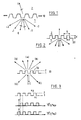
- GIRO-gratings The working scheme of GIRO-gratings is set out, with geometry and notations shown in figure 3 .
- a linearly polarised plane wave with free space wavelength ⁇ is incident on a grating with linear groves with period ⁇ , layer thickness d, and fill factor f, from a homogeneous medium with refractive index n 1 .
- the incident optical power can couple to the following waves: zero order in transmission (a), higher orders in transmission (b), zero order in reflection (c) and higher orders in reflection (d).
- a problem consists in how to cancel all unwanted diffraction orders (all except (c)), thereby forcing all optical power to couple to the specular reflection, i.e. beam (c).
- the grating parameters are chosen such that after reflection at interface 2, the backpropagating field interferes constructively with the primary reflection at interface 1, and the total reflected field exhibits a constant phase, thereby preventing coupling to uneven diffraction orders.
- the grating period is chosen such that only three propagation modes are supported in the grating regions, with respective field profiles ⁇ 0 (x), ⁇ 1 (x) and ⁇ 2 (x) and effective indices n e,0 , n e,1 and n e,3 . Due to the uneven symmetry of mode 1, no optical power is coupled from the incident beam to this mode.
- RCWA results are given in table 2 hereafter wherein the subscript "appr” refers to the start values and optimum values are indicated with the subscript "opt”.
- the fraction of the incident optical power coupled to the desired zero order in reflection is given for the optimum parameter set.
- Table 2 shows a comparison of GIRO-grating design based on expressions presented herein and optimisation based on RCWA.
- Parameters of the optimised GIRO-grating are: grating period 930 nm, grating depth 465 nm and grating fill factor 50%.
- Reflectivity for the TM and TE zero orders are shown in figure 4 with results obtained by RCWA modelling.
- the TM-reflectivity amounts to 99,9% while the TE-reflectivity is as low as 2,0%. This indicates that the use of GIRO-gratings also may offer a possibility to solve the VCSEL-problem of polarisation instability.
- GIRO-gratings designed for operation at a wavelength of 10,6 ⁇ m, which is the wavelength range of CO 2 -lasers, with reference to figure 5 .
- GIRO structure for operation at a wavelength of 10,6 ⁇ m is set out hereafter.
- the component consists of a linear grating 50, with rectangular grooves 53, etched into a GaAs substrate 51.
- the geometry is designed such that the zero-order reflectivity for on-axis incidence is maximised for a TM-polarised plane wave whereby TM-polarisation means incident electrical field vector 54 perpendicular to the grating grooves 53. This plane wave is incident from the substrate side 51, and is consequently reflected back 55 into the substrate 51.
- Grating filling factor f is defined as the percentage of grating material in one grating period.
- a set-up as schematically shown in Fig. 6 was used.
- a CO 2 -laser beam 64 is incident upon a beam splitter 61.
- Part of the optical power is coupled directly to a detector 62 for calibration purposes, and the other part is coupled to another detector 63 after reflection on the sample 60.
- the backside of the samples are angle-polished, as shown in figure 7 , e.g. with a typical polishing angle of 3,5°.
- This approach allow separate measurement of frontside and backside sample reflectivity, while avoiding interference through multiple reflections inside the GIRO-sample 70, which would severely complicate the measurement interpretation.
- Measuring the optical power in the frontside and backside primary reflected beams 71, resp. 72, in combination with monitoring the incident optical power, allows to derive the GIRO-grating reflectivity in absolute terms 73.
Landscapes
- Physics & Mathematics (AREA)
- General Physics & Mathematics (AREA)
- Optics & Photonics (AREA)
- Condensed Matter Physics & Semiconductors (AREA)
- Electromagnetism (AREA)
- Optical Integrated Circuits (AREA)
- Optical Elements Other Than Lenses (AREA)
- Diffracting Gratings Or Hologram Optical Elements (AREA)
Claims (10)
- Verfahren zur Gestaltung eines Systems zur Reflexion eines Strahls einer elektromagnetischen Strahlung mit einer vorbestimmten Vakuumwellenlänge (λ) und linearer Polarisation, der im Wesentlichen rechtwinklig einfällt auf eine Gitterschicht des Systems, für mehr als 90 % in der spektralen Reflexion nullter Ordnung, wobei das System Folgendes aufweist:- ein erstes dielektrisches Medium (1) mit einer ersten Brechzahl (n1), in das der Strahl einfällt;- ein zweites dielektrisches Medium (2) mit einer zweiten Brechzahl (n2), wobei n2 n1; und- ein Gitter (10, 20, ...70) mit linearen Furchen zwischen dem ersten und dem zweiten Medium, wobei das Gitter aus dem ersten Medium (1) gebildet wird und eine Gitterperiode (Λ), eine Gitterdicke (d) und einen Füllfaktor (f) aufweist;wobei das Verfahren den Schritt umfasst, eine Gitterperiode zu wählen, die geringer ist als die Wellenlänge der elektromagnetischen Strahlung im zweiten dielektrischen Medium (Λ <λ/n2),
dadurch gekennzeichnet, dass das Verfahren zusätzlich den Schritt umfasst, die Gitterperiode (Λ), die Gitterdicke (d) und den Füllfaktor (f) mithilfe folgender Gestaltungsregeln zu bestimmen:
- Verfahren nach Anspruch 1, dadurch gekennzeichnet, dass das Gitter eine ausreichend große Variation der dielektrischen Eigenschaften innerhalb einer Wiederholung der Periode aufweist, damit der Strahl beim Einfallen auf die dielektrische Schicht in dieser Schicht mindestens zwei Ausbreitungsmodi erzeugt.
- Verfahren nach Anspruch 1 oder 2, dadurch gekennzeichnet, dass das Gitter eine periodische Struktur in mehreren Richtungen aufweist, wobei die periodische Struktur eine Periode (A) in jeder dieser Richtungen aufweist, die kleiner ist als die Wellenlänge der elektromagnetischen Strahlung im zweiten dielektrischen Medium (2).
- Verfahren nach Anspruch 1 oder 2, dadurch gekennzeichnet, dass das Gitter (10,...) eine eindimensionale Periodizität aufweist.
- Verfahren nach einem der Ansprüche 1 bis 4, dadurch gekennzeichnet, dass ein TM-Polarisationsmodus der einfallenden Welle festgelegt wird.
- Verfahren nach einem der Ansprüche 1 bis 4, dadurch gekennzeichnet, dass ein TE-Polarisationsmodus der einfallenden Welle festgelegt wird.
- Verfahren nach einem der Ansprüche 1 bis 6, dadurch gekennzeichnet, dass das Gitter (20, 30, 50) einen im Wesentlichen rechteckigen Querschnitt aufweist.
- Verfahren nach einem der Ansprüche 1 bis 7, dadurch gekennzeichnet, dass das zweite Medium (2) durch Luft oder Vakuum mit einer zweiten Brechzahl (n2) von annähernd bis Eins gebildet wird,
wobei die Gitterperiode (Λ) und die Gitterdicke (d) mithilfe folgender Gestaltungsregeln bestimmt werden:

wobei (n0,eff) die effektive Brechzahl des Gitters bezeichnet. - Verfahren nach Anspruch 8, dadurch gekennzeichnet, dass die erste Brechzahl (n1) innerhalb eines Bereichs von 3 bis 4, vorzugsweise ungefähr 3,5, gewählt wird.
- Verfahren nach einem der Ansprüche 1 bis 9, dadurch gekennzeichnet, dass es sich bei dem Strahl um einen CO2-Laser-Strahl handelt.
Applications Claiming Priority (4)
| Application Number | Priority Date | Filing Date | Title |
|---|---|---|---|
| BE9600280A BE1010069A6 (nl) | 1996-03-29 | 1996-03-29 | Optisch systeem met hoge reflectiviteitsrooster. |
| BE9600280 | 1996-03-29 | ||
| US1645496P | 1996-04-29 | 1996-04-29 | |
| US16454 | 1996-04-29 |
Publications (3)
| Publication Number | Publication Date |
|---|---|
| EP0798574A2 EP0798574A2 (de) | 1997-10-01 |
| EP0798574A3 EP0798574A3 (de) | 1998-09-02 |
| EP0798574B1 true EP0798574B1 (de) | 2008-05-14 |
Family
ID=3889642
Family Applications (1)
| Application Number | Title | Priority Date | Filing Date |
|---|---|---|---|
| EP97870045A Expired - Lifetime EP0798574B1 (de) | 1996-03-29 | 1997-04-01 | Optisches System mit einer hochreflektierenden, polarisationsselektiven, dielektrischen Struktur mit Abmessung kleiner als die Wellenlänge |
Country Status (4)
| Country | Link |
|---|---|
| US (1) | US6191890B1 (de) |
| EP (1) | EP0798574B1 (de) |
| BE (1) | BE1010069A6 (de) |
| DE (1) | DE69738679D1 (de) |
Families Citing this family (68)
| Publication number | Priority date | Publication date | Assignee | Title |
|---|---|---|---|---|
| DE10353951A1 (de) * | 2003-11-18 | 2005-06-16 | U-L-M Photonics Gmbh | Polarisationskontrolle von Vertikaldiodenlasern durch ein monolothisch integriertes Oberflächengitter |
| GB9916145D0 (en) * | 1999-07-10 | 1999-09-08 | Secr Defence | Control of polarisation of vertical cavity surface emitting lasers |
| DE60035420T2 (de) * | 1999-08-02 | 2008-03-06 | Université Jean Monnet | Optische polarisationsvorrichtung und polarisationsvorrichtung zum gebrauch mit einem laser |
| EP1868015B1 (de) * | 1999-08-02 | 2012-04-18 | Université Jean-Monnet | Optische Polarisationsvorrichtung und Polarisationsvorrichtung zum Gebrauch mit einem Laser |
| US6680799B1 (en) | 1999-08-02 | 2004-01-20 | Universite Jean Monnet | Optical polarizing device and laser polarization device |
| US8111401B2 (en) * | 1999-11-05 | 2012-02-07 | Robert Magnusson | Guided-mode resonance sensors employing angular, spectral, modal, and polarization diversity for high-precision sensing in compact formats |
| US7167615B1 (en) | 1999-11-05 | 2007-01-23 | Board Of Regents, The University Of Texas System | Resonant waveguide-grating filters and sensors and methods for making and using same |
| US6597721B1 (en) * | 2000-09-21 | 2003-07-22 | Ut-Battelle, Llc | Micro-laser |
| US6990135B2 (en) * | 2002-10-28 | 2006-01-24 | Finisar Corporation | Distributed bragg reflector for optoelectronic device |
| US6905900B1 (en) * | 2000-11-28 | 2005-06-14 | Finisar Corporation | Versatile method and system for single mode VCSELs |
| US7065124B2 (en) * | 2000-11-28 | 2006-06-20 | Finlsar Corporation | Electron affinity engineered VCSELs |
| US6836501B2 (en) * | 2000-12-29 | 2004-12-28 | Finisar Corporation | Resonant reflector for increased wavelength and polarization control |
| TWI227799B (en) * | 2000-12-29 | 2005-02-11 | Honeywell Int Inc | Resonant reflector for increased wavelength and polarization control |
| WO2003025635A1 (en) * | 2001-09-19 | 2003-03-27 | Technion Research & Development Foundation Ltd. | Space-variant subwavelength dielectric grating and applications thereof |
| US6747799B2 (en) * | 2001-11-12 | 2004-06-08 | Pts Corporation | High-efficiency low-polarization-dependent-loss lamellar diffraction-grating profile and production process |
| US6876784B2 (en) * | 2002-05-30 | 2005-04-05 | Nanoopto Corporation | Optical polarization beam combiner/splitter |
| US7386205B2 (en) * | 2002-06-17 | 2008-06-10 | Jian Wang | Optical device and method for making same |
| US7283571B2 (en) * | 2002-06-17 | 2007-10-16 | Jian Wang | Method and system for performing wavelength locking of an optical transmission source |
| JP4310080B2 (ja) * | 2002-06-17 | 2009-08-05 | キヤノン株式会社 | 回折光学素子およびこれを備えた光学系、光学装置 |
| US20040047039A1 (en) * | 2002-06-17 | 2004-03-11 | Jian Wang | Wide angle optical device and method for making same |
| AU2003267964A1 (en) | 2002-06-18 | 2003-12-31 | Nanoopto Corporation | Optical components exhibiting enhanced functionality and method of making same |
| EP1535106A4 (de) | 2002-08-01 | 2009-01-07 | Api Nanofabrication And Res Co | Präzisionsphasenverzögerungsvorrichtung und deren herstellungsverfahren |
| US7064899B2 (en) * | 2002-08-30 | 2006-06-20 | Digital Optics Corp. | Reduced loss diffractive structure |
| US6965626B2 (en) * | 2002-09-03 | 2005-11-15 | Finisar Corporation | Single mode VCSEL |
| US7190521B2 (en) * | 2002-09-13 | 2007-03-13 | Technion Research And Development Foundation Ltd. | Space-variant subwavelength dielectric grating and applications thereof |
| US6661830B1 (en) | 2002-10-07 | 2003-12-09 | Coherent, Inc. | Tunable optically-pumped semiconductor laser including a polarizing resonator mirror |
| US6920272B2 (en) * | 2002-10-09 | 2005-07-19 | Nanoopto Corporation | Monolithic tunable lasers and reflectors |
| US7013064B2 (en) * | 2002-10-09 | 2006-03-14 | Nanoopto Corporation | Freespace tunable optoelectronic device and method |
| US6813293B2 (en) * | 2002-11-21 | 2004-11-02 | Finisar Corporation | Long wavelength VCSEL with tunnel junction, and implant |
| WO2004079410A1 (en) * | 2003-01-06 | 2004-09-16 | Polychromix Corporation | Diffraction grating having high throughput effiency |
| WO2004072692A2 (en) * | 2003-02-10 | 2004-08-26 | Nanoopto Corporation | Universal broadband polarizer, devices incorporating same, and method of making same |
| JPWO2004081620A1 (ja) * | 2003-03-13 | 2006-06-15 | 旭硝子株式会社 | 回折素子および光学装置 |
| US20040222363A1 (en) * | 2003-05-07 | 2004-11-11 | Honeywell International Inc. | Connectorized optical component misalignment detection system |
| US20040247250A1 (en) * | 2003-06-03 | 2004-12-09 | Honeywell International Inc. | Integrated sleeve pluggable package |
| US7298942B2 (en) | 2003-06-06 | 2007-11-20 | Finisar Corporation | Pluggable optical optic system having a lens fiber stop |
| US20040258355A1 (en) * | 2003-06-17 | 2004-12-23 | Jian Wang | Micro-structure induced birefringent waveguiding devices and methods of making same |
| US7433381B2 (en) | 2003-06-25 | 2008-10-07 | Finisar Corporation | InP based long wavelength VCSEL |
| US7054345B2 (en) | 2003-06-27 | 2006-05-30 | Finisar Corporation | Enhanced lateral oxidation |
| US7277461B2 (en) * | 2003-06-27 | 2007-10-02 | Finisar Corporation | Dielectric VCSEL gain guide |
| US7075962B2 (en) * | 2003-06-27 | 2006-07-11 | Finisar Corporation | VCSEL having thermal management |
| US6961489B2 (en) | 2003-06-30 | 2005-11-01 | Finisar Corporation | High speed optical system |
| US7149383B2 (en) * | 2003-06-30 | 2006-12-12 | Finisar Corporation | Optical system with reduced back reflection |
| US20060056762A1 (en) * | 2003-07-02 | 2006-03-16 | Honeywell International Inc. | Lens optical coupler |
| US20050013542A1 (en) * | 2003-07-16 | 2005-01-20 | Honeywell International Inc. | Coupler having reduction of reflections to light source |
| US7210857B2 (en) * | 2003-07-16 | 2007-05-01 | Finisar Corporation | Optical coupling system |
| US20050013539A1 (en) * | 2003-07-17 | 2005-01-20 | Honeywell International Inc. | Optical coupling system |
| US6887801B2 (en) * | 2003-07-18 | 2005-05-03 | Finisar Corporation | Edge bead control method and apparatus |
| US7031363B2 (en) * | 2003-10-29 | 2006-04-18 | Finisar Corporation | Long wavelength VCSEL device processing |
| US7920612B2 (en) * | 2004-08-31 | 2011-04-05 | Finisar Corporation | Light emitting semiconductor device having an electrical confinement barrier near the active region |
| US7829912B2 (en) * | 2006-07-31 | 2010-11-09 | Finisar Corporation | Efficient carrier injection in a semiconductor device |
| US7596165B2 (en) * | 2004-08-31 | 2009-09-29 | Finisar Corporation | Distributed Bragg Reflector for optoelectronic device |
| US7859753B2 (en) * | 2005-12-21 | 2010-12-28 | Chem Image Corporation | Optical birefringence filters with interleaved absorptive and zero degree reflective polarizers |
| US8590271B2 (en) * | 2006-04-13 | 2013-11-26 | Sabic Innovative Plastics Ip B.V. | Multi-wall structural components having enhanced radiatransmission capability |
| US7992361B2 (en) * | 2006-04-13 | 2011-08-09 | Sabic Innovative Plastics Ip B.V. | Polymer panels and methods of making the same |
| US20070242715A1 (en) * | 2006-04-18 | 2007-10-18 | Johan Gustavsson | Mode and polarization control in vcsels using sub-wavelength structure |
| US8031752B1 (en) | 2007-04-16 | 2011-10-04 | Finisar Corporation | VCSEL optimized for high speed data |
| US9306290B1 (en) * | 2007-05-31 | 2016-04-05 | Foersvarets Materielverk | Controller barrier layer against electromagnetic radiation |
| DE102007033567A1 (de) | 2007-07-19 | 2009-04-09 | Trumpf Laser- Und Systemtechnik Gmbh | Phasenschiebe-Einrichtung und Laserresonator zur Erzeugung radial oder azimutal polarisierter Laserstrahlung |
| US8126694B2 (en) * | 2008-05-02 | 2012-02-28 | Nanometrics Incorporated | Modeling conductive patterns using an effective model |
| DE102008030374B4 (de) | 2008-06-26 | 2014-09-11 | Trumpf Laser- Und Systemtechnik Gmbh | Verfahren zum Laserschneiden und CO2-Laserschneidmaschine |
| EP2141519A1 (de) | 2008-07-04 | 2010-01-06 | Université Jean-Monnet | Polarisierender Spiegel mit diffraktiver Oberfläche |
| DE102009001505A1 (de) | 2008-11-21 | 2010-05-27 | Vertilas Gmbh | Oberflächenemittierende Halbleiterlaserdiode und Verfahren zur Herstellung derselben |
| US9357240B2 (en) | 2009-01-21 | 2016-05-31 | The Nielsen Company (Us), Llc | Methods and apparatus for providing alternate media for video decoders |
| US8270814B2 (en) | 2009-01-21 | 2012-09-18 | The Nielsen Company (Us), Llc | Methods and apparatus for providing video with embedded media |
| FR2945159B1 (fr) * | 2009-04-29 | 2016-04-01 | Horiba Jobin Yvon Sas | Reseau de diffraction metallique en reflexion a haute tenue au flux en regime femtoseconde, systeme comprenant un tel reseau et procede d'amelioration du seuil d'endommagement d'un reseau de diffraction metallique |
| WO2011044439A1 (en) * | 2009-10-08 | 2011-04-14 | The Penn State Research Foundation | Multi-spectral filters, mirrors and antireflective coatings with subwavelength periodic features for optical devices |
| FR2979436B1 (fr) * | 2011-08-29 | 2014-02-07 | Commissariat Energie Atomique | Dispositif reflecteur pour face arriere de dispositifs optiques |
| JP6811448B2 (ja) * | 2016-09-14 | 2021-01-13 | 日本電気株式会社 | グレーティングカプラ |
Family Cites Families (7)
| Publication number | Priority date | Publication date | Assignee | Title |
|---|---|---|---|---|
| JPS58174906A (ja) * | 1982-04-07 | 1983-10-14 | Ricoh Co Ltd | 光学素子の表面反射防止法 |
| EP0322714B1 (de) * | 1987-12-24 | 1996-09-11 | Kuraray Co., Ltd. | Polarisierendes optisches Element und Einrichtung unter Benutzung desselben |
| JPH02178604A (ja) * | 1988-12-28 | 1990-07-11 | Kuraray Co Ltd | 交差回折格子およびこれを用いた偏波回転検出装置 |
| JP2961964B2 (ja) | 1991-07-10 | 1999-10-12 | 日本電気株式会社 | 半導体レーザ装置 |
| JPH09500459A (ja) * | 1994-05-02 | 1997-01-14 | フィリップス エレクトロニクス ネムローゼ フェンノートシャップ | 反射防止回折格子を有する光透過性光学素子 |
| US5598300A (en) * | 1995-06-05 | 1997-01-28 | Board Of Regents, The University Of Texas System | Efficient bandpass reflection and transmission filters with low sidebands based on guided-mode resonance effects |
| US5726805A (en) * | 1996-06-25 | 1998-03-10 | Sandia Corporation | Optical filter including a sub-wavelength periodic structure and method of making |
-
1996
- 1996-03-29 BE BE9600280A patent/BE1010069A6/nl not_active IP Right Cessation
-
1997
- 1997-03-31 US US08/829,348 patent/US6191890B1/en not_active Expired - Lifetime
- 1997-04-01 DE DE69738679T patent/DE69738679D1/de not_active Expired - Lifetime
- 1997-04-01 EP EP97870045A patent/EP0798574B1/de not_active Expired - Lifetime
Non-Patent Citations (1)
| Title |
|---|
| WANG S S; MAGNUSSON R: "MULTILAYER WAVEGUIDE-GRATING FILTERS", APPLIED OPTICS, OSA, OPTICAL SOCIETY OF AMERICA, 10 May 1995 (1995-05-10), WASHINGTON, DC, US, pages 2414 - 2420, XP000511437 * |
Also Published As
| Publication number | Publication date |
|---|---|
| US6191890B1 (en) | 2001-02-20 |
| EP0798574A3 (de) | 1998-09-02 |
| BE1010069A6 (nl) | 1997-12-02 |
| DE69738679D1 (de) | 2008-06-26 |
| EP0798574A2 (de) | 1997-10-01 |
Similar Documents
| Publication | Publication Date | Title |
|---|---|---|
| EP0798574B1 (de) | Optisches System mit einer hochreflektierenden, polarisationsselektiven, dielektrischen Struktur mit Abmessung kleiner als die Wellenlänge | |
| Lalanne et al. | Bloch-wave engineering for high-Q, small-V microcavities | |
| Sharon et al. | Narrow spectral bandwidths with grating waveguide structures | |
| Lalanne et al. | Optical properties of deep lamellar gratings: a coupled Bloch-mode insight | |
| EP2715417B1 (de) | Planarer gitter-polarisationswandler | |
| Palamaru et al. | Photonic crystal waveguides: Out-of-plane losses and adiabatic modal conversion | |
| US8442374B2 (en) | Ultra-low loss hollow core waveguide using high-contrast gratings | |
| US20100091369A1 (en) | Double-layer grating | |
| Levy-Yurista et al. | Very narrow spectral filters with multilayered grating-waveguide structures | |
| EP1194988A1 (de) | Polarisationsregelung von oberflächenemittierenden lasern mit vertikalem resonator | |
| EP2300858A1 (de) | Polarisierendes brechungsspiegelgerät | |
| JP7438283B2 (ja) | 非線形周波数変換素子を有する、ヘテロジニアスに統合したフォトニックプラットフォーム | |
| Sang et al. | Resonant excitation analysis on asymmetrical lateral leakage of light in finite zero-contrast grating mirror | |
| Rowe et al. | High-reflectivity surface-relief gratings in single-mode optical fibres | |
| Schmid et al. | Subwavelength grating structures in planar waveguide facets for modified reflectivity | |
| JP2004505309A (ja) | 光学導波管フィルタ | |
| Kintaka et al. | Thin-film narrowband retroreflector based on waveguide grating structure | |
| Kleckner et al. | Design, fabrication, and characterization of deep-etched waveguide gratings | |
| EP1198726B1 (de) | Optische polarisationsvorrichtung und polarisationsvorrichtung zum gebrauch mit einem laser | |
| Kawashima et al. | Photonic crystal polarization beam splitters and their applications: first industrialization of photonic crystal devices | |
| EP1868015B1 (de) | Optische Polarisationsvorrichtung und Polarisationsvorrichtung zum Gebrauch mit einem Laser | |
| Magnusson et al. | Spectral-band engineering with interacting resonant leaky modes in thin periodic films | |
| Levy-Yurista et al. | Dual spectral filters with multi-layered grating waveguide structures | |
| Bonnet et al. | Resonant grating effects at terahertz frequencies | |
| Buus et al. | Transmission characteristics of fibre gratings |
Legal Events
| Date | Code | Title | Description |
|---|---|---|---|
| PUAI | Public reference made under article 153(3) epc to a published international application that has entered the european phase |
Free format text: ORIGINAL CODE: 0009012 |
|
| AK | Designated contracting states |
Kind code of ref document: A2 Designated state(s): BE DE FR GB IT NL SE |
|
| PUAL | Search report despatched |
Free format text: ORIGINAL CODE: 0009013 |
|
| AK | Designated contracting states |
Kind code of ref document: A3 Designated state(s): BE DE FR GB IT NL SE |
|
| 17P | Request for examination filed |
Effective date: 19990225 |
|
| 17Q | First examination report despatched |
Effective date: 20020923 |
|
| RIC1 | Information provided on ipc code assigned before grant |
Ipc: 7H 01S 3/085 A |
|
| GRAP | Despatch of communication of intention to grant a patent |
Free format text: ORIGINAL CODE: EPIDOSNIGR1 |
|
| RIC1 | Information provided on ipc code assigned before grant |
Ipc: H01S 5/183 20060101ALI20070516BHEP Ipc: G02B 5/18 20060101AFI20070516BHEP |
|
| GRAS | Grant fee paid |
Free format text: ORIGINAL CODE: EPIDOSNIGR3 |
|
| GRAA | (expected) grant |
Free format text: ORIGINAL CODE: 0009210 |
|
| AK | Designated contracting states |
Kind code of ref document: B1 Designated state(s): BE DE FR GB IT NL SE |
|
| REG | Reference to a national code |
Ref country code: GB Ref legal event code: FG4D |
|
| REF | Corresponds to: |
Ref document number: 69738679 Country of ref document: DE Date of ref document: 20080626 Kind code of ref document: P |
|
| NLV1 | Nl: lapsed or annulled due to failure to fulfill the requirements of art. 29p and 29m of the patents act | ||
| PG25 | Lapsed in a contracting state [announced via postgrant information from national office to epo] |
Ref country code: NL Free format text: LAPSE BECAUSE OF FAILURE TO SUBMIT A TRANSLATION OF THE DESCRIPTION OR TO PAY THE FEE WITHIN THE PRESCRIBED TIME-LIMIT Effective date: 20080514 |
|
| PG25 | Lapsed in a contracting state [announced via postgrant information from national office to epo] |
Ref country code: SE Free format text: LAPSE BECAUSE OF FAILURE TO SUBMIT A TRANSLATION OF THE DESCRIPTION OR TO PAY THE FEE WITHIN THE PRESCRIBED TIME-LIMIT Effective date: 20080814 |
|
| PG25 | Lapsed in a contracting state [announced via postgrant information from national office to epo] |
Ref country code: BE Free format text: LAPSE BECAUSE OF FAILURE TO SUBMIT A TRANSLATION OF THE DESCRIPTION OR TO PAY THE FEE WITHIN THE PRESCRIBED TIME-LIMIT Effective date: 20080514 |
|
| PLBE | No opposition filed within time limit |
Free format text: ORIGINAL CODE: 0009261 |
|
| STAA | Information on the status of an ep patent application or granted ep patent |
Free format text: STATUS: NO OPPOSITION FILED WITHIN TIME LIMIT |
|
| 26N | No opposition filed |
Effective date: 20090217 |
|
| PG25 | Lapsed in a contracting state [announced via postgrant information from national office to epo] |
Ref country code: IT Free format text: LAPSE BECAUSE OF FAILURE TO SUBMIT A TRANSLATION OF THE DESCRIPTION OR TO PAY THE FEE WITHIN THE PRESCRIBED TIME-LIMIT Effective date: 20080514 |
|
| PGFP | Annual fee paid to national office [announced via postgrant information from national office to epo] |
Ref country code: GB Payment date: 20140327 Year of fee payment: 18 |
|
| PGFP | Annual fee paid to national office [announced via postgrant information from national office to epo] |
Ref country code: DE Payment date: 20140321 Year of fee payment: 18 Ref country code: FR Payment date: 20140422 Year of fee payment: 18 |
|
| REG | Reference to a national code |
Ref country code: DE Ref legal event code: R119 Ref document number: 69738679 Country of ref document: DE |
|
| GBPC | Gb: european patent ceased through non-payment of renewal fee |
Effective date: 20150401 |
|
| PG25 | Lapsed in a contracting state [announced via postgrant information from national office to epo] |
Ref country code: DE Free format text: LAPSE BECAUSE OF NON-PAYMENT OF DUE FEES Effective date: 20151103 Ref country code: GB Free format text: LAPSE BECAUSE OF NON-PAYMENT OF DUE FEES Effective date: 20150401 |
|
| REG | Reference to a national code |
Ref country code: FR Ref legal event code: ST Effective date: 20151231 |
|
| PG25 | Lapsed in a contracting state [announced via postgrant information from national office to epo] |
Ref country code: FR Free format text: LAPSE BECAUSE OF NON-PAYMENT OF DUE FEES Effective date: 20150430 |