EP0797189A1 - Herstellungsverfahren eines Magnetkopfs mit Magnetowiderstandselement und nach diesem Verfahren erhaltener Kopf - Google Patents
Herstellungsverfahren eines Magnetkopfs mit Magnetowiderstandselement und nach diesem Verfahren erhaltener Kopf Download PDFInfo
- Publication number
- EP0797189A1 EP0797189A1 EP97400296A EP97400296A EP0797189A1 EP 0797189 A1 EP0797189 A1 EP 0797189A1 EP 97400296 A EP97400296 A EP 97400296A EP 97400296 A EP97400296 A EP 97400296A EP 0797189 A1 EP0797189 A1 EP 0797189A1
- Authority
- EP
- European Patent Office
- Prior art keywords
- layer
- magnetic
- wall
- insulating
- stack
- Prior art date
- Legal status (The legal status is an assumption and is not a legal conclusion. Google has not performed a legal analysis and makes no representation as to the accuracy of the status listed.)
- Withdrawn
Links
Images


Classifications
-
- G—PHYSICS
- G11—INFORMATION STORAGE
- G11B—INFORMATION STORAGE BASED ON RELATIVE MOVEMENT BETWEEN RECORD CARRIER AND TRANSDUCER
- G11B5/00—Recording by magnetisation or demagnetisation of a record carrier; Reproducing by magnetic means; Record carriers therefor
- G11B5/127—Structure or manufacture of heads, e.g. inductive
- G11B5/33—Structure or manufacture of flux-sensitive heads, i.e. for reproduction only; Combination of such heads with means for recording or erasing only
- G11B5/39—Structure or manufacture of flux-sensitive heads, i.e. for reproduction only; Combination of such heads with means for recording or erasing only using magneto-resistive devices or effects
- G11B5/3903—Structure or manufacture of flux-sensitive heads, i.e. for reproduction only; Combination of such heads with means for recording or erasing only using magneto-resistive devices or effects using magnetic thin film layers or their effects, the films being part of integrated structures
-
- G—PHYSICS
- G11—INFORMATION STORAGE
- G11B—INFORMATION STORAGE BASED ON RELATIVE MOVEMENT BETWEEN RECORD CARRIER AND TRANSDUCER
- G11B5/00—Recording by magnetisation or demagnetisation of a record carrier; Reproducing by magnetic means; Record carriers therefor
- G11B5/127—Structure or manufacture of heads, e.g. inductive
- G11B5/31—Structure or manufacture of heads, e.g. inductive using thin films
- G11B5/3163—Fabrication methods or processes specially adapted for a particular head structure, e.g. using base layers for electroplating, using functional layers for masking, using energy or particle beams for shaping the structure or modifying the properties of the basic layers
Definitions
- the subject of the present invention is a method for producing a magnetic head with a magnetoresistive element and a magnetic head obtained by this method.
- Magnetic heads are known which are produced in a so-called horizontal thin film technique. Such heads are described in document FR-A-2,645,314 (or in its American correspondent US-A-5,208,716). A head of this kind is shown in Figure 1 attached.
- a horizontal head comprising a semiconductor substrate 10, for example made of silicon, in which a box 12 has been etched.
- a lower magnetic layer 14 has been formed electrolytically and has been extended by two pillars 16 1 , 16 2 .
- a conductive winding 18 surrounds the pillars.
- This coil is embedded in an insulating layer 20.
- the magnetic circuit is completed by an upper magnetic part comprising two pole pieces 22 1 , 22 2 separated by a non-magnetic spacer 24.
- a magnetoresistive element MR by example in iron-nickel, is arranged under the non-magnetic spacer 24, in the insulator 20.
- the head moves in front of a magnetic support 30 where the information to be read or written is recorded.
- the current flowing in the winding 18 creates a magnetic field and, consequently, an induction in the magnetic circuit.
- the field lines which open out around the spacer induce a magnetization in the support 30.
- magnetic information recorded in the support 30 produces a magnetic reading field and, consequently, an induction in the magnetic circuit.
- This induction closes, in part, through the magnetoresistive element MR.
- a variant of these heads consists in adding between the pillars and the pole pieces two magnetic pieces constituting flux concentrators. Such heads are described in FR-A-2 712 420 and in FR-A-2 709 855.
- the object of the invention is precisely to solve this double technical problem.
- the invention proposes a method of producing a magnetic head which makes it possible to place the magnetoresistive element in the air gap itself, that is to say between the two pole pieces and no longer under the level of these. Furthermore, the method allows automatic alignment of the magnetoresistive element with respect to the air gap.
- a wall is formed which comprises only a non-magnetic wall.
- the width of the magnetoresistive element remaining after etching is then equal to that of the non-magnetic spacer.
- a wall is formed which comprises two vertical walls of insulating material framing a vertical wall of non-magnetic material, and, after having etched the stack of layers using these three walls as a mask, the two vertical insulating walls on either side of the non-magnetic wall to leave only the non-magnetic wall. The width of the magnetoresistant element remaining is then greater than that of the non-magnetic spacer.
- the present invention also relates to a magnetic head obtained by this process.
- This head is of the type which includes a magnetic circuit with two pole pieces separated by a non-magnetic spacer and a magnetoresistive element.
- the head of the invention is characterized in that the magnetoresistive element is located between the two pole pieces and is self-aligned with the non-magnetic spacer.
- This sub-assembly comprises a lower magnetic part 14, two magnetic pillars 16 1 , 16 2 and two concentrators 32 1 , 32 2 .
- a conductive winding 18 surrounds the pillars 16 1 , 16 2 .
- the assembly is embedded in an insulator 20.
- This sub-assembly has a flat upper surface 34, on which different layers will be deposited and etched according to the invention.
- the first layer 41 of conductive material, must have good adhesion, and must be selectively etched with respect to an insulator such as silica. Many materials can be used for this purpose, such as tungsten, chromium, titanium, etc. In the following, we will assume that we have chosen tungsten.
- the thickness of this layer can be a fraction of a micrometer.
- the material of the second layer 42 must be able to be etched selectively with respect to the metal sublayer 41. It can be, for example, silica SiO 2 . It is on this insulating layer, for example made of silica, that the layer which will constitute the magnetoresistive element is deposited. This layer can be of any material magnetoresistive. They may in particular be multilayers.
- the second insulating layer 44 may be identical to the first, 42, and the second metal layer 45 identical to the first, 41, that is to say respectively of silica and tungsten, for example.
- an insulating layer 50 for example of resin, a few micrometers thick, is deposited.
- a step 52 is engraved with a riser 54, as illustrated in FIG. 5.
- a thin layer of insulator 56 is then deposited, for example by LPCVD ("Low Pressure Chemical Vapor Deposition"). This layer is deposited on horizontal surfaces, but also on the vertical riser. The thickness of this layer must correspond to the length of the future air gap, (that is to say to its dimension taken in the direction of movement of the recording medium).
- LPCVD Low Pressure Chemical Vapor Deposition
- the layer 56 is etched, to make the horizontal parts disappear but leave a vertical wall 60 on the riser, as illustrated in FIG. 7.
- the upper metal layer 45 serves stop layer.
- the resin step 52 is then removed and a vertical wall 60 is obtained as illustrated in FIG. 8.
- the stack of layers 40 is then attacked, with the exception of the first metallic layer 41.
- the second metal layer 45 is thus etched, which is made of tungsten for example; then, by changing the etching method, the second insulating layer 44 is etched, which is for example made of SiO 2 ; the etching method is further changed to etch the layer of magnetoresistive material 43; the etching specific to the insulating material is resumed to etch the first insulating layer 42, and one stops on the first metallic layer 41, which is for example made of tungsten.
- FIG. 9 We then obtain the assembly illustrated in FIG. 9 where we see under the wall 60, an engraved stack 62 comprising a first insulating tape 64, a magnetoresistive tape MR, a second insulating tape 66 and a metal tape 68. of its mode of obtaining by etching the wall 60 being taken as a mask, the assembly 62, therefore the element MR, is automatically aligned with respect to the wall.
- a layer of insulation (resin, silica, etc.) is then deposited with a thickness greater than the thickness of the stack 62, and this layer is etched , for example in oxygen plasma. There then remain, on the flanks of the engraved stack, layers 70 1 , 70 2 shown in FIG. 10.
- the two pole pieces 72 1 , 72 2 can be made of iron-nickel for example.
- the magnetoresistive element MR which is placed by construction, above the first metallic layer 41, is found situated above the lower level of the pole pieces, in other words between the pole pieces and no longer under those -this, as in the prior art. This arrangement is very favorable to the operation of reading the recording, since the magnetic field lines will borrow the magnetoresistive element more effectively.
- the width of the magnetoresistive element is less than or equal to the dimension of the non-magnetic gap counted in the direction of movement of the recording medium (dimension which is generally names "length").
- dimension which is generally names "length” dimension which is generally names "length"
- the invention is not limited to this particular case and also encompasses the case where the width of the magnetoresistive element is greater than the length of the air gap. This second mode of implementation is illustrated in FIGS. 13 to 21.
- a material meeting these requirements is polycrystalline silicon. This material can be deposited either by sputtering or by LPCVD with good market coverage.
- the layer 82 which can therefore be made of polycrystalline silicon, has a thickness on the flank of between approximately 0.1 microns and a few microns.
- This layer 82 is then etched vertically by stopping on the second metal layer 45 and a first vertical wall 84 is obtained as shown in FIG. 14.
- an insulating layer 86 for example of silica SiO 2 , whose thickness along the vertical wall is equal to the length of the future air gap.
- the layer 86 is etched vertically, stopping again on the second metal layer 45. This then gives a second vertical wall 86 pressed against the side of the first, 84.
- a layer of a material identical to that of layer 82 is deposited again, therefore for example in polycrystalline silicon and, after vertical etching as in FIG. 14, a third wall is obtained vertical 88 in silicon.
- the three walls are shown in Figure 16.
- the second wall 86 constitutes the future non-magnetic spacer.
- this set of three vertical walls 84, 86, 88 is then used as a mask for etching the initial stack 40 of metallic, insulating and magnetoresistive layers by taking the first metallic layer 41 as layer d 'stop.
- the arrangement illustrated in FIG. 17 is then obtained, where the engraved stack bears the reference 90.
- This engraved stack is composed of a first insulating tape 92, a magnetoresistive tape MR and a second magnetoresistant tape 96.
- This stack has naturally a width equal to that of all three vertical walls 84, 86, 88 and it is therefore wider than the future spacer 86.
- the following operation consists in depositing an insulating layer 100, for example made of resin or silica, with a thickness greater than that of the engraved assembly (FIG. 18).
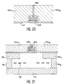
- the first and third vertical walls, 84 and 88 are then selectively etched by selective etching with respect to the material constituting the second wall 84 which is generally made of silica. This etching stops at the upper plane of the layer 100. As shown in FIG. 19, there therefore remain two feet 84 ′ and 88 ′ in silicon at the bottom of the wall 86 in silica.
- pole pieces 104 1 and 104 2 shown in FIG. 20 are then grown by electrolysis. These pieces are separated by the spacer 86.
- the magnetic head obtained is shown in section in FIG. 21. It can be seen that, here again, the magnetoresistive element MR is placed between the pole pieces 104 1 , 104 2 and self-aligned with the non-magnetic spacer. In this variant, the magnetoresistive element MR has a width greater than that of the spacer 86.
Landscapes
- Engineering & Computer Science (AREA)
- Manufacturing & Machinery (AREA)
- Magnetic Heads (AREA)
Applications Claiming Priority (2)
| Application Number | Priority Date | Filing Date | Title |
|---|---|---|---|
| FR9603391 | 1996-03-19 | ||
| FR9603391A FR2746537B1 (fr) | 1996-03-19 | 1996-03-19 | Procede de realisation d'une tete magnetique a element magnetoresistant et tete obtenue par ce procede |
Publications (1)
| Publication Number | Publication Date |
|---|---|
| EP0797189A1 true EP0797189A1 (de) | 1997-09-24 |
Family
ID=9490303
Family Applications (1)
| Application Number | Title | Priority Date | Filing Date |
|---|---|---|---|
| EP97400296A Withdrawn EP0797189A1 (de) | 1996-03-19 | 1997-02-10 | Herstellungsverfahren eines Magnetkopfs mit Magnetowiderstandselement und nach diesem Verfahren erhaltener Kopf |
Country Status (3)
| Country | Link |
|---|---|
| EP (1) | EP0797189A1 (de) |
| JP (1) | JPH1083522A (de) |
| FR (1) | FR2746537B1 (de) |
Citations (3)
| Publication number | Priority date | Publication date | Assignee | Title |
|---|---|---|---|---|
| WO1990011594A1 (fr) * | 1989-03-29 | 1990-10-04 | Commissariat A L'energie Atomique | Tete magnetique de lecture a magnetoresistance pour enregistrement perpendiculaire et procede de realisation d'une telle tete |
| US5208716A (en) * | 1989-03-29 | 1993-05-04 | Commissariat A L'energie Atomique | Magnetoresistant magnetic head for longitudinal recording and process for producing such a head |
| EP0669607A2 (de) * | 1994-02-28 | 1995-08-30 | Read-Rite Corporation | Magnetkopfzusammenbau mit MR-Sensor |
-
1996
- 1996-03-19 FR FR9603391A patent/FR2746537B1/fr not_active Expired - Fee Related
-
1997
- 1997-02-10 EP EP97400296A patent/EP0797189A1/de not_active Withdrawn
- 1997-03-19 JP JP8462497A patent/JPH1083522A/ja not_active Withdrawn
Patent Citations (3)
| Publication number | Priority date | Publication date | Assignee | Title |
|---|---|---|---|---|
| WO1990011594A1 (fr) * | 1989-03-29 | 1990-10-04 | Commissariat A L'energie Atomique | Tete magnetique de lecture a magnetoresistance pour enregistrement perpendiculaire et procede de realisation d'une telle tete |
| US5208716A (en) * | 1989-03-29 | 1993-05-04 | Commissariat A L'energie Atomique | Magnetoresistant magnetic head for longitudinal recording and process for producing such a head |
| EP0669607A2 (de) * | 1994-02-28 | 1995-08-30 | Read-Rite Corporation | Magnetkopfzusammenbau mit MR-Sensor |
Also Published As
| Publication number | Publication date |
|---|---|
| FR2746537A1 (fr) | 1997-09-26 |
| FR2746537B1 (fr) | 1998-07-24 |
| JPH1083522A (ja) | 1998-03-31 |
Similar Documents
| Publication | Publication Date | Title |
|---|---|---|
| EP0153886B1 (de) | Herstellungsverfahren eines Magnetkopfes für senkrechte Aufzeichnung | |
| EP0420755B1 (de) | Herstellungsverfahren eines Magnetaufzeichnungskopfes und nach diesem Verfahren erhaltener Kopf | |
| US7596854B2 (en) | Method of fabrication for read head having shaped read sensor-biasing layer junctions using partial milling | |
| FR2559293A1 (fr) | Nouvelle tete magnetique d'ecriture et de lecture pour enregistrement magnetique et son procede de fabrication | |
| FR2630244A1 (fr) | Dispositif d'ecriture et de lecture sur un support magnetique et son procede de fabrication | |
| FR2726931A1 (fr) | Tete magnetique verticale a bobinage integre et son procede de realisation | |
| EP0880774B1 (de) | Senkrechter magnetkopf mit integrierter spule und herstellungsverfahren | |
| EP0775997A1 (de) | Herstellungsverfahren eines planaren Magnetkopfes und nach diesem Verfahren hergestellter Kopf | |
| JP3529678B2 (ja) | 薄膜磁気ヘッド及びその製造方法 | |
| EP0418127B1 (de) | Herstellungsverfahren von polaren Stücken und der Spalte von Dünnschicht-Magnetköpfen zur Informationsverarbeitungs-, Audio- oder Videoverwendung | |
| WO2006048580A2 (fr) | Dispositif d'enregistrement et/ou de lecture a tetes magnetiques multiples a entrefers azimutes | |
| EP0671724B1 (de) | Vertikaler Magnetkopf und Herstellungsverfahren | |
| EP0670569A1 (de) | Herstellungsverfahren für einen Magnetkopf und mit diesem Verfahen hergestellter senkrechter Kopf | |
| EP0797189A1 (de) | Herstellungsverfahren eines Magnetkopfs mit Magnetowiderstandselement und nach diesem Verfahren erhaltener Kopf | |
| EP0416994B1 (de) | Herstellungsverfahren eines Magnetkopfes mit passend orientierter Achse mit leichter Magnetisierung und nach diesem Verfahren hergestellter Kopf | |
| EP0644528B1 (de) | Aufzeichnungs- und Wiedergabemagnetkopf mit bezüglich Aufzeichnung kompensiertem Magnetowiderstandselement | |
| FR2754905A1 (fr) | Procede de realisation d'un capteur magnetique magnetoresistif et capteur obtenu par ce procede | |
| EP0797188A1 (de) | Magnetkopf mit starker Reluktanz | |
| EP1472680B1 (de) | Integrierter magnetkopf für magnetaufzeichnung und herstellungsverfahren | |
| EP1107236A1 (de) | Flacher Magnetkopf mit magnetoresistivem Element | |
| EP0367880B1 (de) | Herstellungsverfahren eines Aufzeichnungs-/Wiedergabemagnetkopfes | |
| EP0348265A1 (de) | Herstellungsverfahren eines Aufzeichnungs-Wiedergabemagnetkopfes aus einem magnetischen Substrat | |
| EP0811966A1 (de) | Magnetaufzeichnungs- und -wiedergabekopf mit Halbleiter-Feldsensor | |
| FR2744554A1 (fr) | Tete magnetique a element magnetoresistant enterre dans l'entrefer et procede de realisation | |
| US20090103214A1 (en) | Magnetic recording head comprising conical main pole tip and method of manufacturing the same |
Legal Events
| Date | Code | Title | Description |
|---|---|---|---|
| PUAI | Public reference made under article 153(3) epc to a published international application that has entered the european phase |
Free format text: ORIGINAL CODE: 0009012 |
|
| AK | Designated contracting states |
Kind code of ref document: A1 Designated state(s): DE GB IT |
|
| STAA | Information on the status of an ep patent application or granted ep patent |
Free format text: STATUS: THE APPLICATION IS DEEMED TO BE WITHDRAWN |
|
| 18D | Application deemed to be withdrawn |
Effective date: 19980325 |