EP0797189A1 - Process for producing a magnetic head with magnetoresistive element and head obtained by this process - Google Patents
Process for producing a magnetic head with magnetoresistive element and head obtained by this process Download PDFInfo
- Publication number
- EP0797189A1 EP0797189A1 EP97400296A EP97400296A EP0797189A1 EP 0797189 A1 EP0797189 A1 EP 0797189A1 EP 97400296 A EP97400296 A EP 97400296A EP 97400296 A EP97400296 A EP 97400296A EP 0797189 A1 EP0797189 A1 EP 0797189A1
- Authority
- EP
- European Patent Office
- Prior art keywords
- layer
- magnetic
- wall
- insulating
- stack
- Prior art date
- Legal status (The legal status is an assumption and is not a legal conclusion. Google has not performed a legal analysis and makes no representation as to the accuracy of the status listed.)
- Withdrawn
Links
Images


Classifications
-
- G—PHYSICS
- G11—INFORMATION STORAGE
- G11B—INFORMATION STORAGE BASED ON RELATIVE MOVEMENT BETWEEN RECORD CARRIER AND TRANSDUCER
- G11B5/00—Recording by magnetisation or demagnetisation of a record carrier; Reproducing by magnetic means; Record carriers therefor
- G11B5/127—Structure or manufacture of heads, e.g. inductive
- G11B5/33—Structure or manufacture of flux-sensitive heads, i.e. for reproduction only; Combination of such heads with means for recording or erasing only
- G11B5/39—Structure or manufacture of flux-sensitive heads, i.e. for reproduction only; Combination of such heads with means for recording or erasing only using magneto-resistive devices or effects
- G11B5/3903—Structure or manufacture of flux-sensitive heads, i.e. for reproduction only; Combination of such heads with means for recording or erasing only using magneto-resistive devices or effects using magnetic thin film layers or their effects, the films being part of integrated structures
-
- G—PHYSICS
- G11—INFORMATION STORAGE
- G11B—INFORMATION STORAGE BASED ON RELATIVE MOVEMENT BETWEEN RECORD CARRIER AND TRANSDUCER
- G11B5/00—Recording by magnetisation or demagnetisation of a record carrier; Reproducing by magnetic means; Record carriers therefor
- G11B5/127—Structure or manufacture of heads, e.g. inductive
- G11B5/31—Structure or manufacture of heads, e.g. inductive using thin films
- G11B5/3163—Fabrication methods or processes specially adapted for a particular head structure, e.g. using base layers for electroplating, using functional layers for masking, using energy or particle beams for shaping the structure or modifying the properties of the basic layers
Definitions
- the subject of the present invention is a method for producing a magnetic head with a magnetoresistive element and a magnetic head obtained by this method.
- Magnetic heads are known which are produced in a so-called horizontal thin film technique. Such heads are described in document FR-A-2,645,314 (or in its American correspondent US-A-5,208,716). A head of this kind is shown in Figure 1 attached.
- a horizontal head comprising a semiconductor substrate 10, for example made of silicon, in which a box 12 has been etched.
- a lower magnetic layer 14 has been formed electrolytically and has been extended by two pillars 16 1 , 16 2 .
- a conductive winding 18 surrounds the pillars.
- This coil is embedded in an insulating layer 20.
- the magnetic circuit is completed by an upper magnetic part comprising two pole pieces 22 1 , 22 2 separated by a non-magnetic spacer 24.
- a magnetoresistive element MR by example in iron-nickel, is arranged under the non-magnetic spacer 24, in the insulator 20.
- the head moves in front of a magnetic support 30 where the information to be read or written is recorded.
- the current flowing in the winding 18 creates a magnetic field and, consequently, an induction in the magnetic circuit.
- the field lines which open out around the spacer induce a magnetization in the support 30.
- magnetic information recorded in the support 30 produces a magnetic reading field and, consequently, an induction in the magnetic circuit.
- This induction closes, in part, through the magnetoresistive element MR.
- a variant of these heads consists in adding between the pillars and the pole pieces two magnetic pieces constituting flux concentrators. Such heads are described in FR-A-2 712 420 and in FR-A-2 709 855.
- the object of the invention is precisely to solve this double technical problem.
- the invention proposes a method of producing a magnetic head which makes it possible to place the magnetoresistive element in the air gap itself, that is to say between the two pole pieces and no longer under the level of these. Furthermore, the method allows automatic alignment of the magnetoresistive element with respect to the air gap.
- a wall is formed which comprises only a non-magnetic wall.
- the width of the magnetoresistive element remaining after etching is then equal to that of the non-magnetic spacer.
- a wall is formed which comprises two vertical walls of insulating material framing a vertical wall of non-magnetic material, and, after having etched the stack of layers using these three walls as a mask, the two vertical insulating walls on either side of the non-magnetic wall to leave only the non-magnetic wall. The width of the magnetoresistant element remaining is then greater than that of the non-magnetic spacer.
- the present invention also relates to a magnetic head obtained by this process.
- This head is of the type which includes a magnetic circuit with two pole pieces separated by a non-magnetic spacer and a magnetoresistive element.
- the head of the invention is characterized in that the magnetoresistive element is located between the two pole pieces and is self-aligned with the non-magnetic spacer.
- This sub-assembly comprises a lower magnetic part 14, two magnetic pillars 16 1 , 16 2 and two concentrators 32 1 , 32 2 .
- a conductive winding 18 surrounds the pillars 16 1 , 16 2 .
- the assembly is embedded in an insulator 20.
- This sub-assembly has a flat upper surface 34, on which different layers will be deposited and etched according to the invention.
- the first layer 41 of conductive material, must have good adhesion, and must be selectively etched with respect to an insulator such as silica. Many materials can be used for this purpose, such as tungsten, chromium, titanium, etc. In the following, we will assume that we have chosen tungsten.
- the thickness of this layer can be a fraction of a micrometer.
- the material of the second layer 42 must be able to be etched selectively with respect to the metal sublayer 41. It can be, for example, silica SiO 2 . It is on this insulating layer, for example made of silica, that the layer which will constitute the magnetoresistive element is deposited. This layer can be of any material magnetoresistive. They may in particular be multilayers.
- the second insulating layer 44 may be identical to the first, 42, and the second metal layer 45 identical to the first, 41, that is to say respectively of silica and tungsten, for example.
- an insulating layer 50 for example of resin, a few micrometers thick, is deposited.
- a step 52 is engraved with a riser 54, as illustrated in FIG. 5.
- a thin layer of insulator 56 is then deposited, for example by LPCVD ("Low Pressure Chemical Vapor Deposition"). This layer is deposited on horizontal surfaces, but also on the vertical riser. The thickness of this layer must correspond to the length of the future air gap, (that is to say to its dimension taken in the direction of movement of the recording medium).
- LPCVD Low Pressure Chemical Vapor Deposition
- the layer 56 is etched, to make the horizontal parts disappear but leave a vertical wall 60 on the riser, as illustrated in FIG. 7.
- the upper metal layer 45 serves stop layer.
- the resin step 52 is then removed and a vertical wall 60 is obtained as illustrated in FIG. 8.
- the stack of layers 40 is then attacked, with the exception of the first metallic layer 41.
- the second metal layer 45 is thus etched, which is made of tungsten for example; then, by changing the etching method, the second insulating layer 44 is etched, which is for example made of SiO 2 ; the etching method is further changed to etch the layer of magnetoresistive material 43; the etching specific to the insulating material is resumed to etch the first insulating layer 42, and one stops on the first metallic layer 41, which is for example made of tungsten.
- FIG. 9 We then obtain the assembly illustrated in FIG. 9 where we see under the wall 60, an engraved stack 62 comprising a first insulating tape 64, a magnetoresistive tape MR, a second insulating tape 66 and a metal tape 68. of its mode of obtaining by etching the wall 60 being taken as a mask, the assembly 62, therefore the element MR, is automatically aligned with respect to the wall.
- a layer of insulation (resin, silica, etc.) is then deposited with a thickness greater than the thickness of the stack 62, and this layer is etched , for example in oxygen plasma. There then remain, on the flanks of the engraved stack, layers 70 1 , 70 2 shown in FIG. 10.
- the two pole pieces 72 1 , 72 2 can be made of iron-nickel for example.
- the magnetoresistive element MR which is placed by construction, above the first metallic layer 41, is found situated above the lower level of the pole pieces, in other words between the pole pieces and no longer under those -this, as in the prior art. This arrangement is very favorable to the operation of reading the recording, since the magnetic field lines will borrow the magnetoresistive element more effectively.
- the width of the magnetoresistive element is less than or equal to the dimension of the non-magnetic gap counted in the direction of movement of the recording medium (dimension which is generally names "length").
- dimension which is generally names "length” dimension which is generally names "length"
- the invention is not limited to this particular case and also encompasses the case where the width of the magnetoresistive element is greater than the length of the air gap. This second mode of implementation is illustrated in FIGS. 13 to 21.
- a material meeting these requirements is polycrystalline silicon. This material can be deposited either by sputtering or by LPCVD with good market coverage.
- the layer 82 which can therefore be made of polycrystalline silicon, has a thickness on the flank of between approximately 0.1 microns and a few microns.
- This layer 82 is then etched vertically by stopping on the second metal layer 45 and a first vertical wall 84 is obtained as shown in FIG. 14.
- an insulating layer 86 for example of silica SiO 2 , whose thickness along the vertical wall is equal to the length of the future air gap.
- the layer 86 is etched vertically, stopping again on the second metal layer 45. This then gives a second vertical wall 86 pressed against the side of the first, 84.
- a layer of a material identical to that of layer 82 is deposited again, therefore for example in polycrystalline silicon and, after vertical etching as in FIG. 14, a third wall is obtained vertical 88 in silicon.
- the three walls are shown in Figure 16.
- the second wall 86 constitutes the future non-magnetic spacer.
- this set of three vertical walls 84, 86, 88 is then used as a mask for etching the initial stack 40 of metallic, insulating and magnetoresistive layers by taking the first metallic layer 41 as layer d 'stop.
- the arrangement illustrated in FIG. 17 is then obtained, where the engraved stack bears the reference 90.
- This engraved stack is composed of a first insulating tape 92, a magnetoresistive tape MR and a second magnetoresistant tape 96.
- This stack has naturally a width equal to that of all three vertical walls 84, 86, 88 and it is therefore wider than the future spacer 86.
- the following operation consists in depositing an insulating layer 100, for example made of resin or silica, with a thickness greater than that of the engraved assembly (FIG. 18).
- the first and third vertical walls, 84 and 88 are then selectively etched by selective etching with respect to the material constituting the second wall 84 which is generally made of silica. This etching stops at the upper plane of the layer 100. As shown in FIG. 19, there therefore remain two feet 84 ′ and 88 ′ in silicon at the bottom of the wall 86 in silica.
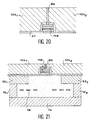
- pole pieces 104 1 and 104 2 shown in FIG. 20 are then grown by electrolysis. These pieces are separated by the spacer 86.
- the magnetic head obtained is shown in section in FIG. 21. It can be seen that, here again, the magnetoresistive element MR is placed between the pole pieces 104 1 , 104 2 and self-aligned with the non-magnetic spacer. In this variant, the magnetoresistive element MR has a width greater than that of the spacer 86.
Abstract
Description
La présente invention a pour objet un procédé de réalisation d'une tête magnétique à élément magnétorésistant et une tête magnétique obtenue par ce procédé.The subject of the present invention is a method for producing a magnetic head with a magnetoresistive element and a magnetic head obtained by this method.
Elle trouve une application dans l'enregistrement magnétique.It finds application in magnetic recording.
On connaît des têtes magnétiques réalisées dans une technique dite horizontale à couches minces. De telles têtes sont décrites dans le document FR-A-2 645 314 (ou dans son correspondant américain US-A-5,208,716). Une tête de ce genre est présentée sur la figure 1 annexée.Magnetic heads are known which are produced in a so-called horizontal thin film technique. Such heads are described in document FR-A-2,645,314 (or in its American correspondent US-A-5,208,716). A head of this kind is shown in Figure 1 attached.
Sur cette figure, on voit, en coupe, une tête horizontale comprenant un substrat semiconducteur 10, par exemple en silicium, dans lequel a été gravé un caisson 12. Dans ce caisson, une couche magnétique inférieure 14 a été formée électrolytiquement et a été prolongée par deux piliers 161, 162. Un bobinage conducteur 18 entoure les piliers. Ce bobinage est noyé dans une couche isolante 20. Le circuit magnétique se complète par une pièce magnétique supérieure comprenant deux pièces polaires 221, 222 séparées par un espaceur amagnétique 24. Un élément magnétorésistant MR, par exemple en fer-nickel, est disposé sous l'espaceur amagnétique 24, dans l'isolant 20. La tête se déplace devant un support magnétique 30 où sont enregistrées les informations à lire ou à écrire.In this figure, we can see, in section, a horizontal head comprising a
Le fonctionnement d'une telle tête est schématiquement le suivant.The operation of such a head is schematically as follows.
A l'écriture, le courant circulant dans le bobinage 18 crée un champ magnétique et, par conséquent, une induction dans le circuit magnétique. Les lignes de champ qui s'épanouissent autour de l'espaceur induisent une aimantation dans le support 30.When writing, the current flowing in the winding 18 creates a magnetic field and, consequently, an induction in the magnetic circuit. The field lines which open out around the spacer induce a magnetization in the
A la lecture, une information magnétique enregistrée dans le support 30 produit un champ magnétique de lecture et, par conséquent, une induction dans le circuit magnétique. Cette induction se referme, en partie, à travers l'élément magnétorésistant MR. Il en résulte une rotation d'aimantation dans cet élément, qui va provoquer une variation de sa résistance. En faisant circuler un courant dans cet élément, on pourra mesurer sa variation de résistance et, en conséquence, retrouver l'information lue.On reading, magnetic information recorded in the
Une variante de ces têtes consiste à ajouter entre les piliers et les pièces polaires deux pièces magnétiques constituant des concentrateurs de flux. De telles têtes sont décrites dans FR-A-2 712 420 et dans FR-A-2 709 855.A variant of these heads consists in adding between the pillars and the pole pieces two magnetic pieces constituting flux concentrators. Such heads are described in FR-A-2 712 420 and in FR-A-2 709 855.
Bien que donnant satisfaction à certains égards, de telles têtes présentent un inconvénient lié à la position de l'élément magnétorésistant par rapport à l'entrefer. Cet élément est, en effet, situé sous le niveau-général des pièces polaires. Il en résulte une faible efficacité en lecture, car une partie seulement du flux magnétique de lecture se referme par l'élément magnétorésistant. Par ailleurs, dans bien des cas, et notamment dans celui des magnétorésistances multicouches à effet magnétorésistant géant (dites encore à vannes de spin ou "spin-valves" en terminologie anglosaxonne). Il est nécessaire que la largeur de l'élément soit le plus faible possible pour réduire le champ démagnétisant. Mais se pose alors le problème de l'alignement correct de cet élément par rapport à l'entrefer.Although satisfactory in certain respects, such heads have a drawback linked to the position of the magnetoresistive element relative to the air gap. This element is, in fact, located under the general level of the pole pieces. This results in a low reading efficiency, because only part of the magnetic reading flow closes by the magnetoresistive element. Furthermore, in many cases, and in particular in that of multilayer magnetoresistors with giant magnetoresistive effect (also called spin valves or "spin-valves" in English terminology). It is necessary that the width of the element is as small as possible to reduce the demagnetizing field. But then the problem arises of the correct alignment of this element with respect to the air gap.
Le but de l'invention est justement de résoudre ce double problème technique.The object of the invention is precisely to solve this double technical problem.
A cette fin, l'invention propose un procédé de réalisation d'une tête magnétique qui permet de placer l'élément magnétorésistant dans l'entrefer lui-même, c'est-à-dire entre les deux pièces polaires et non plus sous le niveau de celles-ci. Par ailleurs, le procédé permet un alignement automatique de l'élément magnétorésistant par rapport à l'entrefer.To this end, the invention proposes a method of producing a magnetic head which makes it possible to place the magnetoresistive element in the air gap itself, that is to say between the two pole pieces and no longer under the level of these. Furthermore, the method allows automatic alignment of the magnetoresistive element with respect to the air gap.
Cet objectif est atteint, selon l'invention, de la manière suivante. On commence par réaliser un sous-ensemble classique comprenant une partie de circuit magnétique. Le procédé de l'invention se poursuit alors par les opérations suivantes :
- on forme sur ce sous-ensemble un empilement de couches en déposant successivement une première couche métallique, une première couche isolante, une couche magnétorésistante, une seconde couche isolante et enfin une seconde couche métallique,
- on forme sur cet empilement un mur isolant comprenant au moins un espaceur amagnétique,
- en prenant ce mur comme masque, on grave l'empilement de couches jusqu'à atteindre la première couche métallique prise comme couche d'arrêt, ce qui laisse subsister, sur la première couche métallique et sous le mur, un empilement gravé comprenant un élément magnétorésistant intercalé entre un premier et un second rubans isolants,
- on prend la première couche métallique subsistant comme électrode et l'on forme, par croissance électrolytique, une pièce magnétique supérieure composée de deux pièces polaires séparées par l'espaceur amagnétique, l'élément magnétorésistant se trouvant ainsi autoaligné avec ledit espaceur et inséré entre les deux pièces polaires.
- a stack of layers is formed on this sub-assembly by successively depositing a first metallic layer, a first insulating layer, a magnetoresistive layer, a second insulating layer and finally a second metallic layer,
- an insulating wall is formed on this stack comprising at least one non-magnetic spacer,
- by taking this wall as a mask, the stack of layers is etched until reaching the first metallic layer taken as a stop layer, which leaves an etched stack comprising an element on the first metallic layer and under the wall. magnetoresistant inserted between a first and a second insulating tape,
- the first remaining metallic layer is taken as the electrode and an upper magnetic part composed of two pole pieces separated by the non-magnetic spacer is formed by electrolytic growth, the magnetoresistive element thus being self-aligned with said spacer and inserted between the two pole pieces.
Dans un premier mode de mise en oeuvre de ce procédé, on forme un mur qui ne comprend qu'une paroi amagnétique. La largeur de l'élément magnétorésistant subsistant après gravure est alors égale à celle de l'espaceur amagnétique.In a first embodiment of this method, a wall is formed which comprises only a non-magnetic wall. The width of the magnetoresistive element remaining after etching is then equal to that of the non-magnetic spacer.
Dans un second mode de mise en oeuvre, on forme un mur qui comprend deux parois verticales en matériau isolant encadrant une paroi verticale en matériau amagnétique, et, après avoir gravé l'empilement de couches en prenant ces trois parois comme masque, on grave les deux parois verticales isolantes de part et d'autre de la paroi amagnétique pour ne laisser subsister que la paroi amagnétique. La largeur de l'élément magnétorésistant subsistant est alors supérieure à celle de l'espaceur amagnétique.In a second embodiment, a wall is formed which comprises two vertical walls of insulating material framing a vertical wall of non-magnetic material, and, after having etched the stack of layers using these three walls as a mask, the two vertical insulating walls on either side of the non-magnetic wall to leave only the non-magnetic wall. The width of the magnetoresistant element remaining is then greater than that of the non-magnetic spacer.
La présente invention a également pour objet une tête magnétique obtenue par ce procédé. Cette tête est du genre de celles qui comprennent un circuit magnétique avec deux pièces polaires séparées par un espaceur amagnétique et un élément magnétorésistant. La tête de l'invention est caractérisée par le fait que l'élément magnétorésistant est situé entre les deux pièces polaires et est autoaligné avec l'espaceur amagnétique.The present invention also relates to a magnetic head obtained by this process. This head is of the type which includes a magnetic circuit with two pole pieces separated by a non-magnetic spacer and a magnetoresistive element. The head of the invention is characterized in that the magnetoresistive element is located between the two pole pieces and is self-aligned with the non-magnetic spacer.
- la figure 1, déjà décrite, montre une tête magnétique en couches minces connue dont l'élément magnétorésistant est situé sous les pièces polaires ;Figure 1, already described, shows a known thin film magnetic head whose magnetoresistive element is located under the pole pieces;
- la figure 2 illustre une étape préliminaire du procédé de l'invention ;FIG. 2 illustrates a preliminary step of the method of the invention;
- la figure 3 montre un empilement de cinq couches, dont une couche en matériau magnétorésistant ;Figure 3 shows a stack of five layers, including a layer of magnetoresistive material;
- la figure 4 illustre une opération de dépôt d'une couche de résine ;FIG. 4 illustrates an operation for depositing a layer of resin;
- la figure 5 illustre une étape de photolithographie ;FIG. 5 illustrates a photolithography step;
- la figure 6 illustre une étape de dépôt d'un film isolant ;FIG. 6 illustrates a step of depositing an insulating film;
- la figure 7 illustre une opération de gravure ;FIG. 7 illustrates an engraving operation;
- la figure 8 montre l'espaceur amagnétique finalement obtenu ;FIG. 8 shows the non-magnetic spacer finally obtained;
- la figure 9 illustre une opération de gravure de l'empilement ;FIG. 9 illustrates an operation for engraving the stack;
- la figure 10 illustre l'opération de dépôt d'une couche isolante sur la tranche de l'empilement gravé ;FIG. 10 illustrates the operation of depositing an insulating layer on the edge of the etched stack;
- la figure 11 illustre l'opération de croissance électrolytique de la pièce magnétique supérieure ;FIG. 11 illustrates the electrolytic growth operation of the upper magnetic part;
- la figure 12 montre, en coupe, la tête magnétique complète dans un premier mode de réalisation ;Figure 12 shows, in section, the complete magnetic head in a first embodiment;
- la figure 13 illustre une étape de dépôt de silicium sur une marche de résine ;FIG. 13 illustrates a step of depositing silicon on a resin step;
- la figure 14 Illustre une opération de gravure verticale ;Figure 14 illustrates a vertical engraving operation;
- la figure 15 montre le dépôt d'une couche de matériau isolant amagnétique ;FIG. 15 shows the deposition of a layer of non-magnetic insulating material;
- la figure 16 montre un mur composé d'un espaceur amagnétique encadré par deux parois de silicium ;FIG. 16 shows a wall composed of a non-magnetic spacer surrounded by two silicon walls;
- la figure 17 illustre l'opération de gravure de l'empilement en prenant le mur comme masque ;FIG. 17 illustrates the engraving operation of the stack using the wall as a mask;
- la figure 18 montre le dépôt d'une couche de résine ;Figure 18 shows the deposition of a resin layer;
- la figure 19 montre l'espaceur amagnétique et l'empilement gravé dont les flancs ont été recouverts d'isolant ;FIG. 19 shows the non-magnetic spacer and the engraved stack, the sides of which have been covered with insulation;
- la figure 20 illustre l'opération de croissance électrolytique de la couche magnétique supérieure ;FIG. 20 illustrates the operation of electrolytic growth of the upper magnetic layer;
- la figure 21 montre, en coupe, la tête magnétique finalement obtenue selon un deuxième mode de réalisation.FIG. 21 shows, in section, the magnetic head finally obtained according to a second embodiment.
Avant de mettre en oeuvre les opérations spécifiques à l'invention, on réalise un sous-ensemble tel que celui qui est représenté sur la figure 2. Ce sous-ensemble comprend une pièce magnétique inférieure 14, deux piliers magnétiques 161, 162 et deux concentrateurs 321, 322. Un bobinage conducteur 18 entoure les piliers 161, 162. L'ensemble est noyé dans un isolant 20. Ce sous-ensemble présente une surface supérieure plane 34, sur laquelle différentes couches vont être déposées et gravées selon l'invention.Before implementing the operations specific to the invention, a sub-assembly such as that shown in FIG. 2 is produced. This sub-assembly comprises a lower
Comme illustré sur la figure 3, on commence par déposer sur la surface 34 un empilement 40 de couches comprenant successivement une première couche métallique 41, une première couche isolante 42, une couche magnétorésistante 43, une seconde couche isolante 44 et enfin une seconde couche métallique 45.As illustrated in FIG. 3, one begins by depositing on the surface 34 a
La première couche 41, en matériau conducteur, doit présenter une bonne adhérence, et doit se graver sélectivement par rapport à un isolant comme la silice. De nombreux matériaux peuvent être utilisés à cette fin, comme le tungstène, le chrome, le titane, etc... Dans la suite, on supposera que l'on a choisi le tungstène. L'épaisseur de cette couche peut être une fraction de micromètre. Le matériau de la seconde couche 42 doit pouvoir être gravé sélectivement par rapport à la sous-couche métallique 41. Il peut s'agir, par exemple, de la silice SiO2. C'est sur cette couche isolante, par exemple en silice, qu'est déposée la couche qui va constituer l'élément magnétorésistant. Cette couche peut être en tout matériau magnétorésistif. Il peut s'agir notamment de multicouches.The
La seconde couche isolante 44 peut être identique à la première, 42, et la seconde couche métallique 45 identique à la première, 41, c'est-à-dire respectivement en silice et en tungstène, par exemple.The second insulating
Sur cet empilement 40, et comme représenté sur la figure 4, on dépose une couche isolante 50, par exemple en résine, de quelques micromètres d'épaisseur. Par une opération de photolithographie, on grave une marche 52 avec une contremarche 54, comme illustré sur la figure 5.On this
Sur l'ensemble et comme représenté sur la figure 6, on dépose ensuite une couche fine d'isolant 56, par exemple par LPCVD ("Low Pressure Chemical Vapor Deposition"). Cette couche se dépose sur les surfaces horizontales, mais également sur la contremarche verticale. L'épaisseur de cette couche doit correspondre à la longueur du futur entrefer, (c'est-à-dire à sa dimension prise dans le sens du déplacement du support d'enregistrement).On the assembly and as shown in FIG. 6, a thin layer of
Par gravure ionique réactive (RIE), on grave la couche 56, pour faire disparaître les parties horizontales mais laisser subsister une paroi verticale 60 sur la contremarche, comme illustré sur la figure 7. Dans cette opération de gravure, la couche métallique supérieure 45 sert de couche d'arrêt.By reactive ion etching (RIE), the
On enlève ensuite la marche de résine 52 et l'on obtient un mur vertical 60 tel qu'illustré sur la figure 8.The
Par gravure ionique (réactive ou non réactive, selon les couches à graver), on attaque ensuite l'empilement de couches 40, à l'exception de la première couche métallique 41. C'est ce qui est illustré sur la figure 9 où le pied de l'espaceur a été agrandi pour plus de clarté. On grave ainsi la deuxième couche métallique 45, qui est en tungstène par exemple ; puis, en changeant de méthode de gravure, on grave la seconde couche isolante 44, qui est par exemple en SiO2 ; on change encore de méthode de gravure pour graver la couche de matériau magnétorésistant 43 ; on reprend la gravure propre au matériau isolant pour graver la première couche isolante 42, et l'on s'arrête sur la première couche métallique 41, qui est par exemple en tungstène. On obtient alors l'ensemble illustré sur la figure 9 où l'on voit sous le mur 60, un empilement gravé 62 comprenant un premier ruban isolant 64, un ruban magnétorésistant MR, un second ruban isolant 66 et un ruban métallique 68. Du fait de son mode d'obtention par gravure le mur 60 étant pris comme masque, l'ensemble 62, donc l'élément MR, est automatiquement aligné par rapport au mur.By ion etching (reactive or non-reactive, depending on the layers to be etched), the stack of
Pour isoler les flancs de l'empilement gravé 62, on dépose ensuite une couche d'isolant (résine, silice, etc...) d'épaisseur supérieure à l'épaisseur de l'empilement 62, et l'on grave cette couche, par exemple en plasma d'oxygène. Il reste alors, sur les flancs de l'empilement gravé, des couches 701, 702 représentées sur la figure 10.To isolate the sides of the engraved
Prenant ensuite la première couche métallique 41 comme électrode, on fait croître par électrolyse une couche magnétique supérieure formée de deux pièces polaires 721, 722, qui se forment de part et d'autre du mur 60, lequel va donc constituer l'espaceur amagnétique. C'est ce qui est représenté sur la figure 12. Les deux pièces polaires 721, 722 peuvent être en fer-nickel par exemple.Then taking the first
On observera attentivement que l'élément magnétorésistant MR, qui est placé par construction, au-dessus de la première couche métallique 41, se retrouve situé au-dessus du niveau inférieur des pièces polaires, autrement dit entre les pièces polaires et non plus sous celles-ci, comme dans l'art antérieur. Cette disposition est très favorable à l'opération de la lecture de l'enregistrement, car les lignes de champ magnétique vont emprunter l'élément magnétorésistant de manière plus efficace.It will be observed carefully that the magnetoresistive element MR, which is placed by construction, above the first
Le tête magnétique finalement obtenue est représentée sur la figure 12, où les références numériques déjà utilisées désignent les mêmes éléments.The finally obtained magnetic head is shown in FIG. 12, where the numerical references already used designate the same elements.
Dans le mode de mise en oeuvre qui vient d'être décrit, la largeur de l'élément magnétorésistant est inférieure ou égale à la dimension de l'entrefer amagnétique comptée dans le sens de déplacement du support d'enregistrement (dimension que l'on nomme généralement "longueur"). Mais l'invention ne se limite à ce cas particulier et englobe aussi le cas où la largeur de l'élément magnétorésistant est supérieure à la longueur de l'entrefer. Ce second mode de mise en oeuvre est illustré sur les figures 13 à 21.In the embodiment which has just been described, the width of the magnetoresistive element is less than or equal to the dimension of the non-magnetic gap counted in the direction of movement of the recording medium (dimension which is generally names "length"). However, the invention is not limited to this particular case and also encompasses the case where the width of the magnetoresistive element is greater than the length of the air gap. This second mode of implementation is illustrated in FIGS. 13 to 21.
Sur la figure 13 on voit un sous-ensemble analogue à celui de la figure 6, avec une marche 80 et une couche 82 en un matériau devant présenter plusieurs propriétés particulières, à savoir qu'il doit pouvoir être gravé :
- par les techniques permettant d'obtenir une gravure verticale, c'est-à-dire généralement la gravure ionique réactive,
- sélectivement par rapport à l'isolant choisi pour constituer l'espaceur,
- sélectivement par rapport à la seconde couche conductrice supérieure (par exemple du tungstène).
- by the techniques making it possible to obtain vertical etching, that is to say generally reactive ion etching,
- selectively with respect to the insulation chosen to constitute the spacer,
- selectively with respect to the second upper conductive layer (for example tungsten).
Un matériau répondant à ces exigences est le silicium polycristallin. Ce matériau peut être déposé soit par pulvérisation cathodique, soit par LPCVD avec une bonne couverture de marche.A material meeting these requirements is polycrystalline silicon. This material can be deposited either by sputtering or by LPCVD with good market coverage.
La couche 82, qui peut donc être en silicium polycristallin, présente une épaisseur sur le flanc comprise entre environ 0,1 micron et quelques microns.The
On grave ensuite verticalement cette couche 82 en s'arrêtant sur la seconde couche métallique 45 et l'on obtient une première paroi verticale 84 comme représentée sur la figure 14.This
On dépose alors sur l'ensemble, comme représenté sur la figure 15, une couche 86 d'isolant, par exemple en silice SiO2, dont l'épaisseur le long de la paroi verticale est égale à la longueur du futur entrefer.Then deposited on the assembly, as shown in Figure 15, an insulating
On grave verticalement la couche 86 en s'arrêtant encore sur la seconde couche métallique 45. On obtient alors une deuxième paroi verticale 86 plaquée sur le flanc de la première, 84.The
On dépose à nouveau une couche d'un matériau identique à celui de la couche 82, donc par exemple en silicium polycristallin et, après gravure verticale comme pour la figure 14, on obtient une troisième paroi verticale 88 en silicium. Les trois parois sont représentées sur la figure 16. La deuxième paroi 86 constitue le futur espaceur amagnétique.A layer of a material identical to that of
De la même manière que dans la première variante, on utilise ensuite cet ensemble de trois parois verticales 84, 86, 88 comme masque pour graver l'empilement initial 40 de couches métalliques, isolantes et magnétorésistante en prenant la première couche métallique 41 comme couche d'arrêt. On obtient alors la disposition illustrée sur la figure 17, où l'empilement gravé porte la référence 90. Cet empilement gravé est composé d'un premier ruban isolant 92, un ruban magnétorésistant MR et d'un second ruban magnétorésistant 96. Cet empilement présente naturellement une largeur égale à celle de l'ensemble des trois parois verticales 84, 86, 88 et il est donc plus large que le futur espaceur 86.In the same way as in the first variant, this set of three
L'opération suivante consiste à déposer une couche isolante 100, par exemple en résine ou en silice, avec une épaisseur supérieure à celle de l'ensemble gravé (figure 18).The following operation consists in depositing an insulating
On grave ensuite sélectivement la première et la troisième parois verticales, 84 et 88, toutes deux en silicium polycristallin, par une gravure sélective par rapport au matériau constituant la deuxième paroi 84 qui est en général en silice. Cette gravure s'arrête au plan supérieur de la couche 100. Comme représenté sur la figure 19, il subsiste donc deux pieds 84' et 88' en silicium à la partie inférieure du mur 86 en silice.The first and third vertical walls, 84 and 88, both made of polycrystalline silicon, are then selectively etched by selective etching with respect to the material constituting the
En gravant la couche 100 en prenant la seconde couche métallique 41, comme couche d'arrêt il reste deux parois isolantes 1021, 1022 représentée sur la figure 19.By etching the
En prenant la couche métallique 41 comme électrode, on fait croître ensuite par électrolyse deux pièces polaires 1041 et 1042 représentées sur la figure 20. Ces pièces se trouvent séparées par l'espaceur 86.By taking the
La tête magnétique obtenue est représentée en coupe sur la figure 21. On voit que, là encore, l'élément magnétorésistant MR est disposé entre les pièces polaires 1041, 1042 et autoaligné avec l'espaceur amagnétique. Dans cette variante, l'élément magnétorésistant MR a une largeur supérieure à celle de l'espaceur 86.The magnetic head obtained is shown in section in FIG. 21. It can be seen that, here again, the magnetoresistive element MR is placed between the pole pieces 104 1 , 104 2 and self-aligned with the non-magnetic spacer. In this variant, the magnetoresistive element MR has a width greater than that of the
Claims (14)
ce procédé étant caractérisé par le fait qu'il se poursuit par les opérations suivantes :
this process being characterized by the fact that it continues with the following operations:
Applications Claiming Priority (2)
| Application Number | Priority Date | Filing Date | Title |
|---|---|---|---|
| FR9603391A FR2746537B1 (en) | 1996-03-19 | 1996-03-19 | METHOD FOR PRODUCING A MAGNETIC HEAD WITH A MAGNETORESISTENT ELEMENT AND HEAD OBTAINED BY THIS METHOD |
| FR9603391 | 1996-03-19 |
Publications (1)
| Publication Number | Publication Date |
|---|---|
| EP0797189A1 true EP0797189A1 (en) | 1997-09-24 |
Family
ID=9490303
Family Applications (1)
| Application Number | Title | Priority Date | Filing Date |
|---|---|---|---|
| EP97400296A Withdrawn EP0797189A1 (en) | 1996-03-19 | 1997-02-10 | Process for producing a magnetic head with magnetoresistive element and head obtained by this process |
Country Status (3)
| Country | Link |
|---|---|
| EP (1) | EP0797189A1 (en) |
| JP (1) | JPH1083522A (en) |
| FR (1) | FR2746537B1 (en) |
Citations (3)
| Publication number | Priority date | Publication date | Assignee | Title |
|---|---|---|---|---|
| WO1990011594A1 (en) * | 1989-03-29 | 1990-10-04 | Commissariat A L'energie Atomique | Magnetic reading head with magnetoresistance for perpendicular recording and method for making such head |
| US5208716A (en) * | 1989-03-29 | 1993-05-04 | Commissariat A L'energie Atomique | Magnetoresistant magnetic head for longitudinal recording and process for producing such a head |
| EP0669607A2 (en) * | 1994-02-28 | 1995-08-30 | Read-Rite Corporation | Magnetic head assembly with MR sensor |
-
1996
- 1996-03-19 FR FR9603391A patent/FR2746537B1/en not_active Expired - Fee Related
-
1997
- 1997-02-10 EP EP97400296A patent/EP0797189A1/en not_active Withdrawn
- 1997-03-19 JP JP8462497A patent/JPH1083522A/en not_active Withdrawn
Patent Citations (3)
| Publication number | Priority date | Publication date | Assignee | Title |
|---|---|---|---|---|
| WO1990011594A1 (en) * | 1989-03-29 | 1990-10-04 | Commissariat A L'energie Atomique | Magnetic reading head with magnetoresistance for perpendicular recording and method for making such head |
| US5208716A (en) * | 1989-03-29 | 1993-05-04 | Commissariat A L'energie Atomique | Magnetoresistant magnetic head for longitudinal recording and process for producing such a head |
| EP0669607A2 (en) * | 1994-02-28 | 1995-08-30 | Read-Rite Corporation | Magnetic head assembly with MR sensor |
Also Published As
| Publication number | Publication date |
|---|---|
| FR2746537A1 (en) | 1997-09-26 |
| JPH1083522A (en) | 1998-03-31 |
| FR2746537B1 (en) | 1998-07-24 |
Similar Documents
| Publication | Publication Date | Title |
|---|---|---|
| EP0153886B1 (en) | Process for the fabrication of a perpendicular recording magnetic head | |
| EP0420755B1 (en) | Process for producing a magnetic recording head and head obtained by this process | |
| US7596854B2 (en) | Method of fabrication for read head having shaped read sensor-biasing layer junctions using partial milling | |
| FR2559293A1 (en) | NOVEL MAGNETIC WRITE AND READ HEAD FOR MAGNETIC RECORDING AND METHOD FOR MANUFACTURING THE SAME | |
| FR2630244A1 (en) | DEVICE FOR WRITING AND READING ON A MAGNETIC MEDIUM AND METHOD FOR MANUFACTURING THE SAME | |
| FR2726931A1 (en) | VERTICAL MAGNETIC HEAD WITH INTEGRATED WINDING AND METHOD FOR PRODUCING THE SAME | |
| EP0880774B1 (en) | Vertical magnetic head with integrated coiling and process for making same | |
| EP0775997A1 (en) | Process for producing a planar magnetic head and head obtained by this process | |
| JP3529678B2 (en) | Thin film magnetic head and method of manufacturing the same | |
| EP0418127B1 (en) | Process for producing pole pieces and gap of thin layer magnetic heads for information processing, audio or video | |
| WO2006048580A2 (en) | Recording and/or playback device comprising multiple magnetic heads with azimuth gaps | |
| EP0671724B1 (en) | Vertical magnetic head and manufacturing process | |
| EP0670569A1 (en) | Process for the fabrication of a vertical magnetic head and head obtained by this process | |
| EP0797189A1 (en) | Process for producing a magnetic head with magnetoresistive element and head obtained by this process | |
| EP0416994B1 (en) | Method of manufacturing a magnetic head having a simple axis of magnetization suitably oriented and head produced by that method | |
| EP0644528B1 (en) | Recording and reproducing magnetic head with magnetoresistant element compensated with respect to recording | |
| FR2754905A1 (en) | METHOD FOR MAKING A MAGNETORESISTIVE MAGNETIC SENSOR AND SENSOR OBTAINED BY THIS METHOD | |
| EP0797188A1 (en) | Magnetic head with strong reluctance | |
| FR2802011A1 (en) | PLANAR READING HEAD WITH MAGNETO-RESISTIVE ELEMENT | |
| EP0367880B1 (en) | Process for producing a magnetic write/read head | |
| EP1269466A1 (en) | Integrated magnetic head for helical magnetic recording on tape and method for making same | |
| EP0348265A1 (en) | Process for producing a magnetic recording/reading head from a magnetic substrate | |
| EP0811966A1 (en) | Semiconductor field detector magnetic recording and reproducing head | |
| FR2834375A1 (en) | INTEGRATED MAGNETIC HEAD FOR MAGNETIC RECORDING AND METHOD OF MANUFACTURING THE MAGNETIC HEAD | |
| FR2744554A1 (en) | Magnetic read and write head with embedded magnetoresistive element |
Legal Events
| Date | Code | Title | Description |
|---|---|---|---|
| PUAI | Public reference made under article 153(3) epc to a published international application that has entered the european phase |
Free format text: ORIGINAL CODE: 0009012 |
|
| AK | Designated contracting states |
Kind code of ref document: A1 Designated state(s): DE GB IT |
|
| STAA | Information on the status of an ep patent application or granted ep patent |
Free format text: STATUS: THE APPLICATION IS DEEMED TO BE WITHDRAWN |
|
| 18D | Application deemed to be withdrawn |
Effective date: 19980325 |