EP0794676A2 - Zeilensprung-Bildprojektor - Google Patents
Zeilensprung-Bildprojektor Download PDFInfo
- Publication number
- EP0794676A2 EP0794676A2 EP97200650A EP97200650A EP0794676A2 EP 0794676 A2 EP0794676 A2 EP 0794676A2 EP 97200650 A EP97200650 A EP 97200650A EP 97200650 A EP97200650 A EP 97200650A EP 0794676 A2 EP0794676 A2 EP 0794676A2
- Authority
- EP
- European Patent Office
- Prior art keywords
- image
- display
- pixels
- array
- lens elements
- Prior art date
- Legal status (The legal status is an assumption and is not a legal conclusion. Google has not performed a legal analysis and makes no representation as to the accuracy of the status listed.)
- Withdrawn
Links
Images


Classifications
-
- G—PHYSICS
- G02—OPTICS
- G02B—OPTICAL ELEMENTS, SYSTEMS OR APPARATUS
- G02B3/00—Simple or compound lenses
- G02B3/0006—Arrays
- G02B3/0037—Arrays characterized by the distribution or form of lenses
- G02B3/005—Arrays characterized by the distribution or form of lenses arranged along a single direction only, e.g. lenticular sheets
-
- G—PHYSICS
- G02—OPTICS
- G02B—OPTICAL ELEMENTS, SYSTEMS OR APPARATUS
- G02B3/00—Simple or compound lenses
- G02B3/02—Simple or compound lenses with non-spherical faces
- G02B3/06—Simple or compound lenses with non-spherical faces with cylindrical or toric faces
-
- G—PHYSICS
- G02—OPTICS
- G02F—OPTICAL DEVICES OR ARRANGEMENTS FOR THE CONTROL OF LIGHT BY MODIFICATION OF THE OPTICAL PROPERTIES OF THE MEDIA OF THE ELEMENTS INVOLVED THEREIN; NON-LINEAR OPTICS; FREQUENCY-CHANGING OF LIGHT; OPTICAL LOGIC ELEMENTS; OPTICAL ANALOGUE/DIGITAL CONVERTERS
- G02F1/00—Devices or arrangements for the control of the intensity, colour, phase, polarisation or direction of light arriving from an independent light source, e.g. switching, gating or modulating; Non-linear optics
- G02F1/01—Devices or arrangements for the control of the intensity, colour, phase, polarisation or direction of light arriving from an independent light source, e.g. switching, gating or modulating; Non-linear optics for the control of the intensity, phase, polarisation or colour
- G02F1/13—Devices or arrangements for the control of the intensity, colour, phase, polarisation or direction of light arriving from an independent light source, e.g. switching, gating or modulating; Non-linear optics for the control of the intensity, phase, polarisation or colour based on liquid crystals, e.g. single liquid crystal display cells
- G02F1/133—Constructional arrangements; Operation of liquid crystal cells; Circuit arrangements
- G02F1/1333—Constructional arrangements; Manufacturing methods
- G02F1/1335—Structural association of cells with optical devices, e.g. polarisers or reflectors
- G02F1/133504—Diffusing, scattering, diffracting elements
-
- H—ELECTRICITY
- H04—ELECTRIC COMMUNICATION TECHNIQUE
- H04N—PICTORIAL COMMUNICATION, e.g. TELEVISION
- H04N5/00—Details of television systems
- H04N5/74—Projection arrangements for image reproduction, e.g. using eidophor
-
- H—ELECTRICITY
- H04—ELECTRIC COMMUNICATION TECHNIQUE
- H04N—PICTORIAL COMMUNICATION, e.g. TELEVISION
- H04N5/00—Details of television systems
- H04N5/74—Projection arrangements for image reproduction, e.g. using eidophor
- H04N5/7416—Projection arrangements for image reproduction, e.g. using eidophor involving the use of a spatial light modulator, e.g. a light valve, controlled by a video signal
- H04N5/7441—Projection arrangements for image reproduction, e.g. using eidophor involving the use of a spatial light modulator, e.g. a light valve, controlled by a video signal the modulator being an array of liquid crystal cells
-
- H—ELECTRICITY
- H04—ELECTRIC COMMUNICATION TECHNIQUE
- H04N—PICTORIAL COMMUNICATION, e.g. TELEVISION
- H04N9/00—Details of colour television systems
- H04N9/12—Picture reproducers
- H04N9/31—Projection devices for colour picture display, e.g. using electronic spatial light modulators [ESLM]
- H04N9/3102—Projection devices for colour picture display, e.g. using electronic spatial light modulators [ESLM] using two-dimensional electronic spatial light modulators
- H04N9/3105—Projection devices for colour picture display, e.g. using electronic spatial light modulators [ESLM] using two-dimensional electronic spatial light modulators for displaying all colours simultaneously, e.g. by using two or more electronic spatial light modulators
-
- G—PHYSICS
- G02—OPTICS
- G02B—OPTICAL ELEMENTS, SYSTEMS OR APPARATUS
- G02B3/00—Simple or compound lenses
- G02B3/0006—Arrays
- G02B3/0012—Arrays characterised by the manufacturing method
- G02B3/0031—Replication or moulding, e.g. hot embossing, UV-casting, injection moulding
-
- G—PHYSICS
- G02—OPTICS
- G02F—OPTICAL DEVICES OR ARRANGEMENTS FOR THE CONTROL OF LIGHT BY MODIFICATION OF THE OPTICAL PROPERTIES OF THE MEDIA OF THE ELEMENTS INVOLVED THEREIN; NON-LINEAR OPTICS; FREQUENCY-CHANGING OF LIGHT; OPTICAL LOGIC ELEMENTS; OPTICAL ANALOGUE/DIGITAL CONVERTERS
- G02F1/00—Devices or arrangements for the control of the intensity, colour, phase, polarisation or direction of light arriving from an independent light source, e.g. switching, gating or modulating; Non-linear optics
- G02F1/01—Devices or arrangements for the control of the intensity, colour, phase, polarisation or direction of light arriving from an independent light source, e.g. switching, gating or modulating; Non-linear optics for the control of the intensity, phase, polarisation or colour
- G02F1/13—Devices or arrangements for the control of the intensity, colour, phase, polarisation or direction of light arriving from an independent light source, e.g. switching, gating or modulating; Non-linear optics for the control of the intensity, phase, polarisation or colour based on liquid crystals, e.g. single liquid crystal display cells
- G02F1/133—Constructional arrangements; Operation of liquid crystal cells; Circuit arrangements
- G02F1/1333—Constructional arrangements; Manufacturing methods
- G02F1/1335—Structural association of cells with optical devices, e.g. polarisers or reflectors
- G02F1/133526—Lenses, e.g. microlenses or Fresnel lenses
Definitions
- the present invention relates to an image projection apparatus comprising an illumination unit, an image display unit having at least one image display panel comprising an array of pixels arranged in rows and columns and operable to produce a display image, a projection lens for projecting the image produced by the display unit on to a projection screen and an optical deflection unit arranged between the display unit and the projection lens, and which switches between two modes in which the light rays from a row of pixels of the display panel and passing through the deflection unit are shifted relative to one another so as to displace the projected image of the row of pixels on the projection screen.
- Such apparatus may be used for large area display of a broadcasted video programme, or an image signal from a storage medium, for example an optical disc or a computer medium.
- the image display panel used in such apparatus may be a matrix LCD panel, consisting of a layer of liquid crystal material sandwiched between two substrates and preceded by a polarizer and succeeded by an analyser.
- This panel comprises a large number of pixels, or picture elements, arranged in rows and columns and addressed by a system of row and column electrodes carried on one or both of the substrates through which drive signals are supplied to the pixels.
- the matrix LCD panel may be of the active type, which means that for each individual pixel a switching device, typically a thin film transistor (TFT) or a thin film diode (TFD) is provided.
- TFT thin film transistor
- TFD thin film diode
- the number of pixel rows in the image display panel should correspond to the number of image lines in the supplied video signal to ensure that all image information is utilised in producing the viewed display.
- each frame consists of two interlaced fields transmitted sequentially, each comprising half the total number of display lines. The information for all the odd numbered lines is transmitted and then the information for all the even numbered lines.
- the pixel rows each display the information of a video line and all pixel rows, odd and even, are continuously illuminated so light passes through the pixels in the even rows during the time when only odd rows information is available, and vice versa.
- a liquid crystal video projector is disclosed in the paper entitled “A practical wobbling device using Ferro-Electric Liquid Crystals for realising high resolution projectors" by A. Yasuda et al in: “Asia Display 1995", pages 79-82, wherein the odd field of a picture frame is displayed by the same pixel rows as the even field.
- the projector comprises a so-called wobbling device serving as an electro-optic deflection unit. This device is arranged between the LC panel and the projection lens, and consists of a segmented polarisation switch and a birefringent plate.
- the polarisation switch comprising a ferro-electric liquid crystal panel, is drivable to rotate the plane of polarisation of the light from the display panel through ninety degrees and the birefringent plate changes the propagating direction of the light rays depending on the orientation of the plane of polarisation.
- the driving signal for the wobbling device is synchronised with an interlaced image signal, which contains two fields for each picture frame and, for example 25 or 30 frames per second.
- the picture lines in the projected display corresponding to the second field are shifted to the areas between the pixel rows, producing interlaced images, and the number of displayed horizontal lines appears to be doubled.
- a display panel for displaying a standard TV-signal, NTSC or PAL, a display panel can be used that has a number of pixel rows half that of a conventional display.
- a High Definition picture with for example 1148 horizontal lines, can be displayed by a panel having only 574 pixel rows and originally intended for displaying a standard TV signal.
- Such a projection apparatus has the further advantage that even numbered lines are not displayed when only the odd-numbered line information is available, and vice versa.
- the display lines in the projected display overlap one another to a significant extent when using a standard LC display panel and this overlap substantially impairs the quality of the displayed image.
- the space between adjacent rows of pixels, which is occupied by opaque material (black matrix), is significantly less than the height of the open part of the pixels, i.e. their dimension in the vertical, column direction, which determines the width of a display line in the projected image.
- the projected display image consists of display lines of a certain width separated by intervening bands of smaller width.
- the display lines produced occupy these intervening bands but necessarily overlap parts of the adjacent pairs of display lines from the preceding field.
- the overlapping of display lines causes undesirable display effects, particularly reduced vertical resolution and a loss of contrast.
- the problem of display line overlap is aggravated.
- a non-standard LC panel could be used in which the width of the opaque area between adjacent pixel rows is increased as to become approximately the same as the pixel height but the aperture ratio of the panel (i.e the ratio of the sum of the pixel open areas to the area of the pixel array) would then be severely affected with approximately half the light incident on the panel being lost, consequently resulting in a corresponding reduction in display brightness.
- an image projection apparatus of the kind described in the opening paragraph is characterised in that the image display unit includes an array of lens elements overlying the array of pixels which lens elements are of such a form and arranged with respect to the pixel rows so as to reduce the height of the image of each pixel row in the projected display image.
- the invention overcomes the aforementioned problem in the above-described image kind of projection apparatus using an optical interlace technique.
- the lens elements By virtue of the lens elements, the undesirable effect of line overlap is reduced or even eliminated by the array of lens elements.
- the effect of the lens elements is to decrease the height of the display lines produced. This height reduction is relative to the centre to centre spacing of the display lines, i.e. pixel row images, in the projected display.
- the lens elements are operable to reduce the height of a projected pixel row image such that it is approximately half the centre to centre spacing between the images of adjacent pixel rows in the projected display image (in one field).
- the display lines in the projected display image formed in one field, by a row of pixels, will thus substantially fill the gaps between respective adjacent display lines in the projected display image formed in the preceding field with little or no overlap.
- a lesser reduction in the pixel row image, leading to a reduction in the extent of overlap would still be of some benefit.
- the lens elements comprise parallel, elongate, lens elements, extending in the pixel row direction, each lens element overlying a respective pixel row.
- a lens element array is cheaper and simpler to produce than an array having an individual lens element for each pixel.
- the elongate lens elements may have a profile which is part of a circle or other smooth curve, or which is composed of straight lines. An array of such lens elements can be provided easily in the form of a moulded plastics lenticular sheet.
- the lens elements are preferably positioned close to the plane of the pixels in the panel in order to avoid light cross-talk problems.
- the array of lens elements may be arranged optically preceding or succeeding the pixels.
- the array of lens elements provided for example as a moulded plastics lenticular sheet, is disposed adjacent to, and preferably directly over, the outer surface of a substrate of the display panel.
- the lens element array may be disposed over the substrate at the output side of the panel, in which case the lens elements would each comprise a negative lens element, and form a reduced height virtual image of their associated pixels, or disposed over the substrate at the input side of the panel, in which case the lens elements would each comprise a positive lens element whose action would be to concentrate light into a central region of the open area of their associated pixels. In the latter case, problems due to light from a pixel possibly going to the "wrong" lens element, thereby creating a confused image, are avoided.
- lens elements could be formed as gradient index lenses in the glass substrate of the display panel or by using a sandwich of materials with substantially different refractive indices for the substrate.
- the use of a lenticular sheet is considered, however, to be simpler.
- the effect of the lens elements is to increase the divergence of the light.
- the increased angle of the light is inversely proportional to the magnification ratio.
- the projection lens will need to have an adequate aperture. This, however, is easily achieved.
- the apparatus may comprise a plurality of image display units, each operating with a different colour light, whose outputs are combined before being projected by the projection lens, each of which display units includes a said array of lens elements.
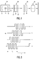
- the image projection apparatus comprises an illumination unit 10 providing a projection light beam 15, here represented by its axis, an image display unit 20 for generating an image, an optical deflection unit 30 for shifting the beam, and a projection lens 40 for projecting the image onto a projection screen 50.
- the illumination unit 10 comprises a lamp 11, for example a ultra high pressure mercury lamp, a reflector 12 and a condenser lens 13 producing a collimated beam.
- the unit 10 may also comprise integrator plates to produce a projection beam having uniform intensity and a cross-section adapted to the display panel to be illuminated, examples of which are disclosed in US-A-5,098,184 and in US-A-5,184,248.
- the image display unit 20 is represented by a single, spatial light modulating liquid crystal display panel 22, preferably a twisted nematic liquid crystalline active matrix panel of the TFT or thin film diode kind.
- the panel is of conventional form comprising a matrix array of m rows and n columns of pixels (i.e. display elements).
- the panel 22 can be a colour panel having a colour micro-filter array aligned with the pixels and forming triplets of red, green and blue pixels.
- the unit 20 may comprise a colour separating system, three display panels for the primary colours red, green and blue and a colour recombination system, as is well known in the art.
- the rows of pixels in the panel 22 are driven, according to an applied video signal, in conventional manner one at a time in sequence from the first row, row 1, to the last row, row m, such that all rows are driven in a field period T f corresponding to the field period of the applied video signal.
- the video signal is of an interlaced type in which odd and even video lines are presented in odd and even field periods respectively. In two successive, odd and even, fields periods, therefore, the rows of pixels are addressed to display odd and even display lines with each row of pixels displaying firstly an odd line and then an even line.
- the number of pixel rows, m corresponds to the number of odd, or even, lines in the video signal
- the m odd lines and m even lines of the video signal are displayed by the m pixel rows over two field periods, i.e. one frame period.
- the units 10, 20 and 30 are accommodated in a housing and the projection screen 50 may be a rear projection screen also accommodated in the housing or a free standing screen or a screen fixed to a wall.
- the optical deflection unit 30 is arranged between the analyser 23 associated with the display panel 22 and the projection screen 50, preferably before the projection lens 40, here shown very schematically.
- the optical deflection unit 30 comprises a polarisation switching element 31 which, depending on the applied electrical drive signal, either allows light to pass through without alteration to its plane of polarisation or rotates the plane of polarisation of the light passing through it by ninety degrees, and a birefringent element 32 which, depending on the polarisation of the light passing through either does or does not produce a vertical positional shift.
- the polarisation switching element 31 is constituted by a panel comprising a layer 34 of electro-optical material and an electrode 37 and segmented electrodes 38 on the substrates 35 and 36 respectively between which the layer 34 is sandwiched.
- the material of the layer 34 is for example a liquid crystalline material such as a ferro-electric liquid crystal material.
- the electrode 38 is divided into a number of strip-electrodes extending parallel to the pixel row direction of the panel 22. If the light from each pixel row of the display panel were to be individually deflected, a complex electrode structure and a large number of drive circuits would be needed.
- the electrode 38 is divided into a small number of strip-electrodes 38a - 38d, each of which is aligned with a respective group of pixel rows of the panel 22, so that the panel 31 comprises a smaller number of horizontal segments, each of which serves to deflect together a number of pixel rows.
- the switching element 31 comprises four horizontal segments, but the number may be increased, for example, to ten.
- Figure 3 shows drive voltage waveforms and relative timings for the four segments, a, b, c and d, of the polarisation switch.
- T f is the field period, i.e. half a videoframe period.
- the segment drive voltages V s for the succeeding segments a, b, c and d are each shifted by a quarter of the field period relative to the preceding one.
- the drive voltages consist of short rectangular pulses which are bipolar to eliminate DC voltages and are synchronised with the video signal to be displayed.
- first and second time intervals each correspond to the field period and are shifted over a quarter field time for the succeeding segments of the polarisation switch.
- the result of the operation of the polarisation switch together with the birefringent element is that the light from the pixel rows belonging to a given switch segment, a, b, c or d, is switched by such segment between two positions, as denoted by the lines A and A' in Figure 2, whereby one of these positions is associated with the even field lines of the displayed image and the other position is associated with the odd field lines.
- the birefringent element 32 is a quartz crystal plate.
- the element provides a transversal shift between the two differently polarised beams from the polarisation switch 31 corresponding to half of the centre-to-centre distance between the pixel rows of the display panel.
- the pixel row images formed by the projection lens on the projection screen are displaced relative to the images of the same pixel rows for the other polarisation direction.
- the deflection unit Seen in the backward direction, from the projection lens to the display panel, causes an apparent lateral displacement in the vertical, column, direction of the pixels. The extent of such displacement is selected, by suitable choice of the shift achieved by the birefringent element 32, so that it is approximately half the centre to centre distance between the pixel rows.
- Figure 4 illustrates schematically an ideal form for a typical part of the projected display image structure to be produced from a few pixel rows belonging to one polarisation switch segment and as would be seen on the projection screen.
- the solid lines represent the apparent positions of projected pixel rows R1, R2 and R3 during a first half frame time (i.e. one field period) and the dotted lines represent the apparent positions of the same projected pixel rows during the second half frame time, here denoted R1', R2' and R3' respectively.
- FIG. 5 which, like Figure 4, shows the apparent positions of parts of pixel rows R1, R2 and R3 in two successive field periods. As can be seen, the position of the row images in the second field period, R1', R2' and R3' substantially overlap the row positions in the first field period. This results in poor display quality, not least because vertical resolution is severely impaired.
- the interlaced pixel row images can be arranged neatly such that one pixel row image of the displaced field fits between two adjacent pixel row images of the undisplaced field.
- the aperture ratio of the panel would then be severely impaired as approximately half of the light incident on the panel would be lost resulting in significantly reduced display brightness.
- the panel 22 is of the kind in which adjacent rows of pixels 25 are separated by comparatively narrow opaque areas so as to maximise light throughput.
- an array of lens elements whose action is to reduce the apparent height of the image of the pixel rows, constituting display lines, in the projected image display.
- the height reduction is relative to the centre to centre spacing of the display lines, (pixel row images) in the projected display.
- the gap between adjacent display lines in one field is correspondingly increased.
- the width reduction is such that the odd display lines fill the gaps between the even display lines without any significant overlap. This is achieved by arranging that the height of a pixel row image is reduced such that it is substantially half the centre to centre spacing between adjacent pixel row images. Consequently, a display line structure like that depicted in Figure 4 is obtained with all the benefits associated with this kind of display panel.
- the lens element array in this embodiment is disposed on the output side of the panel 22 and indicated at 60.
- the lens element array could alternatively be positioned at the input side of the panel, as will be described subsequently.
- Figure 6 shows schematically a cross-section through a part of the panel 22 and the array 60 in this embodiment.
- the transparent, glass, substrates of the panel are indicated at 61 and 62, between which liquid crystal material 63 is disposed, and a few pixels in one column of the array, are here depicted at 25.
- the lens array 60 is preferably arranged close to the plane of the pixels and to this end the lens array is disposed directly on the outer surface of the substrate 62. If the analyser layer 23 were to be carried on this substrate rather than being separated, the lens array could be provided over this layer.
- the lens array 60 comprises elongate, parallel, lens elements 65 extending in the pixel row direction, each lens element 65 being similar and comprising a negative cylindrical lens element aligned with and overlying, a respective row of pixels.
- Other lens profiles for example, comprising contiguous flat portions, could be used.
- the array of lens elements can be provided in the form of a lenticular sheet comprising a moulded plastic sheet of microlenses, in known manner, and secured to the substrate by gluing.
- the lens element action is to increase the divergence of the light from a row of pixels (in the column direction) and form a reduced size virtual image, indicated at 25', of the row of pixels.
- the increased angle of light is inversely proportional to the magnification ratio.
- the projection lens 40 has an adequate aperture to collect this light.
- a limitation to the effectiveness of the lens elements is the thickness of the substrate 62. Some of the light, especially that which has come through the edges of the pixel open area, may then pass through the "wrong" cylindrical lens element 65, and thus some light will appear in the adjacent pixel. The thicker the substrate the worse this effect will be. If the light which passes through the centre of a pixel is considered with a typical illumination cone of F/3 and a refractive index of 1.55 for the glass, then the maximum thickness of the substrate plus lens element is 4.6 times the spacing of the rows of pixels.
- the row spacing for a 3:4 (rows to columns) format 2.8 inch diagonal LC panel is 0.15mm.
- the allowable substrate thickness is around 0.6mm with 0.1mm for the lens element thickness.
- the aperture of the input light may be reduced in the vertical plane (i.e. the plane of Figure 6) and increased in the perpendicular direction to compensate.
- the lens elements 65 may be formed as gradient index lenses in the glass substrate 62 itself.
- the substrate 62 may also comprise a sandwich of materials with substantially different refractive indices, and appropriate profiles, to create the lens elements.
- FIG. 7 is a cross-sectional view through a part of the panel and lens array assembly.
- the lens element array 60 which again may be a moulded plastic lenticular sheet, is secured to the outer surface of the substrate 61 and similarly comprises parallel, elongate, lens elements, here referenced 65', extending in the row direction, each overlying and aligned with, a respective pixel row.
- the lens elements 65' in this case comprise positive cylindrical lenses. The action of these lens elements 65' is to concentrate the input light into the central part of their associated pixels 25.
- the light is concentrated into a strip centred approximately on the central row-direction axis of the pixels which still fills the width of each pixel area but whose height is less than that of the open part of the pixels, the reduction in height being symmetrical about the centre line of the pixel.
- a comparatively narrow band of light at the pixel plane is obtained whose width is less than the height of the pixels and which is centred on the centre line of the pixels.
- the lens elements precede the pixels the problem of light going through the "wrong" lens element, causing a confused picture, is avoided. Instead, some light will fall outside the desired central area of the pixel, giving an approximately Gaussian line profile instead of a top-hat profile.
- An additional advantage of this embodiment is that the active switch devices of the active matrix display panel, for example TFTs or TFDs, located at each pixel area can be arranged to lie in a low light intensity region of the pixel, thus reducing problems due to their photo-sensitive behaviour.
- the lens elements 65' could be provided as gradient index lenses within the glass substrate 61 or formed by making the substrate 61 from a sandwich of materials with appropriate profiles.
- the apparatus may be a full colour projection display apparatus using three separate display panels each operating with a respective one of the three primary colours.
- An example of such apparatus is illustrated schematically in Figure 8.
- Each of the display panels has associated therewith a lens element array either at its output side, as in the Figure 6 embodiment, or at its input side, as in the Figure 7 embodiment.
- a beam of white light from an illumination unit A is incident on a colour-selective reflector 120, for example a dichroic mirror, which reflects, for example, the blue colour component b B and passes the rest of the beam.
- This beam portion reaches a second colour-selective reflector 121 which reflects the green colour component b G and passes the remaining red colour component b R to a reflector 122 which reflects the red beam component toward the projection lens unit C.
- the reflector 122 may be a neutral reflector or a reflector which is optimised for red light.
- the blue beam component is reflected by a neutral or a blue-selective reflector 123 to an LC display panel 22A with an associated lens element array 60. This panel is driven in known manner so that the blue component of the image to be projected appears on this panel.
- the beam component modulated with the blue information reaches the projection lens unit C via colour-selective reflector 124, which passes the blue beam component and reflects the green beam component, and a further colour-selective reflector 125 which reflects the blue beam component.
- the green beam component b G traverses a second LC display panel 22B with an associated lens array 60 where it is modulated with the green colour component and is then reflected to the projection lens unit C successively by the colour-selective reflectors 124 and 125.
- the red beam component b R traverses a third LC display panel 22C with an associated lens array 60 where it is modulated with the red colour component and subsequently reaches the projection lens unit via the colour-selective reflector 125.
- the blue, red and green beam components are superimposed at the input aperture of the lens unit, so that a colour image is created at this aperture which is imaged in a magnified form by this unit on the projection screen, (not shown in Figure 8).
- optical path lengths between the output of the illumination unit A and each display panel 22A, 22B and 22C are preferably equal so that the cross-sections of the red, blue and green beam components are equal at the location of their display panel. Also the optical path lengths between the display panels 22A, 22B and 22C and the input aperture of the projection lens unit are substantially equal so that the differently coloured scenes are satisfactorily superimposed on the projection screen.
- the lenses 129, 130 and 131 arranged in front of the display panels are field lenses which ensure that all light coming from the exit plane of the illumination unit is concentrated in the entrance pupil of the projection lens unit.
- the deflection unit 30, shown as a simple block in Figure 8, is preferably arranged in the combined light path before the projection lens unit C. Then only one such unit is needed and this unit can be positioned at a suitable distance from the display panels.
- the lens elements of the array 60 could comprise an individual lens element for each pixel rather than having elongate lens elements of the kind described.
- the LC display panel, or panels may comprise twisted nematic, ferroelectric, polymer dispersed or other types of LC materials. It is envisaged, however, that other kinds of light modulating matrix display panels could be used.
- an image projection apparatus which comprises an illumination unit, an image display unit comprising a matrix display panel having a row and column array of pixels, a projection lens for projecting an image produced by the display panel on to a screen and an optical deflection unit arranged between the display unit and the projection lens which is operable selectively to shift the light rays from a row of pixels passing therethrough whereby the pixel row images on the screen in one field are displaced and interlaced with the pixel row images of a preceding field.
- the image display unit includes an array of lens elements overlying the array of pixels whose effect is to reduce the height of the image of each pixel row in the projected display so the pixel row images of one field can fill the gaps between adjacent pixel row images of a preceding field without any substantial overlap and display panels having high aperture ratio can be utilised.
Applications Claiming Priority (2)
| Application Number | Priority Date | Filing Date | Title |
|---|---|---|---|
| GBGB9605056.2A GB9605056D0 (en) | 1996-03-09 | 1996-03-09 | Interlaced image projection apparatus |
| GB9605056 | 1996-03-09 |
Publications (2)
| Publication Number | Publication Date |
|---|---|
| EP0794676A2 true EP0794676A2 (de) | 1997-09-10 |
| EP0794676A3 EP0794676A3 (de) | 1998-05-13 |
Family
ID=10790161
Family Applications (1)
| Application Number | Title | Priority Date | Filing Date |
|---|---|---|---|
| EP97200650A Withdrawn EP0794676A3 (de) | 1996-03-09 | 1997-03-05 | Zeilensprung-Bildprojektor |
Country Status (6)
| Country | Link |
|---|---|
| US (1) | US5842762A (de) |
| EP (1) | EP0794676A3 (de) |
| JP (1) | JPH1068997A (de) |
| KR (1) | KR970068572A (de) |
| GB (1) | GB9605056D0 (de) |
| MY (1) | MY132545A (de) |
Cited By (4)
| Publication number | Priority date | Publication date | Assignee | Title |
|---|---|---|---|---|
| WO2005069746A2 (en) * | 2004-01-26 | 2005-08-04 | Lg Electronics Inc. | Apparatus and method for projection type display |
| WO2005094071A1 (en) * | 2004-03-22 | 2005-10-06 | Thomson Licensing | Method and apparatus for improving images provided by spatial light modulated (slm) display systems |
| WO2006043237A1 (en) * | 2004-10-22 | 2006-04-27 | Koninklijke Philips Electronics N.V. | Projector system |
| EP1575307A3 (de) * | 2004-03-10 | 2006-11-02 | Seiko Epson Corporation | Beleuchtungsvorrichtung, Bildanzeigevorrichtung, und Projektor |
Families Citing this family (69)
| Publication number | Priority date | Publication date | Assignee | Title |
|---|---|---|---|---|
| JP3926922B2 (ja) * | 1998-03-23 | 2007-06-06 | オリンパス株式会社 | 画像表示装置 |
| JP3934250B2 (ja) * | 1998-05-11 | 2007-06-20 | オリンパス株式会社 | 画像表示装置 |
| JP4101943B2 (ja) * | 1998-08-07 | 2008-06-18 | オリンパス株式会社 | 画像表示装置 |
| KR100571909B1 (ko) * | 2000-09-21 | 2006-04-17 | 삼성전자주식회사 | 화상투사장치 |
| US7339714B1 (en) | 2001-02-02 | 2008-03-04 | Cheetah Omni, Llc | Variable blazed grating based signal processing |
| US7317465B2 (en) * | 2002-08-07 | 2008-01-08 | Hewlett-Packard Development Company, L.P. | Image display system and method |
| US6963319B2 (en) * | 2002-08-07 | 2005-11-08 | Hewlett-Packard Development Company, L.P. | Image display system and method |
| US7034811B2 (en) * | 2002-08-07 | 2006-04-25 | Hewlett-Packard Development Company, L.P. | Image display system and method |
| US7172288B2 (en) * | 2003-07-31 | 2007-02-06 | Hewlett-Packard Development Company, L.P. | Display device including a spatial light modulator with plural image regions |
| US7030894B2 (en) * | 2002-08-07 | 2006-04-18 | Hewlett-Packard Development Company, L.P. | Image display system and method |
| US7098936B2 (en) * | 2003-03-11 | 2006-08-29 | Hewlett-Packard Development Company, L.P. | Image display system and method including optical scaling |
| US7021766B2 (en) * | 2003-07-22 | 2006-04-04 | Seiko Epson Corporation | Projector |
| US7083283B2 (en) * | 2003-07-22 | 2006-08-01 | Seiko Epson Corporation | Projector |
| US7190380B2 (en) * | 2003-09-26 | 2007-03-13 | Hewlett-Packard Development Company, L.P. | Generating and displaying spatially offset sub-frames |
| US7109981B2 (en) | 2003-07-31 | 2006-09-19 | Hewlett-Packard Development Company, L.P. | Generating and displaying spatially offset sub-frames |
| US7289114B2 (en) * | 2003-07-31 | 2007-10-30 | Hewlett-Packard Development Company, L.P. | Generating and displaying spatially offset sub-frames |
| US7253811B2 (en) * | 2003-09-26 | 2007-08-07 | Hewlett-Packard Development Company, L.P. | Generating and displaying spatially offset sub-frames |
| US7301549B2 (en) * | 2003-10-30 | 2007-11-27 | Hewlett-Packard Development Company, L.P. | Generating and displaying spatially offset sub-frames on a diamond grid |
| US20050093894A1 (en) * | 2003-10-30 | 2005-05-05 | Tretter Daniel R. | Generating an displaying spatially offset sub-frames on different types of grids |
| US7182463B2 (en) * | 2003-12-23 | 2007-02-27 | 3M Innovative Properties Company | Pixel-shifting projection lens assembly to provide optical interlacing for increased addressability |
| US7355612B2 (en) * | 2003-12-31 | 2008-04-08 | Hewlett-Packard Development Company, L.P. | Displaying spatially offset sub-frames with a display device having a set of defective display pixels |
| US6984040B2 (en) * | 2004-01-20 | 2006-01-10 | Hewlett-Packard Development Company, L.P. | Synchronizing periodic variation of a plurality of colors of light and projection of a plurality of sub-frame images |
| US7086736B2 (en) * | 2004-01-20 | 2006-08-08 | Hewlett-Packard Development Company, L.P. | Display system with sequential color and wobble device |
| US7463272B2 (en) * | 2004-01-30 | 2008-12-09 | Hewlett-Packard Development Company, L.P. | Generating and displaying spatially offset sub-frames |
| US7483044B2 (en) * | 2004-01-30 | 2009-01-27 | Hewlett-Packard Development Company, L.P. | Displaying sub-frames at spatially offset positions on a circle |
| US7023449B2 (en) * | 2004-04-30 | 2006-04-04 | Hewlett-Packard Development Company, L.P. | Displaying least significant color image bit-planes in less than all image sub-frame locations |
| US7274346B2 (en) * | 2004-06-01 | 2007-09-25 | Eastman Kodak Company | Uniformity and brightness measurement in OLED displays |
| US7466291B2 (en) * | 2005-03-15 | 2008-12-16 | Niranjan Damera-Venkata | Projection of overlapping single-color sub-frames onto a surface |
| US7443364B2 (en) * | 2005-03-15 | 2008-10-28 | Hewlett-Packard Development Company, L.P. | Projection of overlapping sub-frames onto a surface |
| US9282335B2 (en) | 2005-03-15 | 2016-03-08 | Hewlett-Packard Development Company, L.P. | System and method for coding image frames |
| US7407295B2 (en) * | 2005-07-26 | 2008-08-05 | Niranjan Damera-Venkata | Projection of overlapping sub-frames onto a surface using light sources with different spectral distributions |
| US7387392B2 (en) * | 2005-09-06 | 2008-06-17 | Simon Widdowson | System and method for projecting sub-frames onto a surface |
| US20070091277A1 (en) * | 2005-10-26 | 2007-04-26 | Niranjan Damera-Venkata | Luminance based multiple projector system |
| US7470032B2 (en) * | 2005-10-27 | 2008-12-30 | Hewlett-Packard Development Company, L.P. | Projection of overlapping and temporally offset sub-frames onto a surface |
| US20070097017A1 (en) * | 2005-11-02 | 2007-05-03 | Simon Widdowson | Generating single-color sub-frames for projection |
| US20070132967A1 (en) * | 2005-12-09 | 2007-06-14 | Niranjan Damera-Venkata | Generation of image data subsets |
| US7559661B2 (en) | 2005-12-09 | 2009-07-14 | Hewlett-Packard Development Company, L.P. | Image analysis for generation of image data subsets |
| US20070133087A1 (en) * | 2005-12-09 | 2007-06-14 | Simon Widdowson | Generation of image data subsets |
| US20070133794A1 (en) * | 2005-12-09 | 2007-06-14 | Cloutier Frank L | Projection of overlapping sub-frames onto a surface |
| US20070132965A1 (en) * | 2005-12-12 | 2007-06-14 | Niranjan Damera-Venkata | System and method for displaying an image |
| US7499214B2 (en) * | 2006-03-20 | 2009-03-03 | Hewlett-Packard Development Company, L.P. | Ambient light absorbing screen |
| US7854518B2 (en) * | 2006-06-16 | 2010-12-21 | Hewlett-Packard Development Company, L.P. | Mesh for rendering an image frame |
| US7800628B2 (en) * | 2006-06-16 | 2010-09-21 | Hewlett-Packard Development Company, L.P. | System and method for generating scale maps |
| US20070291184A1 (en) * | 2006-06-16 | 2007-12-20 | Michael Harville | System and method for displaying images |
| US7907792B2 (en) | 2006-06-16 | 2011-03-15 | Hewlett-Packard Development Company, L.P. | Blend maps for rendering an image frame |
| US9137504B2 (en) | 2006-06-16 | 2015-09-15 | Hewlett-Packard Development Company, L.P. | System and method for projecting multiple image streams |
| US20080002160A1 (en) * | 2006-06-30 | 2008-01-03 | Nelson Liang An Chang | System and method for generating and displaying sub-frames with a multi-projector system |
| US20080024389A1 (en) * | 2006-07-27 | 2008-01-31 | O'brien-Strain Eamonn | Generation, transmission, and display of sub-frames |
| US20080024683A1 (en) * | 2006-07-31 | 2008-01-31 | Niranjan Damera-Venkata | Overlapped multi-projector system with dithering |
| US20080024469A1 (en) * | 2006-07-31 | 2008-01-31 | Niranjan Damera-Venkata | Generating sub-frames for projection based on map values generated from at least one training image |
| JP5037508B2 (ja) | 2006-08-09 | 2012-09-26 | シャープ株式会社 | 液晶表示装置 |
| US20080043209A1 (en) * | 2006-08-18 | 2008-02-21 | Simon Widdowson | Image display system with channel selection device |
| US20080095363A1 (en) * | 2006-10-23 | 2008-04-24 | Dicarto Jeffrey M | System and method for causing distortion in captured images |
| US20080094419A1 (en) * | 2006-10-24 | 2008-04-24 | Leigh Stan E | Generating and displaying spatially offset sub-frames |
| US20080101711A1 (en) * | 2006-10-26 | 2008-05-01 | Antonius Kalker | Rendering engine for forming an unwarped reproduction of stored content from warped content |
| US20080101725A1 (en) * | 2006-10-26 | 2008-05-01 | I-Jong Lin | Image display system configured to update correspondences using arbitrary features |
| US7742011B2 (en) * | 2006-10-31 | 2010-06-22 | Hewlett-Packard Development Company, L.P. | Image display system |
| US7414790B2 (en) * | 2006-11-10 | 2008-08-19 | Genie Lens Technologies, Llc | Ultrathin lens arrays for viewing interlaced images with dual lens structures |
| US7359120B1 (en) * | 2006-11-10 | 2008-04-15 | Genie Lens Technologies, Llc | Manufacture of display devices with ultrathin lens arrays for viewing interlaced images |
| US7307790B1 (en) | 2006-11-10 | 2007-12-11 | Genie Lens Technologies, Llc | Ultrathin lens arrays for viewing interlaced images |
| US8132920B2 (en) | 2007-03-19 | 2012-03-13 | Motorola Mobility, Inc. | Thin microprojector with switched beam bender and method of operating the same |
| US8279375B2 (en) * | 2007-04-16 | 2012-10-02 | Sharp Kabushiki Kaisha | Display apparatus, driving apparatus of display apparatus, and electronic device |
| US7986356B2 (en) * | 2007-07-25 | 2011-07-26 | Hewlett-Packard Development Company, L.P. | System and method for determining a gamma curve of a display device |
| US20090027504A1 (en) * | 2007-07-25 | 2009-01-29 | Suk Hwan Lim | System and method for calibrating a camera |
| US7480100B1 (en) | 2007-10-15 | 2009-01-20 | Genie Lens Technologies, Llc | Lenticular devices using sets of lenses to display paired sets of interlaces of images |
| US20090257030A1 (en) * | 2008-04-10 | 2009-10-15 | Motorola, Inc. | Image projector with time-sequential interlacing |
| US8328365B2 (en) | 2009-04-30 | 2012-12-11 | Hewlett-Packard Development Company, L.P. | Mesh for mapping domains based on regularized fiducial marks |
| US9235575B1 (en) | 2010-03-08 | 2016-01-12 | Hewlett-Packard Development Company, L.P. | Systems and methods using a slideshow generator |
| TWI741524B (zh) * | 2020-03-10 | 2021-10-01 | 友達光電股份有限公司 | 顯示裝置 |
Citations (5)
| Publication number | Priority date | Publication date | Assignee | Title |
|---|---|---|---|---|
| FR2611389A1 (fr) * | 1987-02-27 | 1988-09-02 | Thomson Csf | Dispositif imageur matriciel a cristaux liquides a resolution doublee par birefringence |
| EP0444872A2 (de) * | 1990-02-26 | 1991-09-04 | Sharp Kabushiki Kaisha | Flüssigkristallanzeigevorrichtung |
| US5101279A (en) * | 1989-12-14 | 1992-03-31 | Canon Kabushiki Kaisha | Liquid crystal display apparatus having lenticular elements oriented in relation to LC pixel aperture dimensions |
| EP0606162A2 (de) * | 1993-01-07 | 1994-07-13 | Sony Corporation | Bildanzeigesystem mit Mosaikmustern aus Pixeln |
| US5463434A (en) * | 1993-04-26 | 1995-10-31 | Sanyo Electric Co., Ltd. | Video projector with a plurality of projection devices |
Family Cites Families (8)
| Publication number | Priority date | Publication date | Assignee | Title |
|---|---|---|---|---|
| NL8901077A (nl) * | 1989-04-28 | 1990-11-16 | Koninkl Philips Electronics Nv | Optische belichtingsstelsel en projectie-apparaat voorzien van een dergelijk stelsel. |
| US5184248A (en) * | 1990-07-16 | 1993-02-02 | U.S. Philips Corporation | Image projection apparatus |
| US5583694A (en) * | 1992-07-14 | 1996-12-10 | Nippon Telegraph And Telephone Corporation | Optical element and optical axis displacement device using the same |
| BE1007993A3 (nl) * | 1993-12-17 | 1995-12-05 | Philips Electronics Nv | Belichtingsstelsel voor een kleurenbeeldprojectie-inrichting en circulaire polarisator geschikt voor toepassing in een dergelijk belichtingsstelsel en kleurenbeeldprojectie-inrichting bevattende een dergelijk belichtingsstelsel met circulaire polarisator. |
| GB9409707D0 (en) * | 1994-05-14 | 1994-07-06 | Philips Electronics Uk Ltd | Liquid crystal projection display systems |
| DE69535145T2 (de) * | 1994-06-01 | 2007-06-14 | Koninklijke Philips Electronics N.V. | Beleuchtungsgerät mit hohem wirkungsgrad und dieses gerät enthaltende projektionseinrichtung |
| US5537256A (en) * | 1994-10-25 | 1996-07-16 | Fergason; James L. | Electronic dithering system using birefrigence for optical displays and method |
| US5727860A (en) * | 1996-04-04 | 1998-03-17 | U.S. Philips Corporation | Interlaced image projection apparatus |
-
1996
- 1996-03-09 GB GBGB9605056.2A patent/GB9605056D0/en active Pending
-
1997
- 1997-03-05 EP EP97200650A patent/EP0794676A3/de not_active Withdrawn
- 1997-03-07 MY MYPI97000966A patent/MY132545A/en unknown
- 1997-03-10 KR KR1019970007943A patent/KR970068572A/ko not_active Application Discontinuation
- 1997-03-10 US US08/813,417 patent/US5842762A/en not_active Expired - Fee Related
- 1997-03-10 JP JP9054743A patent/JPH1068997A/ja active Pending
Patent Citations (5)
| Publication number | Priority date | Publication date | Assignee | Title |
|---|---|---|---|---|
| FR2611389A1 (fr) * | 1987-02-27 | 1988-09-02 | Thomson Csf | Dispositif imageur matriciel a cristaux liquides a resolution doublee par birefringence |
| US5101279A (en) * | 1989-12-14 | 1992-03-31 | Canon Kabushiki Kaisha | Liquid crystal display apparatus having lenticular elements oriented in relation to LC pixel aperture dimensions |
| EP0444872A2 (de) * | 1990-02-26 | 1991-09-04 | Sharp Kabushiki Kaisha | Flüssigkristallanzeigevorrichtung |
| EP0606162A2 (de) * | 1993-01-07 | 1994-07-13 | Sony Corporation | Bildanzeigesystem mit Mosaikmustern aus Pixeln |
| US5463434A (en) * | 1993-04-26 | 1995-10-31 | Sanyo Electric Co., Ltd. | Video projector with a plurality of projection devices |
Cited By (8)
| Publication number | Priority date | Publication date | Assignee | Title |
|---|---|---|---|---|
| WO2005069746A2 (en) * | 2004-01-26 | 2005-08-04 | Lg Electronics Inc. | Apparatus and method for projection type display |
| WO2005069746A3 (en) * | 2004-01-26 | 2007-05-03 | Lg Electronics Inc | Apparatus and method for projection type display |
| US7237902B2 (en) | 2004-01-26 | 2007-07-03 | Lg Electronics Inc. | Apparatus and method for projection type display |
| KR100820831B1 (ko) * | 2004-01-26 | 2008-04-11 | 엘지전자 주식회사 | 투사형 디스플레이 장치 및 방법 |
| EP1575307A3 (de) * | 2004-03-10 | 2006-11-02 | Seiko Epson Corporation | Beleuchtungsvorrichtung, Bildanzeigevorrichtung, und Projektor |
| WO2005094071A1 (en) * | 2004-03-22 | 2005-10-06 | Thomson Licensing | Method and apparatus for improving images provided by spatial light modulated (slm) display systems |
| US7605832B2 (en) | 2004-03-22 | 2009-10-20 | Thomson Licensing | Method and apparatus for improving images provided by spatial light modulated (SLM) display systems |
| WO2006043237A1 (en) * | 2004-10-22 | 2006-04-27 | Koninklijke Philips Electronics N.V. | Projector system |
Also Published As
| Publication number | Publication date |
|---|---|
| US5842762A (en) | 1998-12-01 |
| GB9605056D0 (en) | 1996-05-08 |
| MY132545A (en) | 2007-10-31 |
| EP0794676A3 (de) | 1998-05-13 |
| JPH1068997A (ja) | 1998-03-10 |
| KR970068572A (ko) | 1997-10-13 |
Similar Documents
| Publication | Publication Date | Title |
|---|---|---|
| US5842762A (en) | Interlaced image projection apparatus | |
| EP0913059B1 (de) | Zeilensprung-farbbildprojektor | |
| JP3940456B2 (ja) | 自動立体ディスプレー装置 | |
| JP2939826B2 (ja) | 投影表示装置 | |
| US6637888B1 (en) | Full color rear screen projection system using a single monochrome TFT LCD panel | |
| JP2004062208A (ja) | 画素移動手段を具備する高解像度ディスプレイ | |
| JPH04316296A (ja) | カラー表示装置及びこの装置におけるライトバルブアドレス指定回路 | |
| JPH03140920A (ja) | 投写型表示装置及び該投写型表示装置に用いる液晶表示装置 | |
| JP4052803B2 (ja) | 画像表示装置 | |
| US5727860A (en) | Interlaced image projection apparatus | |
| JP5367046B2 (ja) | 自動立体ディスプレー装置 | |
| JP2004205919A (ja) | 投射型立体表示装置 | |
| US8162485B2 (en) | Intermediate image formation optical system, image formation device, and methods thereof | |
| US5278681A (en) | Combined color and monochrome display | |
| JP3722204B2 (ja) | 投影型画像表示装置 | |
| US6817718B2 (en) | Projection type optical display system | |
| JP2006058588A (ja) | 光学デバイス、光学装置、表示装置及び立体画像表示装置 | |
| EP0601666A1 (de) | Sequentielle Lichtventil-Farbanzeigevorrichtung | |
| JPH0954554A (ja) | 表示装置および方法 | |
| JPH1055026A (ja) | 投射型カラー表示装置 | |
| JPS6041086A (ja) | 液晶カラ−プロジエクシヨン装置 | |
| JP2004205917A (ja) | 投射型表示装置 | |
| JP2006235145A (ja) | 光学デバイス、光学装置、表示装置及び立体画像表示装置 | |
| US6803902B2 (en) | Variable rate row addressing method | |
| JPH09265106A (ja) | 液晶ディスプレイパネルおよび投射型液晶表示装置 |
Legal Events
| Date | Code | Title | Description |
|---|---|---|---|
| PUAI | Public reference made under article 153(3) epc to a published international application that has entered the european phase |
Free format text: ORIGINAL CODE: 0009012 |
|
| AK | Designated contracting states |
Kind code of ref document: A2 Designated state(s): DE FR GB |
|
| PUAL | Search report despatched |
Free format text: ORIGINAL CODE: 0009013 |
|
| AK | Designated contracting states |
Kind code of ref document: A3 Designated state(s): DE FR GB |
|
| RAP3 | Party data changed (applicant data changed or rights of an application transferred) |
Owner name: KONINKLIJKE PHILIPS ELECTRONICS N.V. |
|
| 17P | Request for examination filed |
Effective date: 19981113 |
|
| STAA | Information on the status of an ep patent application or granted ep patent |
Free format text: STATUS: THE APPLICATION HAS BEEN WITHDRAWN |
|
| 18W | Application withdrawn |
Withdrawal date: 20000803 |