EP0792388B1 - Method for directly depositing metal containing patterned films - Google Patents
Method for directly depositing metal containing patterned films Download PDFInfo
- Publication number
- EP0792388B1 EP0792388B1 EP95936402A EP95936402A EP0792388B1 EP 0792388 B1 EP0792388 B1 EP 0792388B1 EP 95936402 A EP95936402 A EP 95936402A EP 95936402 A EP95936402 A EP 95936402A EP 0792388 B1 EP0792388 B1 EP 0792388B1
- Authority
- EP
- European Patent Office
- Prior art keywords
- metal
- metal complex
- film
- substrate
- ligand
- Prior art date
- Legal status (The legal status is an assumption and is not a legal conclusion. Google has not performed a legal analysis and makes no representation as to the accuracy of the status listed.)
- Expired - Lifetime
Links
- 229910052751 metal Inorganic materials 0.000 title claims description 101
- 239000002184 metal Substances 0.000 title claims description 101
- 238000000034 method Methods 0.000 title claims description 96
- 238000000151 deposition Methods 0.000 title claims description 17
- 150000004696 coordination complex Chemical class 0.000 claims description 164
- 239000003446 ligand Substances 0.000 claims description 89
- 239000000758 substrate Substances 0.000 claims description 73
- 239000000463 material Substances 0.000 claims description 71
- 239000012298 atmosphere Substances 0.000 claims description 33
- 238000006552 photochemical reaction Methods 0.000 claims description 28
- 230000005670 electromagnetic radiation Effects 0.000 claims description 27
- 230000005281 excited state Effects 0.000 claims description 25
- 125000004429 atom Chemical group 0.000 claims description 19
- 238000010521 absorption reaction Methods 0.000 claims description 18
- 238000006243 chemical reaction Methods 0.000 claims description 18
- 229910044991 metal oxide Inorganic materials 0.000 claims description 17
- 150000004706 metal oxides Chemical class 0.000 claims description 17
- 150000002500 ions Chemical class 0.000 claims description 13
- QVGXLLKOCUKJST-UHFFFAOYSA-N atomic oxygen Chemical compound [O] QVGXLLKOCUKJST-UHFFFAOYSA-N 0.000 claims description 11
- 229910052760 oxygen Inorganic materials 0.000 claims description 11
- 239000001301 oxygen Substances 0.000 claims description 11
- 238000012546 transfer Methods 0.000 claims description 10
- 230000001464 adherent effect Effects 0.000 claims description 9
- 239000000126 substance Substances 0.000 claims description 9
- JCXJVPUVTGWSNB-UHFFFAOYSA-N Nitrogen dioxide Chemical compound O=[N]=O JCXJVPUVTGWSNB-UHFFFAOYSA-N 0.000 claims description 8
- 238000000137 annealing Methods 0.000 claims description 7
- 125000004432 carbon atom Chemical group C* 0.000 claims description 7
- 125000000962 organic group Chemical group 0.000 claims description 7
- UFHFLCQGNIYNRP-UHFFFAOYSA-N Hydrogen Chemical compound [H][H] UFHFLCQGNIYNRP-UHFFFAOYSA-N 0.000 claims description 6
- 239000000203 mixture Substances 0.000 claims description 6
- 150000001412 amines Chemical class 0.000 claims description 5
- 125000005595 acetylacetonate group Chemical group 0.000 claims description 4
- 229910052739 hydrogen Inorganic materials 0.000 claims description 4
- 239000001257 hydrogen Substances 0.000 claims description 4
- 241001120493 Arene Species 0.000 claims description 3
- 125000003545 alkoxy group Chemical group 0.000 claims description 3
- 125000000217 alkyl group Chemical group 0.000 claims description 3
- 150000004945 aromatic hydrocarbons Chemical class 0.000 claims description 3
- RBFQJDQYXXHULB-UHFFFAOYSA-N arsane Chemical class [AsH3] RBFQJDQYXXHULB-UHFFFAOYSA-N 0.000 claims description 3
- 125000003118 aryl group Chemical group 0.000 claims description 3
- IVRMZWNICZWHMI-UHFFFAOYSA-N azide group Chemical group [N-]=[N+]=[N-] IVRMZWNICZWHMI-UHFFFAOYSA-N 0.000 claims description 3
- 150000007942 carboxylates Chemical class 0.000 claims description 3
- 150000004985 diamines Chemical class 0.000 claims description 3
- 125000002534 ethynyl group Chemical class [H]C#C* 0.000 claims description 3
- 150000003003 phosphines Chemical class 0.000 claims description 3
- 150000003222 pyridines Chemical class 0.000 claims description 3
- 230000005855 radiation Effects 0.000 claims description 3
- 229910002651 NO3 Inorganic materials 0.000 claims description 2
- NHNBFGGVMKEFGY-UHFFFAOYSA-N Nitrate Chemical compound [O-][N+]([O-])=O NHNBFGGVMKEFGY-UHFFFAOYSA-N 0.000 claims description 2
- MWUXSHHQAYIFBG-UHFFFAOYSA-N Nitric oxide Chemical group O=[N] MWUXSHHQAYIFBG-UHFFFAOYSA-N 0.000 claims description 2
- 150000001540 azides Chemical class 0.000 claims description 2
- 125000005587 carbonate group Chemical group 0.000 claims description 2
- 125000002915 carbonyl group Chemical group [*:2]C([*:1])=O 0.000 claims description 2
- 125000004093 cyano group Chemical group *C#N 0.000 claims description 2
- 229910052736 halogen Inorganic materials 0.000 claims description 2
- 150000002367 halogens Chemical class 0.000 claims description 2
- 125000004356 hydroxy functional group Chemical group O* 0.000 claims description 2
- 125000001810 isothiocyanato group Chemical group *N=C=S 0.000 claims description 2
- 125000000449 nitro group Chemical group [O-][N+](*)=O 0.000 claims description 2
- 125000002813 thiocarbonyl group Chemical group *C(*)=S 0.000 claims description 2
- 125000000858 thiocyanato group Chemical group *SC#N 0.000 claims description 2
- 230000001131 transforming effect Effects 0.000 claims 3
- 125000000816 ethylene group Chemical class [H]C([H])([*:1])C([H])([H])[*:2] 0.000 claims 1
- 239000010408 film Substances 0.000 description 136
- 230000008569 process Effects 0.000 description 25
- PXHVJJICTQNCMI-UHFFFAOYSA-N nickel Substances [Ni] PXHVJJICTQNCMI-UHFFFAOYSA-N 0.000 description 20
- 238000004528 spin coating Methods 0.000 description 14
- 150000002739 metals Chemical class 0.000 description 11
- YMWUJEATGCHHMB-UHFFFAOYSA-N Dichloromethane Chemical compound ClCCl YMWUJEATGCHHMB-UHFFFAOYSA-N 0.000 description 9
- 238000010894 electron beam technology Methods 0.000 description 7
- XUIMIQQOPSSXEZ-UHFFFAOYSA-N Silicon Chemical compound [Si] XUIMIQQOPSSXEZ-UHFFFAOYSA-N 0.000 description 6
- 239000010949 copper Substances 0.000 description 6
- 238000000059 patterning Methods 0.000 description 6
- 229910052710 silicon Inorganic materials 0.000 description 6
- 239000010703 silicon Substances 0.000 description 6
- RYGMFSIKBFXOCR-UHFFFAOYSA-N Copper Chemical group [Cu] RYGMFSIKBFXOCR-UHFFFAOYSA-N 0.000 description 5
- 229910052802 copper Inorganic materials 0.000 description 5
- XLYOFNOQVPJJNP-ZSJDYOACSA-N heavy water Substances [2H]O[2H] XLYOFNOQVPJJNP-ZSJDYOACSA-N 0.000 description 5
- 239000002904 solvent Substances 0.000 description 5
- 239000006227 byproduct Substances 0.000 description 4
- 239000007795 chemical reaction product Substances 0.000 description 4
- BERDEBHAJNAUOM-UHFFFAOYSA-N copper(I) oxide Inorganic materials [Cu]O[Cu] BERDEBHAJNAUOM-UHFFFAOYSA-N 0.000 description 4
- KRFJLUBVMFXRPN-UHFFFAOYSA-N cuprous oxide Chemical compound [O-2].[Cu+].[Cu+] KRFJLUBVMFXRPN-UHFFFAOYSA-N 0.000 description 4
- QDOXWKRWXJOMAK-UHFFFAOYSA-N dichromium trioxide Chemical compound O=[Cr]O[Cr]=O QDOXWKRWXJOMAK-UHFFFAOYSA-N 0.000 description 4
- 238000010884 ion-beam technique Methods 0.000 description 4
- 230000007246 mechanism Effects 0.000 description 4
- 239000010409 thin film Substances 0.000 description 4
- CSCPPACGZOOCGX-UHFFFAOYSA-N Acetone Chemical compound CC(C)=O CSCPPACGZOOCGX-UHFFFAOYSA-N 0.000 description 3
- YXFVVABEGXRONW-UHFFFAOYSA-N Toluene Chemical compound CC1=CC=CC=C1 YXFVVABEGXRONW-UHFFFAOYSA-N 0.000 description 3
- 230000004075 alteration Effects 0.000 description 3
- 238000010420 art technique Methods 0.000 description 3
- 239000004020 conductor Substances 0.000 description 3
- 230000008021 deposition Effects 0.000 description 3
- 238000010586 diagram Methods 0.000 description 3
- 238000010438 heat treatment Methods 0.000 description 3
- 238000004519 manufacturing process Methods 0.000 description 3
- 238000012986 modification Methods 0.000 description 3
- 230000004048 modification Effects 0.000 description 3
- 125000001997 phenyl group Chemical group [H]C1=C([H])C([H])=C(*)C([H])=C1[H] 0.000 description 3
- 239000010453 quartz Substances 0.000 description 3
- 239000004065 semiconductor Substances 0.000 description 3
- VYPSYNLAJGMNEJ-UHFFFAOYSA-N silicon dioxide Inorganic materials O=[Si]=O VYPSYNLAJGMNEJ-UHFFFAOYSA-N 0.000 description 3
- VGGSQFUCUMXWEO-UHFFFAOYSA-N Ethene Chemical compound C=C VGGSQFUCUMXWEO-UHFFFAOYSA-N 0.000 description 2
- 239000005977 Ethylene Substances 0.000 description 2
- 230000009471 action Effects 0.000 description 2
- 229910052782 aluminium Inorganic materials 0.000 description 2
- XAGFODPZIPBFFR-UHFFFAOYSA-N aluminium Chemical compound [Al] XAGFODPZIPBFFR-UHFFFAOYSA-N 0.000 description 2
- PNEYBMLMFCGWSK-UHFFFAOYSA-N aluminium oxide Inorganic materials [O-2].[O-2].[O-2].[Al+3].[Al+3] PNEYBMLMFCGWSK-UHFFFAOYSA-N 0.000 description 2
- 238000003776 cleavage reaction Methods 0.000 description 2
- 150000001875 compounds Chemical class 0.000 description 2
- 229910052593 corundum Inorganic materials 0.000 description 2
- 239000003431 cross linking reagent Substances 0.000 description 2
- 238000002425 crystallisation Methods 0.000 description 2
- 230000008025 crystallization Effects 0.000 description 2
- 230000008020 evaporation Effects 0.000 description 2
- 238000001704 evaporation Methods 0.000 description 2
- 230000000873 masking effect Effects 0.000 description 2
- 229910052976 metal sulfide Inorganic materials 0.000 description 2
- 229910052759 nickel Inorganic materials 0.000 description 2
- 125000002524 organometallic group Chemical group 0.000 description 2
- 229920002120 photoresistant polymer Polymers 0.000 description 2
- 239000000047 product Substances 0.000 description 2
- 150000003254 radicals Chemical class 0.000 description 2
- 230000007017 scission Effects 0.000 description 2
- 238000005245 sintering Methods 0.000 description 2
- 239000007787 solid Substances 0.000 description 2
- RXJKFRMDXUJTEX-UHFFFAOYSA-N triethylphosphine Chemical compound CCP(CC)CC RXJKFRMDXUJTEX-UHFFFAOYSA-N 0.000 description 2
- XLYOFNOQVPJJNP-UHFFFAOYSA-N water Substances O XLYOFNOQVPJJNP-UHFFFAOYSA-N 0.000 description 2
- 229910001845 yogo sapphire Inorganic materials 0.000 description 2
- OBETXYAYXDNJHR-UHFFFAOYSA-N 2-Ethylhexanoic acid Chemical compound CCCCC(CC)C(O)=O OBETXYAYXDNJHR-UHFFFAOYSA-N 0.000 description 1
- VEQPNABPJHWNSG-UHFFFAOYSA-N Nickel(2+) Chemical class [Ni+2] VEQPNABPJHWNSG-UHFFFAOYSA-N 0.000 description 1
- 241000315040 Omura Species 0.000 description 1
- RTAQQCXQSZGOHL-UHFFFAOYSA-N Titanium Chemical compound [Ti] RTAQQCXQSZGOHL-UHFFFAOYSA-N 0.000 description 1
- 229910052768 actinide Inorganic materials 0.000 description 1
- 150000001255 actinides Chemical class 0.000 description 1
- 230000002411 adverse Effects 0.000 description 1
- 239000003513 alkali Substances 0.000 description 1
- 238000013459 approach Methods 0.000 description 1
- 239000011230 binding agent Substances 0.000 description 1
- DWPDSISGRAWLLV-JHZYRPMRSA-L calcium;(1r,4ar,4br,10ar)-1,4a-dimethyl-7-propan-2-yl-2,3,4,4b,5,6,10,10a-octahydrophenanthrene-1-carboxylate Chemical compound [Ca+2].C([C@@H]12)CC(C(C)C)=CC1=CC[C@@H]1[C@]2(C)CCC[C@@]1(C)C([O-])=O.C([C@@H]12)CC(C(C)C)=CC1=CC[C@@H]1[C@]2(C)CCC[C@@]1(C)C([O-])=O DWPDSISGRAWLLV-JHZYRPMRSA-L 0.000 description 1
- SHZIWNPUGXLXDT-UHFFFAOYSA-N caproic acid ethyl ester Natural products CCCCCC(=O)OCC SHZIWNPUGXLXDT-UHFFFAOYSA-N 0.000 description 1
- SLFKPACCQUVAPG-UHFFFAOYSA-N carbon monoxide;nickel;triphenylphosphane Chemical compound O=C=[Ni]=C=O.C1=CC=CC=C1P(C=1C=CC=CC=1)C1=CC=CC=C1.C1=CC=CC=C1P(C=1C=CC=CC=1)C1=CC=CC=C1 SLFKPACCQUVAPG-UHFFFAOYSA-N 0.000 description 1
- 239000003153 chemical reaction reagent Substances 0.000 description 1
- 239000011248 coating agent Substances 0.000 description 1
- 238000000576 coating method Methods 0.000 description 1
- 239000002178 crystalline material Substances 0.000 description 1
- 229910021419 crystalline silicon Inorganic materials 0.000 description 1
- 238000005137 deposition process Methods 0.000 description 1
- 239000003989 dielectric material Substances 0.000 description 1
- 238000009792 diffusion process Methods 0.000 description 1
- 238000003618 dip coating Methods 0.000 description 1
- 238000005530 etching Methods 0.000 description 1
- 125000001495 ethyl group Chemical group [H]C([H])([H])C([H])([H])* 0.000 description 1
- 239000007789 gas Substances 0.000 description 1
- 239000011261 inert gas Substances 0.000 description 1
- 230000000977 initiatory effect Effects 0.000 description 1
- 230000002452 interceptive effect Effects 0.000 description 1
- 239000013067 intermediate product Substances 0.000 description 1
- 230000001678 irradiating effect Effects 0.000 description 1
- 230000031700 light absorption Effects 0.000 description 1
- 230000000670 limiting effect Effects 0.000 description 1
- 229910001092 metal group alloy Inorganic materials 0.000 description 1
- 239000007769 metal material Substances 0.000 description 1
- 229920005588 metal-containing polymer Polymers 0.000 description 1
- SYSQUGFVNFXIIT-UHFFFAOYSA-N n-[4-(1,3-benzoxazol-2-yl)phenyl]-4-nitrobenzenesulfonamide Chemical class C1=CC([N+](=O)[O-])=CC=C1S(=O)(=O)NC1=CC=C(C=2OC3=CC=CC=C3N=2)C=C1 SYSQUGFVNFXIIT-UHFFFAOYSA-N 0.000 description 1
- 229910000480 nickel oxide Inorganic materials 0.000 description 1
- 239000011368 organic material Substances 0.000 description 1
- 230000003647 oxidation Effects 0.000 description 1
- 238000007254 oxidation reaction Methods 0.000 description 1
- GNRSAWUEBMWBQH-UHFFFAOYSA-N oxonickel Chemical compound [Ni]=O GNRSAWUEBMWBQH-UHFFFAOYSA-N 0.000 description 1
- 229910052763 palladium Inorganic materials 0.000 description 1
- 238000000206 photolithography Methods 0.000 description 1
- 238000006303 photolysis reaction Methods 0.000 description 1
- 230000015843 photosynthesis, light reaction Effects 0.000 description 1
- 229910052697 platinum Inorganic materials 0.000 description 1
- 229920000642 polymer Polymers 0.000 description 1
- 229920006254 polymer film Polymers 0.000 description 1
- 239000002243 precursor Substances 0.000 description 1
- 238000012545 processing Methods 0.000 description 1
- 230000001737 promoting effect Effects 0.000 description 1
- 238000000197 pyrolysis Methods 0.000 description 1
- 230000002829 reductive effect Effects 0.000 description 1
- 238000011160 research Methods 0.000 description 1
- 230000000717 retained effect Effects 0.000 description 1
- 238000009987 spinning Methods 0.000 description 1
- 238000005507 spraying Methods 0.000 description 1
- 239000002887 superconductor Substances 0.000 description 1
- 239000010936 titanium Substances 0.000 description 1
- 229910052719 titanium Inorganic materials 0.000 description 1
- 229910052723 transition metal Inorganic materials 0.000 description 1
- 150000003624 transition metals Chemical class 0.000 description 1
- 238000005406 washing Methods 0.000 description 1
Images




Classifications
-
- C—CHEMISTRY; METALLURGY
- C23—COATING METALLIC MATERIAL; COATING MATERIAL WITH METALLIC MATERIAL; CHEMICAL SURFACE TREATMENT; DIFFUSION TREATMENT OF METALLIC MATERIAL; COATING BY VACUUM EVAPORATION, BY SPUTTERING, BY ION IMPLANTATION OR BY CHEMICAL VAPOUR DEPOSITION, IN GENERAL; INHIBITING CORROSION OF METALLIC MATERIAL OR INCRUSTATION IN GENERAL
- C23C—COATING METALLIC MATERIAL; COATING MATERIAL WITH METALLIC MATERIAL; SURFACE TREATMENT OF METALLIC MATERIAL BY DIFFUSION INTO THE SURFACE, BY CHEMICAL CONVERSION OR SUBSTITUTION; COATING BY VACUUM EVAPORATION, BY SPUTTERING, BY ION IMPLANTATION OR BY CHEMICAL VAPOUR DEPOSITION, IN GENERAL
- C23C18/00—Chemical coating by decomposition of either liquid compounds or solutions of the coating forming compounds, without leaving reaction products of surface material in the coating; Contact plating
- C23C18/14—Decomposition by irradiation, e.g. photolysis, particle radiation or by mixed irradiation sources
-
- C—CHEMISTRY; METALLURGY
- C23—COATING METALLIC MATERIAL; COATING MATERIAL WITH METALLIC MATERIAL; CHEMICAL SURFACE TREATMENT; DIFFUSION TREATMENT OF METALLIC MATERIAL; COATING BY VACUUM EVAPORATION, BY SPUTTERING, BY ION IMPLANTATION OR BY CHEMICAL VAPOUR DEPOSITION, IN GENERAL; INHIBITING CORROSION OF METALLIC MATERIAL OR INCRUSTATION IN GENERAL
- C23C—COATING METALLIC MATERIAL; COATING MATERIAL WITH METALLIC MATERIAL; SURFACE TREATMENT OF METALLIC MATERIAL BY DIFFUSION INTO THE SURFACE, BY CHEMICAL CONVERSION OR SUBSTITUTION; COATING BY VACUUM EVAPORATION, BY SPUTTERING, BY ION IMPLANTATION OR BY CHEMICAL VAPOUR DEPOSITION, IN GENERAL
- C23C18/00—Chemical coating by decomposition of either liquid compounds or solutions of the coating forming compounds, without leaving reaction products of surface material in the coating; Contact plating
- C23C18/14—Decomposition by irradiation, e.g. photolysis, particle radiation or by mixed irradiation sources
- C23C18/143—Radiation by light, e.g. photolysis or pyrolysis
-
- H—ELECTRICITY
- H05—ELECTRIC TECHNIQUES NOT OTHERWISE PROVIDED FOR
- H05K—PRINTED CIRCUITS; CASINGS OR CONSTRUCTIONAL DETAILS OF ELECTRIC APPARATUS; MANUFACTURE OF ASSEMBLAGES OF ELECTRICAL COMPONENTS
- H05K3/00—Apparatus or processes for manufacturing printed circuits
- H05K3/10—Apparatus or processes for manufacturing printed circuits in which conductive material is applied to the insulating support in such a manner as to form the desired conductive pattern
- H05K3/105—Apparatus or processes for manufacturing printed circuits in which conductive material is applied to the insulating support in such a manner as to form the desired conductive pattern by conversion of non-conductive material on or in the support into conductive material, e.g. by using an energy beam
Definitions
- This invention relates to methods for fabricating patterned films of metals or metal containing compounds on a substrate.
- the invention has particular application in forming patterned films comprising metal oxides and/or metals.
- Other applications include the interconnection of components on semi-custom chips and the patterning of integrated circuits, either instead of or in conjunction with photo-resist based patterning.
- the methods of the invention may be used in the manufacture of certain VLSI devices.
- United States patent No. 4,952,556, Mantese et al. discloses a method for making patterned films of superconductor materials. The method involves depositing films of a metallo organic material on a substrate and patterning the film with an electron beam, ion beam or laser. The patterning is accomplished by local heating or energy deposit in the film and does not involve a photochemical reaction.
- Various electronic devices can be made by depositing thin patterned films of materials having different electrical characteristics on a substrate.
- Current techniques for manufacturing such devices generally begin with a suitable substrate, such as a wafer of crystalline silicon, on which materials having various electrical characteristics are deposited. These current techniques are expensive because they generally include many steps. Typically, each step involves applying a photo-resist to the surface of the substrate; changing the properties of selected areas of the photo-resist by exposing those areas to light, X-rays or an electron beam; removing either the exposed or unexposed portions of the photo-resist to expose portions of the underlying substrate; chemically treating or depositing a material on the exposed portions of the substrate; and removing the photo-resist.
- a disadvantage of many such prior art techniques is that resolution can be lost in what is essentially a two-stage masking process.
- Some prior art processes include depositing a layer of material on a substrate, applying a photoresist to areas where it is desirable to retain the material, and then etching the material away in places where it is not required.
- This method has the disadvantages set out above and the further disadvantage that the edges of the retained material can be rough or undercut. This can ultimately lead to cracks which can cause the device to fail.
- Japanese patent application No. 1004738 discloses a method for making a patterned film on a substrate.
- the method involves depositing a metallic resinate, together with a photo-crosslinking agent, on a substrate.
- the photo-crosslinking agent is then exposed and developed to yield a pattern which can be reduced to a pattern of metallic wires by sintering.
- This method does not disclose a photochemical reaction which causes a metal complex to convert into a metal containing material, such as metal oxide, on a substrate. It requires a high temperature sintering step which is not necessary in processes according to the present invention.
- Japanese patent application No. 62263973 discloses a method for making a patterned thin metal film.
- the method uses an electron beam to decompose portions of an organometallic thin film to form metals. This method does not involve a photochemical reaction.
- Kestenbaum et al. U.S. patent 5,064,685 discloses a method for making patterns of metals. The method involves applying a metal-organic ink to a substrate. The metal organic ink is then heated with a laser to pyrolize the ink to leave a deposited metal film. This method exposes the substrate to high temperatures and does not allow for the deposition of materials other than metals.
- Some researchers have experimented with photolithography of metal containing polymer films to produce patterns of metals. These methods generally involve patterning a photosensitive polymer film, washing away some parts of the film with a solvent and then reducing the remaining parts of the film to a metal film by pyrolysis. It is hard to produce pure metal films by these techniques.
- This invention provides a method for making a pattern of a metal containing material on a substrate.
- the method includes the steps of: depositing an amorphous film of a metal complex on a surface of a substrate; placing the film in a selected atmosphere; and exposing selected areas of the film to electromagnetic radiation, which is preferably ultraviolet light, or to electron, ion or atom beams to cause the metal complex in the selected areas to undergo a photochemical reaction.
- Electron beams, ion beams or atom beams may be used to practise the invention, if they are able to populate the desired excited state of the metal complex and thus to trigger the photo-chemical reaction.
- the reaction transforms the metal complex in the selected areas into a new metal containing material adherent to the substrate. During exposure the temperature of the substrate is maintained lower than the temperature at which the metal complex decomposes.
- the selected atmosphere comprises oxygen and the new metal containing material is a metal oxide.
- the oxygen comprising atmosphere is preferably air.
- the remaining metal complex is removed from the substrate after the step of exposing the selected areas of the film to electromagnetic radiation or to the electron, ion or atom beams.
- a metal oxide produced according to the invention is reacted with a suitable chemical in a suitable atmosphere to reduce the metal oxide to a metal adherent to the substrate.
- a local temperature of the new material is maintained below an annealing temperature of the new metal containing material throughout the step of exposing the selected areas of the film to electromagnetic radiation or to the electron, ion or atom beams.
- the step of exposing the selected areas is preferably achieved by aligning a mask over the substrate and illuminating that surface of the mask, which is away from said substrate, with electromagnetic radiation, electron, ion or atom beams.
- Another aspect of the invention provides for the deposition of two different materials in a pattern.
- This aspect of the invention involves the steps of depositing an amorphous film of a metal complex on a surface of a substrate; placing the film in a first selected atmosphere; and exposing first selected areas of the film to electromagnetic radiation, which is preferably ultraviolet light, to cause the metal complex in the first selected areas to undergo a photo-chemical reaction.
- electromagnetic radiation which is preferably ultraviolet light
- the reaction transforms the metal complex in the first selected areas into a first new metal containing material adherent to the substrate.
- the film is placed in a second selected atmosphere; and second selected areas of the film are exposed to electromagnetic radiation to cause the metal complex in the second selected areas to undergo a photo-chemical reaction.
- the reaction transforms the metal complex in the second selected areas into volatile components and a second metal containing material adherent to the substrate. Electron, ion or atom beams may also be employed in the first or in the second or in both exposure steps. When the first selected areas are adjacent to the second selected areas, the first and second metal containing materials form a planar structure on the substrate.
- the steps of exposing the first and second selected areas of the film to electromagnetic radiation respectively comprise aligning first first and second masks over the substrate and illuminating surfaces of the masks away from the substrate with electromagnetic radiation, which is preferably ultraviolet radiation, or with the electron, ion or atom beams.
- the metal complex comprises one or more metal atoms bonded to one or more ligands.
- at least one of the ligands is bonded to the metal complex by a chemical bond which is broken by the absorption of electromagnetic radiation.
- the complex becomes thermally unstable when this ligand is removed.
- at least one of the ligands comprises an azide group.
- the ligands are selected from the group consisting of: acetylacetonates (both substituted and unsubstituted); dialkyldithiocarbamates; carboxylate; pyridines; amines; diamines; arsines; diarsenes; phosphines; diphosphenes; arenes; alkoxy ligands; alkyl ligands; and aryl ligands.
- the ligands are preferably small and do not comprise any organic groups containing more than 26 carbon atoms. Most preferably, if the ligands do not include phenyl groups then the ligands do not comprise any organic groups containing more than 12 carbon atoms.
- This invention provides a process for making a structure comprising a film on a substrate.
- the film is patterned and has areas comprising different materials. Unlike most prior art processes, the process does not require the steps of applying and removing a photo-resist or similar material to the structure being fabricated.
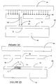
- the process of the invention involves applying an amorphous film 40 of a metal complex 41 to a substrate 44 and then selectively converting portions of film 40 to different metal containing materials by photo-chemically reacting selected portions of film 40 in a selected atmosphere.
- the metal complexes which may be used to practise the invention are discussed below.
- the material of substrate 44 may be any one of a wide variety of materials which are compatible for the purposes of the invention with film 40 and the metal complex 41 .
- Substrate 44 should be a material which does not impair the photochemical reactions described below, is capable of adhering to film 40 . If the device being manufactured will be exposed to large thermal variations then substrate 44 should have a coefficient of expansion reasonably well matched to that of the material to be deposited. However, because this invention does not require high temperature process steps, it is not as important for the coefficient of expansion of the substrate to be matched to that of the material being deposited as it is in prior art methods.
- Substrate 44 may be, for example, a clean silicon wafer or chip which may be etched or may have an oxide coating, or a quartz slide.
- FIGS 1 and 2A through 2E illustrate the use of the process of the invention to create a patterned film.
- the process begins (step 20 ) by applying an amorphous film 40 of a selected photo-reactive metal complex 41 to a substrate 44 .
- Film 40 may generally be conveniently applied to substrate 44 by spin-coating and typically has a thickness of between 20 nm and several ⁇ m. The thickness depends upon the desired end product. Where the goal is to deposit a very thin layer of a material, such as titanium, for use as a binding agent then film 40 should be very thin, for example, in the range of 20-50 nm. Where the goal is to deposit a conductor approximately 0.5 ⁇ m thick then film 40 is most preferably in the range of approximately 2-5 ⁇ m thick.
- film 40 preferably has a thickness between these ranges. In any case, it is best that film 40 be as thin as possible to achieve the desired goal. It is easier for reaction by-products to diffuse out of thin films 40 and it is easier to completely expose thin films 40 to light.
- the spin coating is carried out by placing a drop of a solution of metal complex 41 in a chemically compatible solvent onto substrate 44 and then rotating substrate 44 .
- a drop of metal complex 41 in solution may be dropped on a spinning substrate.
- the spin coating of metal complex 41 on a substrate 44 may generally be accomplished with the same equipment used to apply films of photoresist in prior art processes.
- a commercial spin coating machine of a type available from Headway Research Inc. of 3713 Forest Lane, Garland Texas may be used.
- the thickness of film 40 may be adjusted, as is known in the spin coating art, by adjusting the rate of spin of the substrate, the viscosity of the solution,and the concentration of the solution. In some cases, the rate of feed of the solution is also a factor.
- the spin coating may be carried out at room temperature.
- metal complex 41 is Ni(CO) 2 (PPh 3 ) 2 (wherein Ph represents a phenyl group)
- the solvent used may be methylene chloride.
- a solution having a concentration of 1.57 ⁇ 10 -2 M and a spin speed of 725 R.P.M. a film having a thickness of approximately 90 nm (90 monolayers) is formed.
- the resulting film 40 is allowed to dry.
- a first mask 48 is aligned over film 40 and film 40 is placed in a first atmosphere 50 .
- First mask 48 has both opaque areas and transparent areas 58 .
- the transparent areas 58 correspond to areas 60 in which it is desired to convert film 40 into a different material.
- step 24 the side of mask 48 away from film 40 is exposed to light from a light source 54 .
- Light source 54 emits light of a wavelength (typically in the blue or ultraviolet wavelengths) which is absorbed by metal complex 41 . In general, shorter wavelengths are preferred because short wavelengths offer higher pattern resolution. The resolution of the process is generally limited by diffraction of the light from light source 54 around mask 48 .
- light source 54 may be a Xe lamp or a Hg vapour lamp, such as a 100 W high pressure Hg vapour lamp in an OrielTM housing equipped with condenser lenses and a 10 cm water filter with quartz optics.
- a HeCd laser emitting light at 325 nm and/or 416 nm has useful properties for use as a light source in association with many metal complexes 41 .
- Light from light source 54 passes through transparent areas 58 in first mask 48 and illuminates areas 60 of film 40 .
- Other areas 61 of film 40 are in the shadow of first mask 48 and are not illuminated.
- Metal complex 41 in illuminated areas 60 of film 40 reacts under the action of the light in first atmosphere 50 in a low temperature photochemical reaction to form a first new material 70 which is adherent to substrate 44 .
- the first atmosphere may be air and first new material 70 may be a metal oxide.
- metal complex 41 does not react with first atmosphere 50 because the light necessary for the chemical reaction is not present.
- the time required to complete the photochemical reaction varies with the thickness of the film and the intensity of the applied light.
- the speed varies from metal complex to metal complex. Typical exposure times vary between 2 minutes in light from a 50 W Hg vapour lamp and several hours under light from a 100 W Hg vapour lamp.
- Light from light source 54 should be as intense as possible to speed the reaction without interfering with the reaction itself.
- the light used should not be so intense as to unduly heat the substrate.
- the temperature of the substrate should be maintained at a temperature lower than the annealing temperature of new material 70 .
- the temperature should also be maintained lower than the temperature at which metal complex 41 thermally decomposes. In most cases the temperature of the substrate should not exceed 320 °C or some lower temperature. It is a feature of the invention that, if necessary, many useful new materials 70 may be deposited at room temperature, which is impossible with most practical prior art processes.
- steps 22 and 24 may be repeated, with different masks in different atmospheres, to form areas of other materials in film 40 .
- film 40 is placed in a second atmosphere 74 and a second mask 76 is aligned over film 40 .
- Second mask 76 is then exposed to light from light source 54 .
- the light passes through transparent areas 58 in second mask 76 and illuminates areas 78 of film 40 .
- metal complex 41 reacts under the action of the light, in the second atmosphere 74 to form a second new material 80 .
- Portions of film 40 in non-illuminated areas 79 of film 40 are unaffected.
- the result, as shown in Figure 2E is a planar structure comprising regions of first new material 70 and second new material 80 .
- film 40 is heated in a selected atmosphere (step 25 ) after step 24 to a temperature at which first new material 70 is stable but metal complex 41 is unstable.
- the areas of film 40 which comprise metal complex 41 react at the increased temperature to form a different material.
- the chemical composition of the areas of film 40 which comprise material 70 are either substantially unaffected by the heating or affected differently by the heating. The result is a film 40 in which areas 60 and areas 61 have different properties.
- Complex 41 may be completely inorganic, organometallic or metal organic.
- M may be an alkali or alkaline earth material (for example Ba), a transition metal (for example Cr), a main group metal (for example Al), or an actinide (for example U).
- metal complex 41 should be as small as possible while having the properties necessary to practise the invention.
- Ligands L may all be identical or may be different. Ligands L are chosen so that complex 41 can be formed and has the properties that: 1) it can be deposited in an amorphous film on a substrate; 2) the amorphous film is stable or, at least, metastable; 3) on absorbing light of a required wavelength in a selected atmosphere the film can be transformed into a different metal containing material through a photo induced chemical reaction; and, 4) any byproducts of the photo induced chemical reaction should normally be sufficiently volatile to be removed from the film.
- metal complex 41 should have a low polarity and low intermolecular forces. As organic groups usually have low intermolecular forces, ligands having organic groups at their outer peripheries tend to be satisfactory with respect to the first two requirements.
- the atmosphere in which the photochemical reaction steps of the process of this invention take place may be an inert gas atmosphere, air, a gas containing a reactive element or compound, or a vacuum.
- film 40 must be amorphous. If film 40 were crystalline then it would be difficult or impossible for the ligands, or portions of the ligands to diffuse out of the film after they are severed by a photochemical reaction (for example, the reaction in step 24 ). This would cause the process to be very inefficient. Furthermore, in a crystalline material, the resolution of the process would be limited by the non-homogeneity of a crystalline film.
- ligands L preferably are such that metal complex 41 is asymmetric.
- the size and shapes of organic portions of the ligands may be selected to optimize film stability and to adjust the thickness of film that will be deposited by the selected film deposition process.
- Metal complex 41 may be made asymmetric by using a ligand which itself has two or more stereoisomeric forms.
- L may be racemic 2-ethylhexanoate.
- the resulting metal complex 41 has several different stereoisomeric forms.
- the stability of an amorphous film with respect to crystallization may also be enhanced by making the film of a metal complex 41 which has several different ligands attached to each metal atom.
- metal complexes have several isomeric forms.
- the reaction of CH 3 HNCH 2 CH 2 NHCH 3 with a mixture of a nickel (II) salt and KNCS leads to the production of a mixture of isomers including the following:
- the chemical properties of the different isomers generally do not differ significantly, but the presence of several isomers in film 40 impairs crystallization of metal complex 41 in film 40 .
- Metal complex 41 must also be stable in the sense that it will not rapidly and spontaneously decompose under process conditions.
- the stability of complexes of a given metal, M generally depends upon the oxidation state of the metal in the complex.
- Ni(0) complexes are generally unstable in air. Consequently, a process for depositing Ni based films, which includes processing steps in an air atmosphere, should include a Ni(II) complex in preference to a Ni(0) complex.
- At least one ligand must be reactive and be attached to complex 41 by a bond which is cleaved when the complex is raised to an excited state by the absorption of a photon.
- the reactive group is severed from the complex in a photochemical reaction initiated by ultraviolet light.
- the intermediate product produced when the reactive group is severed is unstable and spontaneously converts to the desired new material 70 and volatile byproducts.
- the ligands are selected from ligands which meet the above criteria in the group comprising: acetylacetonates (both substituted and unsubstituted); dialkyldithiocarbamates; carboxylates; pyridines; amines; diamines; arsines; diarsines; phosphines; diphosphines; arenes; alkoxy ligands; alkyl ligands; and aryl ligands.
- ligands from one or more of the following groups may be used alone or in combination with the ligands listed above: oxalato; halogens; hydrogen; hydroxy; cyano; carbonyl; nitro; nitrito; nitrate; nitrosyl; ethylene; acetylenes; thiocyanato; isothiocyanato; aquo; azides; carbonato; amine; and, thiocarbonyl.
- Azide groups are particularly useful as ligands for promoting the initiation of a photochemical reaction with many metals.
- Ethylene, acetylenes and aquo (H 2 O) ligands are generally useful to cause the products of a photochemical reaction to be thermally unstable because these groups do not tightly bond to most metals.
- the process can be used to directly deposit a metal film.
- a metal film To generate high quality metal films it is generally preferable to create a patterned metal oxide film by the above methods and to then transform the metal oxide into a metal by reaction with a suitable reagent, such as hydrogen gas.
- a suitable reagent such as hydrogen gas.
- This approach cannot be used to deposit films of metals such as aluminum which have very stable oxides (Al 2 O 3 is very stable).
- Aluminum films may be directly deposited as described above.
- Directly deposited metal films tend to have relatively poor quality because metal is opaque to light. Metal formed at the surface of film 40 tends to block light from reaching deeper portions of film 40 . The metal film also tends to interfere with the diffusion of gaseous reaction products out of film 40 . Directly deposited metal films may be useful as resistors and, where high conductivity is desired, can generally be made into better conductors by annealing. For example, where the conductor is copper, annealing may be carried out at 300 °C for 1 ⁇ 2 hour. In general, where an annealed film is desired, films made according to the invention may be annealed at temperatures at the low end of the range of generally accepted annealing temperatures for a given metallic material.
- ligands L should be such that metal complex 41 is small.
- the ligands should not include any organic groups comprising more than about 26 carbon atoms. If the ligands do not include any phenyl groups, then the ligands preferably have 12, or fewer, carbon atoms each.
- metal complex 41 dissolve in and be stable with respect to a solvent suitable for use in spin coating.
- solvents are known. Some examples are methylene chloride, acetone and toluene.
- Amorphous films of the metal complexes listed in Table 1 have been used to create the oxides listed in Table 1 according to the invention. As indicated by the variable subscripts x and y, the stoichiometry of some of these oxide materials was controlled by varying the amount of oxygen in the atmosphere surrounding the film as the photochemical reaction takes place. With a suitable mask, patterns of lines of metal oxide films having a width of 0.5 ⁇ m have been deposited on a silicon substrate, as described above.
- the chemical mechanisms of the photochemical reactions vary depending upon the starting metal complex. Where the starting metal complex is Cr(CO) 4 (CH 3 CH 2 ) 2 N(C 2 H 4 )NH 2 it is thought that the electromagnetic radiation places the metal complex in a d-d excited state such that one or more of the metal to ligand bonds in the complex is unstable.
- An amorphous film of Cu 2 (O 2 CR) 4 ⁇ 2H 2 O with R (CH 2 ) 4 CH 3 , as described in Example 1, was placed in a hydrogen atmosphere. Portions of the film were then exposed to light having a wavelength of 254 nm. The exposed portions of the film were converted to copper metal. After annealing the resulting Copper metal films in a hydrogen gas atmosphere at 200 °C for 4 hours the films had a conductivity of 1.8 +/- 0.25 ⁇ cm. Without limiting the generality of the foregoing, it is believed that the absorption of light places the metal complex in a ligand to metal charge transfer excited state in which the metal to ligand bond is unstable.
- a 0.1 ⁇ m thick film of the metal complex Ni(PEt 3 ) 2 (NO 2 ) 2 was deposited on a silicon substrate by spin coating. Portions of the film were exposed to light having a wavelength of 336 nm in vacuum for 24 hours. The substrate temperature was maintained at room temperature (approximately 24°C). The exposed portions of the film were converted to Ni metal.
- the method of the invention may be used to make films of materials containing several different metals.
- the process is carried out, as described above, in Example 1.
- Metal alloys may be produced by carrying out this process in an Oxygen-free atmosphere.
- the method of the invention may be used to make amorphous films.
- an amorphous film of a mixture of Cr(CO) 4 (H 2 NCH 2 CH 2 N(CH 2 CH 3 ) 2 ) and Ni(PEt 3 ) 2 (NO 2 ) 2 (Et ⁇ CH 2 CH 3 ) was applied to a substrate.
- the method of the invention is not limited to making metal and metal oxide films. With suitably chosen ligands, patterns of molecular materials may also be deposited. Some such materials have application in non-linear optics or as dielectric films.
- Using the methods of the invention to produce molecular materials produces pure chemicals as end products, unlike the impure end products which are produced by the photochemical reactions of polymers. For example, a film of the metal complex Ni(CH 3 (H)NC 2 H 4 N(H)CH 3 ) 2 (NCS) 2 was deposited by spin coating a solution of the complex in methylene chloride on a silicon substrate rotating at 1000 R.P.M.
- Portions of the film were exposed to ultraviolet light from a 100 W Hg vapour lamp in an Oriel Housing with condenser optics and filtered through a 10 cm water filter with quartz optics.
- the exposed portions of the film underwent a photochemical reaction to form the molecular complex: [Ni(CH 3 (H)NC 2 H 4 N(H)CH 3 ) 2 (NCS)] [NCS] .
- the reaction is thought to proceed by cleavage of an NCS ligand as follows: (3) trans -Ni(CH 3 (H)NC 2 H 4 N(H)CH 3 ) 2 (NCS) 2 ⁇ Ni(CH 3 (H)NC 2 H 4 N(H)CH 3 ) 2 (NCS) + + NCS -
- the molecular complex formed may depend upon the frequency of light used to irradiate the initial metal complex film where there is more than one possible point of cleavage of the ligands in the initial metal complex.
- This disclosure has described processes in which light is used to trigger photochemical reactions in a metal complex which yield a metal or a metal containing material.
- the frequency of the radiation required depends primarily upon the metal complex in question. Visible, infrared, and ultraviolet light may be used with suitable metal complexes to practise the invention.
- Other triggers such as electron beams, ion beams or atom beams, may also be used to practise the invention if they are able to populate the desired excited state (i.e. if they raise metal complex 41 to an energy state from which metal complex 41 can decompose by the path of the desired photochemical reaction.
- a film of metal complex 41 may be deposited on a substrate according to the invention and then a first portion of the film may be converted to a first new material, such as a metal, by exposure to a focused ion or electron beam according to prior art methods. Subsequently, portions of the film adjacent the first new material may be converted to a second new material, such as a metal oxide, by the methods of the invention, as described above.
- the resulting structure is planar and utilizes the high resolution of the electron beam to accurately define the area of first new material.
Landscapes
- Chemical & Material Sciences (AREA)
- Materials Engineering (AREA)
- General Chemical & Material Sciences (AREA)
- Chemical Kinetics & Catalysis (AREA)
- Engineering & Computer Science (AREA)
- Mechanical Engineering (AREA)
- Metallurgy (AREA)
- Organic Chemistry (AREA)
- Toxicology (AREA)
- Health & Medical Sciences (AREA)
- Chemical Vapour Deposition (AREA)
- Chemically Coating (AREA)
- Electrodes Of Semiconductors (AREA)
- Internal Circuitry In Semiconductor Integrated Circuit Devices (AREA)
Description

| MnLm | Oxide Material | Atmosphere |
| Cu2(O2CR)4·2H2O R=(CH2)4CH3 | Cu2O | air |
| Cu2(O2CR)4·2H2O R=C(C2H5)H(CH2)3CH3 | Cu2O | air |
| Cr(CO)4(CH3CH2)2N(C2H4)NH2 | Cr2O3 | air |
| Ce(O2CR)3 R=C(C2H5)H(CH2)3CH3 | CexOy | air/oxygen |
| Y(O2CR)3 R=(CH2)4CH3 | YxOy | air/oxygen |
| Y(O2CR)3 R=C(C2H5)H(CH2)3CH3 | YxOy | air/oxygen |
| Ba(O2CR)2 R=C(C2H5)H(CH2)3CH3 | BaxOy | air/oxygen |
| UO2(O2CR)2 R=C2H4OC2H5 | UxOy | air/oxygen |
| UO2(O2CR)2 R=CH2OC2H5 | UxOy | air/oxygen |
| Al(C5H7O2)3 | Al2O3 | air |
Claims (27)
- A method for making a pattern of a metal containing material on a substrate, said method comprising the steps of:(a) depositing an amorphous film of a metal complex on a surface of a substrate;(b) placing said film in a selected atmosphere; and(c) exposing selected areas of said film to electromagnetic radiation or to electron, ion or atom beams, which are able to populate the desired excited state of said metal complex, to cause said metal complex in said selected areas to undergo a photo-chemical reaction, said reaction transforming said metal complex in said selected areas into a new metal containing material adherent to said substrate,
wherein during exposure the temperature of said substrate is maintained lower than the temperature at which said metal complex decomposes. - The method of claim 1 wherein said selected atmosphere comprises oxygen and said new metal containing material is a metal oxide.
- The method of claim 2 wherein said selected atmosphere is air.
- The method of claim 2 further comprising the step of removing remaining metal complex from said substrate after said step of exposing said selected areas of said film to electromagnetic radiation or to said electron, ion or atom beams.
- The method of claim 2 further comprising the step of reacting said metal oxide with a suitable chemical in a suitable atmosphere to reduce said metal oxide to a metal adherent to said substrate.
- The method of claim 1 wherein a local temperature of said new metal containing material is maintained below an annealing temperature of said new metal containing material throughout said step of exposing selected areas of said film to electromagnetic radiation or to said electron, ion or atom beams.
- The method of claim 6 wherein said local temperature is maintained below 320 °C.
- The method of claim 1 wherein said step of exposing selected areas of said film comprises aligning a mask over said substrate and illuminating a surface of said mask away from said substrate with said electromagnetic radiation or said electron, ion or atom beams.
- The method of claim 8 wherein said electromagnetic radiation comprises ultraviolet radiation.
- The method of claim 1 wherein said metal complex comprises on or more metal atoms bonded to one or more ligands, at least one of said one or more ligands is bonded to said metal complex by a chemical bond which is broken by the absorption of electromagnetic radiation, wherein said complex is thermally unstable when said at least one ligand is removed.
- The method of claim 10 wherein said at least one ligand comprises an azide group.
- The method of claim 10 wherein said ligands are selected from the group consisting of: substituted acetylacetonates; unsubstituted acetylacetonates; dialkyldithiocarbamates; carboxylate; pyridines; amines; diamines; arsines; diarsenes; phosphines; diphosphenes; arenes; alkoxy ligands; alkyl ligands; and aryl ligands.
- The method of claim 12 wherein said ligands do not comprise any organic groups containing more than 26 carbon atoms and preferably do not comprise any organic groups containing more than 12 carbon atoms.
- The method of claim 13 wherein said at least one ligand comprises (O2CR) and does not contain more than 12 carbon-atoms, said (O2CR) ligand preferably being (O2C-(CH2)4-CH3).
- The method of claim 12 wherein said metal complex comprises more than one ligand and at least one of said ligands is selected from the group consisting of: oxalato; halogens; hydrogen; hydroxy; cyano; carbonyl; nitro; nitrito; nitrate; nitrosyl; ethylenes; acetylenes; thiocyanato; isothiocyanato; aquo; azides; carbonato; amine; and, thiocarbonyls.
- The method of claim 10 wherein said absorption of said electromagnetic radiation places said metal complex in a ligand to metal or a metal to ligand charge transfer excited state in which a metal to ligand bond in said metal complex is unstable.
- The method of claim 10 wherein said absorption of said electromagnetic radiation places said metal complex in a d-d excited state or an intramolecular excited state such that a metal to ligand bond in said complex is unstable.
- The method of claim 10 wherein said absorption of said electromagnetic radiation places said metal complex in an intramolecular charge transfer excited state such that a metal to ligand bond in said complex is unstable.
- The method of claim 10 wherein said absorption of said electromagnetic radiation places at least one of said ligands in a localized ligand excited state wherein a bond between said excited ligand and said metal complex is unstable.
- The method of claim 1 wherein said absorption of said electromagnetic radiation places said metal complex in an intramolecular charge transfer excited state such that at least one of said ligands is unstable and degrades.
- The method of claim 1 wherein said absorption of said electromagnetic radiation places at least one of said ligands in a localized ligand excited state wherein said excited ligand is unstable and degrades.
- The method of claim 1 wherein said absorption of said electromagnetic radiation places said metal complex in a metal to ligand or a ligand to metal charge transfer excited state such that at least one of said ligands is unstable and degrades.
- The method of claim 1 wherein said metal complex has two or more isomeric forms and said amorphous film comprises a mixture of two or more of said isomeric forms of said metal complex.
- A method for making a pattern of a metal containing material on a substrate, said method comprising the steps of:wherein during exposure the temperature of said substrate is maintained lower than the temperature at which the metal complex decomposes.(a) depositing an amorphous film of a metal complex on a surface of a substrate;(b) placing said film in a first selected atmosphere; and(c) exposing first selected areas of said film to electromagnetic radiation or to electron, ion or atom beams, which are able to populate the desired excited state of said metal complex, to cause said metal complex in said selected areas to undergo a photo-chemical reaction, said reaction transforming said metal complex in said selected areas into a first new metal containing material adherent to said substrate,(d) placing said film in a second selected atmosphere; and(e) exposing second selected areas of said film to electromagnetic radiation or to electron, ion or atom beams, which are able to populate the desired excited state of said metal complex, to cause said metal complex in said second areas to undergo a photo-chemical reaction, said reaction transforming said metal complex in said second areas into a second new metal containing material adherent to said substrate,
- The method of claim 24 wherein said first selected areas are adjacent to said second selected areas and said first and second metal containing materials form a planar structure on said substrate.
- The method of claim 24 wherein said steps of exposing said first and second selected areas of said film to electromagnetic radiation, preferably to ultraviolet light, respectively comprise aligning first and second masks over said substrate and illuminating surfaces of said masks away from said substrate with said electromagnetic radiation.
- The method of claim 24 wherein said first atmosphere comprises oxygen and said first metal containing material is a metal oxide.
Applications Claiming Priority (3)
| Application Number | Priority Date | Filing Date | Title |
|---|---|---|---|
| US08/339,127 US5534312A (en) | 1994-11-14 | 1994-11-14 | Method for directly depositing metal containing patterned films |
| US339127 | 1994-11-14 | ||
| PCT/CA1995/000647 WO1996015289A1 (en) | 1994-11-14 | 1995-11-10 | Method for directly depositing metal containing patterned films |
Publications (2)
| Publication Number | Publication Date |
|---|---|
| EP0792388A1 EP0792388A1 (en) | 1997-09-03 |
| EP0792388B1 true EP0792388B1 (en) | 1998-10-14 |
Family
ID=23327618
Family Applications (1)
| Application Number | Title | Priority Date | Filing Date |
|---|---|---|---|
| EP95936402A Expired - Lifetime EP0792388B1 (en) | 1994-11-14 | 1995-11-10 | Method for directly depositing metal containing patterned films |
Country Status (8)
| Country | Link |
|---|---|
| US (1) | US5534312A (en) |
| EP (1) | EP0792388B1 (en) |
| JP (1) | JP3413205B2 (en) |
| KR (1) | KR100358463B1 (en) |
| CN (1) | CN1092244C (en) |
| CA (1) | CA2196770C (en) |
| DE (1) | DE69505413T2 (en) |
| WO (1) | WO1996015289A1 (en) |
Families Citing this family (115)
| Publication number | Priority date | Publication date | Assignee | Title |
|---|---|---|---|---|
| JPH10237078A (en) * | 1996-10-14 | 1998-09-08 | Dainippon Printing Co Ltd | Metal complex solution, photosensitive metal complex solution, and method for forming metal oxide film |
| US5980998A (en) * | 1997-09-16 | 1999-11-09 | Sri International | Deposition of substances on a surface |
| US6548122B1 (en) * | 1997-09-16 | 2003-04-15 | Sri International | Method of producing and depositing a metal film |
| CN1053713C (en) * | 1997-12-08 | 2000-06-21 | 中国科学院感光化学研究所 | Photoinduction method for surface metallation of insulator |
| IE980461A1 (en) * | 1998-06-15 | 2000-05-03 | Univ Cork | Method for selective activation and metallisation of materials |
| US6348239B1 (en) * | 2000-04-28 | 2002-02-19 | Simon Fraser University | Method for depositing metal and metal oxide films and patterned films |
| US6162587A (en) * | 1998-12-01 | 2000-12-19 | Advanced Micro Devices | Thin resist with transition metal hard mask for via etch application |
| US6127070A (en) * | 1998-12-01 | 2000-10-03 | Advanced Micro Devices, Inc. | Thin resist with nitride hard mask for via etch application |
| US6165695A (en) * | 1998-12-01 | 2000-12-26 | Advanced Micro Devices, Inc. | Thin resist with amorphous silicon hard mask for via etch application |
| US6309926B1 (en) | 1998-12-04 | 2001-10-30 | Advanced Micro Devices | Thin resist with nitride hard mask for gate etch application |
| US6248658B1 (en) * | 1999-01-13 | 2001-06-19 | Advanced Micro Devices, Inc. | Method of forming submicron-dimensioned metal patterns |
| JP3383838B2 (en) * | 1999-02-25 | 2003-03-10 | 独立行政法人産業技術総合研究所 | Method for producing metal oxide and method for forming fine pattern |
| EP1194755B1 (en) * | 1999-07-09 | 2003-04-23 | Wavefront Sciences Inc. | Sub-lens spatial resolution shack-hartmann wavefront sensing |
| US6740566B2 (en) * | 1999-09-17 | 2004-05-25 | Advanced Micro Devices, Inc. | Ultra-thin resist shallow trench process using high selectivity nitride etch |
| US6348125B1 (en) * | 2000-01-17 | 2002-02-19 | Micron Technology, Inc. | Removal of copper oxides from integrated interconnects |
| US6849305B2 (en) | 2000-04-28 | 2005-02-01 | Ekc Technology, Inc. | Photolytic conversion process to form patterned amorphous film |
| US20040191423A1 (en) * | 2000-04-28 | 2004-09-30 | Ruan Hai Xiong | Methods for the deposition of silver and silver oxide films and patterned films |
| US20060001064A1 (en) * | 2000-04-28 | 2006-01-05 | Hill Ross H | Methods for the lithographic deposition of ferroelectric materials |
| EP1305824A4 (en) * | 2000-06-06 | 2007-07-25 | Univ Fraser Simon | METHOD FOR MANUFACTURING ELECTRONIC MATERIALS |
| US6696363B2 (en) | 2000-06-06 | 2004-02-24 | Ekc Technology, Inc. | Method of and apparatus for substrate pre-treatment |
| US7176114B2 (en) * | 2000-06-06 | 2007-02-13 | Simon Fraser University | Method of depositing patterned films of materials using a positive imaging process |
| US7074640B2 (en) * | 2000-06-06 | 2006-07-11 | Simon Fraser University | Method of making barrier layers |
| US7067346B2 (en) * | 2000-06-06 | 2006-06-27 | Simon Foster University | Titanium carboxylate films for use in semiconductor processing |
| US7427529B2 (en) * | 2000-06-06 | 2008-09-23 | Simon Fraser University | Deposition of permanent polymer structures for OLED fabrication |
| US6787198B2 (en) | 2000-07-28 | 2004-09-07 | Ekc Technology, Inc. | Hydrothermal treatment of nanostructured films |
| US6723388B2 (en) * | 2000-07-28 | 2004-04-20 | Ekc Technology, Inc. | Method of depositing nanostructured films with embedded nanopores |
| AU2001278332A1 (en) | 2000-07-28 | 2002-02-13 | Simon Fraser University | Methods for the lithographic deposition of materials containingnanoparticles |
| TW554405B (en) * | 2000-12-22 | 2003-09-21 | Seiko Epson Corp | Pattern generation method and apparatus |
| US6673388B2 (en) * | 2001-04-27 | 2004-01-06 | Eastman Kodak Company | Method of making a printed circuit board |
| US6777036B2 (en) | 2001-06-06 | 2004-08-17 | Simon Fraser University | Method for the deposition of materials from mesomorphous films |
| KR20030022911A (en) | 2001-09-11 | 2003-03-19 | 삼성전자주식회사 | Organic metal precursors for metal patterning and metal patterning method using the same |
| CN1608143A (en) * | 2001-10-05 | 2005-04-20 | Ekc技术公司 | Photolytic conversion process to form patterned amorphous film |
| KR20030057133A (en) * | 2001-12-28 | 2003-07-04 | 삼성전자주식회사 | Organic Metal Precursor for Forming Metal Pattern and Method for Forming Metal Pattern Using the Same |
| KR20030059872A (en) * | 2002-01-03 | 2003-07-12 | 삼성전자주식회사 | Process for preparing micro-pattern of metals or metal oxides |
| ATE393839T1 (en) * | 2002-04-15 | 2008-05-15 | Schott Ag | METHOD FOR HOUSING FORMATION FOR ELECTRONIC COMPONENTS AS WELL AS HERMETICALLY ENCAPSULATED ELECTRONIC COMPONENTS |
| KR100772790B1 (en) * | 2002-04-30 | 2007-11-01 | 삼성전자주식회사 | Organometallic precursor for metal pattern formation and metal pattern formation method using the same |
| KR100878236B1 (en) * | 2002-06-12 | 2009-01-13 | 삼성전자주식회사 | Method of forming metal pattern and method of manufacturing thin film transistor substrate using same |
| GB0213925D0 (en) * | 2002-06-18 | 2002-07-31 | Univ Dundee | Metallisation |
| KR100819297B1 (en) * | 2002-06-26 | 2008-04-02 | 삼성전자주식회사 | Manufacturing method of high reflectivity fine pattern |
| KR100765684B1 (en) * | 2002-07-03 | 2007-10-11 | 삼성전자주식회사 | Organometallic Precursor Mixture for Alloy Pattern Formation and Alloy Pattern Formation Method Using the Same |
| KR100797731B1 (en) * | 2002-11-25 | 2008-01-24 | 삼성전자주식회사 | Composition of organometallic compound for alloy pattern formation and alloy pattern formation method using same |
| JP3920802B2 (en) * | 2003-03-28 | 2007-05-30 | Jsr株式会社 | Wiring, electrode and method for forming them |
| US6869143B2 (en) | 2003-04-01 | 2005-03-22 | Bae Industries, Inc. | Recliner clutch mechanism for vehicle seat |
| KR100974778B1 (en) * | 2003-06-30 | 2010-08-06 | 삼성전자주식회사 | Organometallic precursor composition and metal film or pattern forming method using the same |
| US7488570B2 (en) * | 2003-12-16 | 2009-02-10 | Samsung Electronics Co., Ltd. | Method of forming metal pattern having low resistivity |
| US7504199B2 (en) * | 2003-12-16 | 2009-03-17 | Samsung Electronics Co., Ltd. | Method of forming metal pattern having low resistivity |
| US7294449B1 (en) | 2003-12-31 | 2007-11-13 | Kovio, Inc. | Radiation patternable functional materials, methods of their use, and structures formed therefrom |
| WO2005082637A1 (en) * | 2004-02-26 | 2005-09-09 | Mitsubishi Chemical Corporation | Optical recording material and optical recording medium |
| US20050285312A1 (en) * | 2004-06-23 | 2005-12-29 | Fury Michael A | Use of PMOD materials in layered (3D) manufacturing technology |
| WO2010059174A1 (en) | 2008-08-07 | 2010-05-27 | Pryog, Llc | Metal compositions and methods of making same |
| EP1846422B1 (en) | 2005-02-07 | 2016-04-13 | Inktec Co., Ltd. | Organic silver complexes, their preparation methods and their methods for forming thin layers |
| KR100727466B1 (en) | 2005-02-07 | 2007-06-13 | 주식회사 잉크테크 | Organic silver complex compound, preparation method thereof and thin film formation method using the same |
| EP1853671B1 (en) * | 2005-03-04 | 2013-07-31 | Inktec Co., Ltd. | Conductive inks and manufacturing method thereof |
| US20070075628A1 (en) * | 2005-10-04 | 2007-04-05 | General Electric Company | Organic light emitting devices having latent activated layers |
| US20070148420A1 (en) * | 2005-12-28 | 2007-06-28 | Intel Corporation | Method of making a substrate using laser assisted metallization and patterning with electroless plating without electrolytic plating |
| US20080085326A1 (en) * | 2006-10-04 | 2008-04-10 | Hai Xiong Ruan | Antimicrobial material compositions enriched with different active oxygen species |
| KR100807948B1 (en) * | 2007-02-28 | 2008-02-28 | 삼성전자주식회사 | Low resistance metal wiring method, metal wiring structure and display device using same |
| DE102007018845B4 (en) | 2007-04-20 | 2009-11-12 | Carl Von Ossietzky Universität Oldenburg | Process for depositing a metal-containing substance on a substrate and coating material therefor |
| KR100823020B1 (en) * | 2007-07-05 | 2008-04-17 | 현대중공업 주식회사 | Manufacturing method of fine pattern inside circular pipe |
| KR100920388B1 (en) | 2008-01-17 | 2009-10-07 | 연세대학교 산학협력단 | Thin film patterning method by photosensitive lithography |
| WO2010128107A1 (en) * | 2009-05-07 | 2010-11-11 | Neodec B.V. | Process for manufacturing conductive tracks |
| EP2296171A3 (en) * | 2009-09-10 | 2016-04-06 | Basf Se | Use of metal-organic frame materials for producing microelectronic components |
| JP5977673B2 (en) * | 2009-11-09 | 2016-08-24 | カーネギー メロン ユニバーシティ | Metal ink composition, conductive pattern, method and device |
| DE102010052032A1 (en) | 2010-11-23 | 2012-05-24 | Leibniz-Institut Für Neue Materialien Gemeinnützige Gmbh | Process for the production of metallic structures |
| DE102010052033A1 (en) | 2010-11-23 | 2012-05-24 | Leibniz-Institut Für Neue Materialien Gemeinnützige Gmbh | Process for the production of metallic structures |
| JP5708521B2 (en) | 2011-02-15 | 2015-04-30 | 信越化学工業株式会社 | Resist material and pattern forming method using the same |
| JP5708522B2 (en) | 2011-02-15 | 2015-04-30 | 信越化学工業株式会社 | Resist material and pattern forming method using the same |
| KR101909567B1 (en) * | 2011-07-08 | 2018-10-18 | 에이에스엠엘 네델란즈 비.브이. | Lithographic patterning process and resists to use therein |
| WO2013026171A1 (en) * | 2011-08-24 | 2013-02-28 | Blue-O Technology Inc. | Plate-shaped catalyst product and method for manufacturing same |
| CA2847210C (en) | 2011-09-01 | 2020-04-14 | Simon TRUDEL | Electrocatalytic materials, and methods for manufacturing same |
| JP6119544B2 (en) | 2013-10-04 | 2017-04-26 | 信越化学工業株式会社 | Resist material and pattern forming method using the same |
| KR102306612B1 (en) | 2014-01-31 | 2021-09-29 | 램 리써치 코포레이션 | Vacuum-integrated hardmask processes and apparatus |
| US9375704B1 (en) | 2014-12-16 | 2016-06-28 | Eastman Kodak Company | Metal catalytic composition with silver carboxylate-trialkyl(triaryl)phosphite complex |
| US9587315B2 (en) | 2014-12-16 | 2017-03-07 | Eastman Kodak Company | Forming silver catalytic sites from reducible silver-oximes |
| US9592493B2 (en) | 2014-12-16 | 2017-03-14 | Eastman Kodak Company | Forming silver catalytic sites from silver phosphite carboxylates |
| US9586201B2 (en) | 2014-12-16 | 2017-03-07 | Eastman Kodak Company | Forming catalytic sites from reducible silver-heterocyclic complexes |
| US9624582B2 (en) | 2014-12-16 | 2017-04-18 | Eastman Kodak Company | Non-aqueous metal catalytic composition with oxyazinium photoreducing agent |
| US9586200B2 (en) | 2014-12-16 | 2017-03-07 | Eastman Kodak Company | Forming catalytic sites from reducible silver complexes |
| US9387460B2 (en) | 2014-12-16 | 2016-07-12 | Eastman Kodak Company | Metal catalytic composition with silver-oxime complex |
| US9377688B1 (en) | 2014-12-16 | 2016-06-28 | Eastman Kodak Company | Metal catalytic composition with silver N-heterocycle complex |
| WO2016101067A1 (en) * | 2014-12-22 | 2016-06-30 | Firewater Fuel Corp. | Electrocatalytic films comprising amorphous metals or metal-oxides prepared using near-infrared decomposition of precursors |
| US9982349B2 (en) | 2015-05-11 | 2018-05-29 | Eastman Kodak Company | Method for making electrically-conductive articles |
| US9566569B2 (en) | 2015-05-11 | 2017-02-14 | Eastman Kodak Company | Metal catalytic compositions and articles therefrom |
| KR102465065B1 (en) * | 2015-09-29 | 2022-11-09 | 프라이요그, 엘엘씨 | Metal composition and method for preparing same |
| US9996004B2 (en) | 2015-11-20 | 2018-06-12 | Lam Research Corporation | EUV photopatterning of vapor-deposited metal oxide-containing hardmasks |
| EP3497106B1 (en) | 2016-08-09 | 2020-05-13 | Eastman Kodak Company | Silver ion carboxylate primary alkylamine complexes |
| US9809606B1 (en) | 2016-08-09 | 2017-11-07 | Eastman Kodak Company | Silver ion carboxylate N-heteroaromatic complexes |
| EP3496951B1 (en) | 2016-08-09 | 2021-06-23 | Eastman Kodak Company | Silver ion carboxylate n-heteroaromatic complexes and uses |
| US10087331B2 (en) | 2016-08-09 | 2018-10-02 | Eastman Kodak Company | Methods for forming and using silver metal |
| US10186342B2 (en) | 2016-08-09 | 2019-01-22 | Eastman Kodak Company | Photosensitive reducible silver ion-containing compositions |
| US9718842B1 (en) | 2016-08-09 | 2017-08-01 | Eastman Kodak Company | Silver ion carboxylate primary alkylamine complexes |
| US10356899B2 (en) | 2016-08-09 | 2019-07-16 | Eastman Kodak Company | Articles having reducible silver ion complexes or silver metal |
| US10311990B2 (en) | 2016-08-09 | 2019-06-04 | Eastman Kodak Company | Photosensitive reducible silver ion-containing compositions |
| US10314173B2 (en) | 2016-08-09 | 2019-06-04 | Eastman Kodak Company | Articles with reducible silver ions or silver metal |
| EP3548498B1 (en) | 2016-11-29 | 2021-04-21 | Eastman Kodak Company | Silver ion alpha-oxy carboxylate-oxime complexes for photolithographic processes to generate electrically conducting metallic structures |
| US10796912B2 (en) | 2017-05-16 | 2020-10-06 | Lam Research Corporation | Eliminating yield impact of stochastics in lithography |
| JP7024744B2 (en) | 2018-02-22 | 2022-02-24 | 信越化学工業株式会社 | Resist material and pattern formation method using it |
| JP6875325B2 (en) | 2018-05-21 | 2021-05-19 | 信越化学工業株式会社 | Pattern formation method |
| JP6933605B2 (en) | 2018-05-21 | 2021-09-08 | 信越化学工業株式会社 | Pattern formation method |
| WO2020033673A1 (en) | 2018-08-08 | 2020-02-13 | The Curators Of The University Of Missouri | Three-dimensional laser-assisted printing of structures from nanoparticles |
| US11921427B2 (en) | 2018-11-14 | 2024-03-05 | Lam Research Corporation | Methods for making hard masks useful in next-generation lithography |
| CN113227909B (en) | 2018-12-20 | 2025-07-04 | 朗姆研究公司 | Dry development of resist |
| TW202514246A (en) | 2019-03-18 | 2025-04-01 | 美商蘭姆研究公司 | Method and apparatus for processing substrates |
| KR20210149893A (en) | 2019-04-30 | 2021-12-09 | 램 리써치 코포레이션 | Atomic Layer Etching and Selective Deposition Processes for Extreme Ultraviolet Lithography Resist Improvements |
| TWI837391B (en) | 2019-06-26 | 2024-04-01 | 美商蘭姆研究公司 | Photoresist development with halide chemistries |
| CN114270266A (en) | 2019-06-28 | 2022-04-01 | 朗姆研究公司 | Photoresist with multiple patterned radiation absorbing elements and/or vertical compositional gradients |
| JP7589179B2 (en) | 2019-06-28 | 2024-11-25 | ラム リサーチ コーポレーション | Baking method for improving lithographic performance of metal-containing resists - Patents.com |
| EP4651192A3 (en) | 2020-01-15 | 2026-03-04 | Lam Research Corporation | Underlayer for photoresist adhesion and dose reduction |
| KR20220148249A (en) | 2020-02-28 | 2022-11-04 | 램 리써치 코포레이션 | Multi-layer hardmask for defect reduction in EUV patterning |
| WO2021202681A1 (en) | 2020-04-03 | 2021-10-07 | Lam Research Corporation | Pre-exposure photoresist curing to enhance euv lithographic performance |
| KR20230041688A (en) | 2020-06-22 | 2023-03-24 | 램 리써치 코포레이션 | Surface modification for metal-containing photoresist deposition |
| EP4078292A4 (en) | 2020-07-07 | 2023-11-22 | Lam Research Corporation | INTEGRATED DRY PROCESSES FOR PHOTORESIN PATTERNING BY RADIATION |
| US20230107357A1 (en) | 2020-11-13 | 2023-04-06 | Lam Research Corporation | Process tool for dry removal of photoresist |
| JP7681106B2 (en) | 2020-12-08 | 2025-05-21 | ラム リサーチ コーポレーション | Photoresist development with organic vapors. |
| KR102957909B1 (en) | 2023-06-27 | 2026-04-24 | 삼성에스디아이 주식회사 | Semiconductor photoresist composition and method of forming patterns using the composition |
Family Cites Families (8)
| Publication number | Priority date | Publication date | Assignee | Title |
|---|---|---|---|---|
| JPS62263973A (en) * | 1986-05-08 | 1987-11-16 | Kazumichi Omura | Thin metallic film and its production |
| JP2514207B2 (en) * | 1987-06-29 | 1996-07-10 | 富士通株式会社 | Method for forming metal thin film pattern |
| US4952556A (en) * | 1987-12-08 | 1990-08-28 | General Motors Corporation | Patterning thin film superconductors using focused beam techniques |
| US4985273A (en) * | 1988-06-07 | 1991-01-15 | Matsushita Electric Industrial Co., Ltd. | Method of producing fine inorganic particles |
| US5064685A (en) * | 1989-08-23 | 1991-11-12 | At&T Laboratories | Electrical conductor deposition method |
| US5176744A (en) * | 1991-08-09 | 1993-01-05 | Microelectronics Computer & Technology Corp. | Solution for direct copper writing |
| DE4210400C1 (en) * | 1992-03-30 | 1993-01-07 | Siemens Ag, 8000 Muenchen, De | Local copper@ deposition from organo:metallic film on substrate - by forming film from mixt. of copper acetate and copper formate in specified ratio and depositing film by laser irradiation |
| JPH062145A (en) * | 1992-06-19 | 1994-01-11 | Murata Mfg Co Ltd | Photo-cvd apparatus |
-
1994
- 1994-11-14 US US08/339,127 patent/US5534312A/en not_active Expired - Lifetime
-
1995
- 1995-11-10 JP JP51560696A patent/JP3413205B2/en not_active Expired - Fee Related
- 1995-11-10 CA CA002196770A patent/CA2196770C/en not_active Expired - Fee Related
- 1995-11-10 DE DE69505413T patent/DE69505413T2/en not_active Expired - Fee Related
- 1995-11-10 KR KR1019970703197A patent/KR100358463B1/en not_active Expired - Fee Related
- 1995-11-10 EP EP95936402A patent/EP0792388B1/en not_active Expired - Lifetime
- 1995-11-10 CN CN95196173A patent/CN1092244C/en not_active Expired - Fee Related
- 1995-11-10 WO PCT/CA1995/000647 patent/WO1996015289A1/en not_active Ceased
Also Published As
| Publication number | Publication date |
|---|---|
| WO1996015289A1 (en) | 1996-05-23 |
| JPH10508660A (en) | 1998-08-25 |
| DE69505413D1 (en) | 1998-11-19 |
| EP0792388A1 (en) | 1997-09-03 |
| KR100358463B1 (en) | 2003-01-25 |
| JP3413205B2 (en) | 2003-06-03 |
| CN1163637A (en) | 1997-10-29 |
| CN1092244C (en) | 2002-10-09 |
| KR970707319A (en) | 1997-12-01 |
| DE69505413T2 (en) | 1999-06-10 |
| CA2196770C (en) | 2004-02-10 |
| CA2196770A1 (en) | 1996-05-23 |
| US5534312A (en) | 1996-07-09 |
Similar Documents
| Publication | Publication Date | Title |
|---|---|---|
| US5534312A (en) | Method for directly depositing metal containing patterned films | |
| CN1269991C (en) | Methods of depositing metal and metal oxide films and patterning thin films | |
| US7422708B2 (en) | Compositions for forming a semiconducting and/or silicon-containing film, and structures formed therefrom | |
| EP0391314B1 (en) | Method for patterning on a substrate | |
| US6849305B2 (en) | Photolytic conversion process to form patterned amorphous film | |
| US20020168807A1 (en) | System and methods for fabrication of a thin film pattern | |
| US6777036B2 (en) | Method for the deposition of materials from mesomorphous films | |
| KR100772790B1 (en) | Organometallic precursor for metal pattern formation and metal pattern formation method using the same | |
| US4869930A (en) | Method for preparing substrates for deposition of metal seed from an organometallic vapor for subsequent electroless metallization | |
| WO2005049887A2 (en) | Methods for the deposition of silver oxide films and patterned films | |
| IL98660A (en) | Method of printing an image on a substrate particularly useful for producing printed circuit boards | |
| US6965045B2 (en) | Organic metal precursor for use in forming metal containing patterned films | |
| EP0484808A2 (en) | Process and apparatus for selective metallisation | |
| KR100934550B1 (en) | Organometallic precursor for metal film or pattern formation and metal film or pattern formation method using the same | |
| KR20040003503A (en) | Organometallic precursors for forming metal alloy pattern and method for forming metal alloy pattern using the same | |
| KR20030059872A (en) | Process for preparing micro-pattern of metals or metal oxides | |
| KR100445314B1 (en) | Method for forming a pattern of High conductive metal by organometallic compounds | |
| DE69132516T2 (en) | Method of manufacturing a semiconductor device with the selective deposition of a metal | |
| EP0135179B1 (en) | Process for depositing metallic copper | |
| EP0298345B1 (en) | Method for preparing substrates for subsequent electroless metallization | |
| KR20040055197A (en) | Method for forming a pattern of conductive metal using organometallic compounds | |
| KR20040045655A (en) | Composition of Organometallic Compounds for forming metal alloy pattern and Method of forming metal alloy pattern using the same | |
| EP1434899A2 (en) | Photolytic conversion process to form patterned amorphous film | |
| HK1055449A (en) | Method for depositing metal and metal oxide films and patterned films | |
| KR920020622A (en) | High resolution patterning on solid substrate |
Legal Events
| Date | Code | Title | Description |
|---|---|---|---|
| PUAI | Public reference made under article 153(3) epc to a published international application that has entered the european phase |
Free format text: ORIGINAL CODE: 0009012 |
|
| 17P | Request for examination filed |
Effective date: 19970616 |
|
| AK | Designated contracting states |
Kind code of ref document: A1 Designated state(s): DE FR GB IT |
|
| GRAG | Despatch of communication of intention to grant |
Free format text: ORIGINAL CODE: EPIDOS AGRA |
|
| RIN1 | Information on inventor provided before grant (corrected) |
Inventor name: LAW, WAI, LUNG Inventor name: GAO, MEIHUA Inventor name: CHU, CHU-HUI, WINNIE Inventor name: BLAIR, SHARON, LOUISE Inventor name: AVEY, ALFRED, ARTHUR, JR. Inventor name: PALMER, BENTLEY, JAY Inventor name: HILL, ROSS, HENRY |
|
| 17Q | First examination report despatched |
Effective date: 19971218 |
|
| GRAG | Despatch of communication of intention to grant |
Free format text: ORIGINAL CODE: EPIDOS AGRA |
|
| GRAH | Despatch of communication of intention to grant a patent |
Free format text: ORIGINAL CODE: EPIDOS IGRA |
|
| GRAH | Despatch of communication of intention to grant a patent |
Free format text: ORIGINAL CODE: EPIDOS IGRA |
|
| GRAA | (expected) grant |
Free format text: ORIGINAL CODE: 0009210 |
|
| AK | Designated contracting states |
Kind code of ref document: B1 Designated state(s): DE FR GB IT |
|
| REF | Corresponds to: |
Ref document number: 69505413 Country of ref document: DE Date of ref document: 19981119 |
|
| ET | Fr: translation filed | ||
| PLBE | No opposition filed within time limit |
Free format text: ORIGINAL CODE: 0009261 |
|
| STAA | Information on the status of an ep patent application or granted ep patent |
Free format text: STATUS: NO OPPOSITION FILED WITHIN TIME LIMIT |
|
| 26N | No opposition filed | ||
| REG | Reference to a national code |
Ref country code: GB Ref legal event code: IF02 |
|
| PGFP | Annual fee paid to national office [announced via postgrant information from national office to epo] |
Ref country code: FR Payment date: 20061117 Year of fee payment: 12 |
|
| PGFP | Annual fee paid to national office [announced via postgrant information from national office to epo] |
Ref country code: GB Payment date: 20061122 Year of fee payment: 12 |
|
| PGFP | Annual fee paid to national office [announced via postgrant information from national office to epo] |
Ref country code: IT Payment date: 20061130 Year of fee payment: 12 |
|
| PGFP | Annual fee paid to national office [announced via postgrant information from national office to epo] |
Ref country code: DE Payment date: 20070102 Year of fee payment: 12 |
|
| GBPC | Gb: european patent ceased through non-payment of renewal fee |
Effective date: 20071110 |
|
| PG25 | Lapsed in a contracting state [announced via postgrant information from national office to epo] |
Ref country code: DE Free format text: LAPSE BECAUSE OF NON-PAYMENT OF DUE FEES Effective date: 20080603 |
|
| REG | Reference to a national code |
Ref country code: FR Ref legal event code: ST Effective date: 20080930 |
|
| PG25 | Lapsed in a contracting state [announced via postgrant information from national office to epo] |
Ref country code: GB Free format text: LAPSE BECAUSE OF NON-PAYMENT OF DUE FEES Effective date: 20071110 |
|
| PG25 | Lapsed in a contracting state [announced via postgrant information from national office to epo] |
Ref country code: FR Free format text: LAPSE BECAUSE OF NON-PAYMENT OF DUE FEES Effective date: 20071130 |
|
| PG25 | Lapsed in a contracting state [announced via postgrant information from national office to epo] |
Ref country code: IT Free format text: LAPSE BECAUSE OF NON-PAYMENT OF DUE FEES Effective date: 20071110 |