EP0790750B1 - Optischer Schalter mit Synchronisation - Google Patents
Optischer Schalter mit Synchronisation Download PDFInfo
- Publication number
- EP0790750B1 EP0790750B1 EP96200406A EP96200406A EP0790750B1 EP 0790750 B1 EP0790750 B1 EP 0790750B1 EP 96200406 A EP96200406 A EP 96200406A EP 96200406 A EP96200406 A EP 96200406A EP 0790750 B1 EP0790750 B1 EP 0790750B1
- Authority
- EP
- European Patent Office
- Prior art keywords
- optical
- optical signals
- signals
- delay
- outgoing
- Prior art date
- Legal status (The legal status is an assumption and is not a legal conclusion. Google has not performed a legal analysis and makes no representation as to the accuracy of the status listed.)
- Expired - Lifetime
Links
- 230000003287 optical effect Effects 0.000 title claims description 362
- 239000000835 fiber Substances 0.000 claims description 23
- 230000003111 delayed effect Effects 0.000 claims description 21
- 238000000034 method Methods 0.000 claims description 15
- 239000013307 optical fiber Substances 0.000 claims description 15
- 230000001360 synchronised effect Effects 0.000 claims description 14
- 235000004607 Chlorophora excelsa Nutrition 0.000 claims description 11
- 241000595436 Milicia excelsa Species 0.000 claims description 11
- 230000008878 coupling Effects 0.000 claims description 2
- 238000010168 coupling process Methods 0.000 claims description 2
- 238000005859 coupling reaction Methods 0.000 claims description 2
- 230000005540 biological transmission Effects 0.000 description 4
- 238000009434 installation Methods 0.000 description 4
- 238000006243 chemical reaction Methods 0.000 description 3
- 230000007246 mechanism Effects 0.000 description 3
- 239000003795 chemical substances by application Substances 0.000 description 2
- 230000008901 benefit Effects 0.000 description 1
- 238000004891 communication Methods 0.000 description 1
- 230000001627 detrimental effect Effects 0.000 description 1
- 230000006855 networking Effects 0.000 description 1
Images
Classifications
-
- H—ELECTRICITY
- H04—ELECTRIC COMMUNICATION TECHNIQUE
- H04Q—SELECTING
- H04Q11/00—Selecting arrangements for multiplex systems
- H04Q11/0001—Selecting arrangements for multiplex systems using optical switching
- H04Q11/0062—Network aspects
-
- H—ELECTRICITY
- H04—ELECTRIC COMMUNICATION TECHNIQUE
- H04Q—SELECTING
- H04Q11/00—Selecting arrangements for multiplex systems
- H04Q11/0001—Selecting arrangements for multiplex systems using optical switching
- H04Q11/0062—Network aspects
- H04Q11/0066—Provisions for optical burst or packet networks
-
- H—ELECTRICITY
- H04—ELECTRIC COMMUNICATION TECHNIQUE
- H04Q—SELECTING
- H04Q11/00—Selecting arrangements for multiplex systems
- H04Q11/0001—Selecting arrangements for multiplex systems using optical switching
- H04Q11/0005—Switch and router aspects
- H04Q2011/0007—Construction
- H04Q2011/002—Construction using optical delay lines or optical buffers or optical recirculation
-
- H—ELECTRICITY
- H04—ELECTRIC COMMUNICATION TECHNIQUE
- H04Q—SELECTING
- H04Q11/00—Selecting arrangements for multiplex systems
- H04Q11/0001—Selecting arrangements for multiplex systems using optical switching
- H04Q11/0005—Switch and router aspects
- H04Q2011/0037—Operation
- H04Q2011/0039—Electrical control
-
- H—ELECTRICITY
- H04—ELECTRIC COMMUNICATION TECHNIQUE
- H04Q—SELECTING
- H04Q11/00—Selecting arrangements for multiplex systems
- H04Q11/0001—Selecting arrangements for multiplex systems using optical switching
- H04Q11/0005—Switch and router aspects
- H04Q2011/0037—Operation
- H04Q2011/0043—Fault tolerance
-
- H—ELECTRICITY
- H04—ELECTRIC COMMUNICATION TECHNIQUE
- H04Q—SELECTING
- H04Q11/00—Selecting arrangements for multiplex systems
- H04Q11/0001—Selecting arrangements for multiplex systems using optical switching
- H04Q11/0005—Switch and router aspects
- H04Q2011/0037—Operation
- H04Q2011/0045—Synchronisation
-
- H—ELECTRICITY
- H04—ELECTRIC COMMUNICATION TECHNIQUE
- H04Q—SELECTING
- H04Q11/00—Selecting arrangements for multiplex systems
- H04Q11/0001—Selecting arrangements for multiplex systems using optical switching
- H04Q11/0062—Network aspects
- H04Q2011/0079—Operation or maintenance aspects
- H04Q2011/0081—Fault tolerance; Redundancy; Recovery; Reconfigurability
Definitions
- the present invention relates to an optical switch arrangement as described in the preamble of claim 1, to optical networks including such an arrangement as described in the preamble of claim 6 and methods realized by such arrangement as described in the preamble of claim 7.
- Such an optical switch arrangement is already known in the art, e.g. from the article " Transparent routing : the enabling factor towards all-optical networking " written by A. Fioretti, F. Masetti, M. Sotom from Alcatel Amsthombericht France, published in the proceedings ECOC 1994 Florence, Italy September 1994.
- a transparent optical crossconnect is described, which is similar to the above mentioned optical switch arrangement and which provides optical connections by exploiting both wavelength and space domain and routes a wide range of incoming optical signals from optical inputs to optical outputs.
- a way to prevent failures is to use an optical protection mechanism which explicitely preserves a back-up path for each active path and selects this back-up path in a selector when failure occurs on the active path.
- identical optical data travelling over physically diverse optical fiber routes from a source optical node to a destination optical node has different amounts of propagation delay and as result arrives at a different time in the selector of the destination optical node.
- identical optical signals coming over different optical paths should arrive at the same time at the selector.
- an optical switch arrangement which routes the identical incoming optical signals to the according optical selector can not ensure provision of these optical signals at the same time to the optical selector.
- EP-A-0 569 901 (Siemens AG) published at 18/11/93 discloses an optical switching method for use in an optical node of an optical network and comprises the step of routing incoming optical signals from optical inputs to optical outputs of a optical switch thereby generating outgoing optical signals, the optical switching method additionally comprises the steps of
- German patent application DE 4315 545 discloses a similar method and optical switch arrangement as above is described.
- EP-A-0 569 901 (Siemens AG) published at 18/11/93 discloses a hitless switching apparatus and method for optical networks.
- an apparatus for performing hitless switching between optical transmissionline such as optical fiber circuits.
- An optical switch having input terminals and output terminals for selecting optical signals inputted to the input terminals to the output terminals with a selection ratio which can be varied continuously is used.
- An optical signal converter for generating an optical signal of light which does not interfere with another optical signal is attached to the optical switch. Further, a signal loop interconnecting one of the output terminals of the switch and the input of the optical signal converter is provided.
- the same information signal is first inputted to the two transmission lines on the transmission side, then the optical signal from the two lines are trannsmitted to one of the output terminal (aimed output terminal) of the switch and another output terminal connected to the signal loop.
- the phase difference between the optical signals is detected and adjusted, and te optical switch is controlled so that the optical signal to be selected at the aimed output terminal is varied to the signal passing the signal loop.
- leading incoming optical signals can be routed through the optical switch of the arrangement to the optical delay units included in the optical delay device to be delayed with a predetermined delay time which is such that these signals arrive at the ouputs of the delay device at the same time as lagging incoming optical signals arriving at the arrangement and being directly routed to the optical outputs.
- the optical switch arrangement is able to synchronise incoming optical signals and to provide synchronised outgoing optical signals.
- Optical delay units which can be controlled to delay a signal with a predetermined delay time are already known in the art e.g. from the published European patent application EP-0645652-Device to delay an optical signal wherein an optical signal is delayed by means of a wavelength conversion device and a wavelength selective delay line.
- the exploitation of all-optical wavelength conversion and space division switching in the optical switch means e.g. that the incoming optical signals as well as the outgoing optical signals and the delayed optical signals can be multiplexed or no multiplexed signals.
- the delay time of the optical signal is controlled in steps as a function of the respective wavelength emitted by the wavelength conversion device, which makes this optical delay unit not suitable for wavelength division multiplexed signals that are to be delayed by the same amount of time.
- the introduced delay on the optical signal by such delay units can only be controlled in a discrete way, since the used wavelengths can only have a limited numbers of discrete values : a compromise must be made between the range of the delay and the precision of the delay.
- delay unit is a cascade connection of shorter and longer optical delay lines connected by simple optical switches which routes the optical signal trough a combination of these delay lines.
- simple optical switches which routes the optical signal trough a combination of these delay lines.
- An object of the present invention is to provide an optical switch arrangement and a method such as the above ones but which have not the above drawbacks with respect to the delay unit.
- this object is achieved by means of the optical switch arrangement of claim 1, realizing the method of claim 7 and included in the optical network as described in claim 6.
- Another characteristic feature of the present invention is that at least part of the optical delay units are coupled back to the optical inputs of the optical switch as described in claims 2 and 8. As a result the delayed optical signals can be routed repetitively trough the optical switch to the optical delay device to realize the necessary delay time. A more intensive use of the optical delay unit is thus possible.
- each optical delay unit includes an optical fiber delay line with a fiber line length which is an integer multiple of a predefined fiber line length.
- This predetermined fiber line length can be defined by the fiber line length of an optical fiber line of which the propagation delay of an optical signal caused by this fiber line equals the predetermined time interval.
- An application of an optical switch arrangement consists of an optical protection switching module included in an optical node of an optical network and consisting of the cascade connection of the optical switch arrangement and a plurality of optical selectors.
- This optical protection switching module works following an optical protection mechanism, as described above, under control of e.g. a network management module or a local control unit.
- an optical switch arrangement consists of an optical hitless protection switching module made in a simular way as described in the previous paragraph.
- the protection mechanism is hitless because selection is made within synchronised identical incoming optical signals which are thus presented to the optical selector at the same time. As a result, switching between the actives paths is possible with minimum interruption.
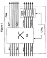
- FIG. 1 an optical switch arrangement with synchronisation feature will be described.
- the working of the optical switch arrangement will be explained by means of a functional description of the blocks shown in Fig. 1. Based on this description, implementation of the functional blocks in Fig. 1 will be obvious to a person skilled in the art and will therefor not be described in detail. In addition, the principle working of the optical switch arrangement will be described in further detail.
- the optical switch arrangement OSA includes an optical switch OS, an optical delay device ODD and a control unit CTRL.
- the optical switch OS is realised with a transparent optical crossconnect exploiting both wavelength and space domain to route incoming optical signals from optical inputs IN1, ..., INn, INn+1, ..., INn+m to optical outputs OUT1, ..., OUTn, OUTn+1, ..., OUTn+m and generates outgoing optical signals.
- the incoming optical signals as well as the outgoing optical signals and the delayed optical signals can be multiplexed or not, e.g. in the wavelength domain, which grants the optical nodes including such an optical switch arrangement a high level of transparency to acommodate a wide range of digital signals with different frame formats, coding shemes or bitrates.
- the optical switch arrangement OSA can be preceeded or followed by additional multiplexers, demultiplexers or wavelengthconverters to convert the optical signals for additional flexibility in configuring the optical network.
- the optical delay device ODD includes optical delay units ODU1, ..., ODUm which are coupled to a respective optical output of a subset of the optical outputs OUTn+1, ..., OUTn+m of the optical switch OS to delay outgoing optical signals with a predetermined delay time to generate delayed optical signals and which will be explained more in detail in further paragraphs.
- the control unit is coupled to the optical switch OS and the optical delay device ODD to control the routing and the predetermined delay time in respons of control data (not shown) provided by the network management and/or created locally.
- An incoming optical signal provided at one of the optical inputs IN1, ..., INn, INn+1, ..., INn+m is routed trough the optical switch OS to either an an optical output OUT1, ..., OUTn which is not connected to one of the optical delay units or to an optical output OUTn+1, ..., OUTn+m which is connected to one of the optical delay units and delayed with the predetermined delay time.
- the optical delay device ODD enables, the optical switch arrangement OSA to synchronise incoming optical signals and to provide synchronised outgoing optical signals. Indeed, leading incoming optical signals are, according to the previous paragraph, routed to the optical delay device ODD and delayed with a predetermined delay time which is such that the delayed optical signals are provided at the outputs of the optical delay device ODD at the same time as lagging incoming optical signals which arrive at the arrangement and are routed directly to one of the optical outputs OUT1, ..., OUTn of the optical switch OS.
- optical delay units ODU1, ..., ODUm included in the optical delay device ODD can be realised as described above in different ways.
- the optical delay units ODU1, ..., ODUm are realised advantageously according to this embodiment, by making the predetermined delay time of each delay unit also a multiple of that predetermined time interval. Part of such a modular network is shown in fiure 4 and described in the following paragraphs.
- the multiple of that predetermined time interval is respected by including in the optical delay units ODU1, ..., ODUm an optical fiber line with a fiber line length equal to a multiple of a predetermined fiber line length (to avoid overloading the figure the fiber lines are not shown).
- This predetermined fiber line length corresponds to the fiber line length of an optical fiber line which is such that the transport delay of an optical signal transmitted over this fiber line equals the above predetermined time interval.
- an incoming wavelength multiplexed optical signal of which all wavelength channels needs to be delayed by the same multiple of that predetermined time interval can be routed directly, i.e. without wavelength multiplexing or demultiplexing, through the optical switch to the optical delay device, giving at the output the wavelength multiplexed optical signal with the required delay.
- no multiplexing / demultiplexing is needed and the same fiber delay lines are used to delay all wavelength channels.
- the order of magnitude of the predetermined time interval can for instance be chosen as 125 microsec. which corresponds, take into account that optical signals travelling trough an optical fiber have the speed of 200000km / sec, with a predetermined fiber line length of about 25 km.
- Inaccuracies due to e.g. influence of the temperature on the optical fiber which gives an inaccuracy of the order of magnitude of a few picosec. or the delay trough the optical switch which gives an inaccuracy of the order of magnitude of about 10 nanosec. or a fault of e.g. 1 m at installation of the modular network which gives an inaccuracy of the order of magnitude of about 5 nanosec, are not detrimental to the working of the subject arrangement.
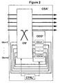
- FIG. 2 a second embodiment of an optical switch arrangement with synchronisation feature OSA' will be described. Due to simularity with the above first embodiment and taken into account that the functionality of ODD', ODU1', ODUm', CTRL', OS', INn+1'and INn+m' shown in Fig. 2 corresponds with the functionality of ODD, ODU1, ODUm, CTRL, OS, INn+1 and INn+m respectively of Fig.1, the working of the second embodiment of the optical switch arrangement OSA' can be explained by means of a functional description of the blocks shown in Fig. 1 which can be found in the previous paragraphs. Based on this description, implementation of the functional blocks in Fig. 2 will be obvious to a person skilled in the art.
- OSA' of figure 2 includes the coupling back of the optical delay units ODU1',..., ODUm' to the optical inputs INn+1', ..., INn+m' of the optical switch OSA'.
- the optical signals can be routed repetitively trough the optical switch to the optical delay device ODD' to realise the necessary delay time. It will be obvious for a person skilled in the art that a more intensive use of the optical delay units is possible and that in this way a lot of optical fiber line is saved.
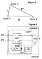
- FIG.3 an optical hitless protection switching module OHPSW wil be described wherein an optical switch arrangement OSA'' according to the present invention is used.
- OHPSW optical switch arrangement
- FIG.3 the block scheme of figure 4 is used, OHPSW being part of node B and similar modules being used in the other nodes.
- a very simple network is chosen. Obviously the invention is not restricted to this simple network.
- optical hitless protection switching module OHPSM will be explained by means of a functional description of the blocks shown in figures 3 and 4. Based on this description, implementation of the functional blocks in figures 3 and 4 will be obvious to a person skilled in the art. In addition, the principle working of the optical hitless protection switching module OHPSM will be described in further detail.
- the network of figure 4 includes three optical nodes : node A as a source node, node B as a destination node and node C.
- the length of the links between the nodes is chosen that the transfer delay of an optical signal over each link between two optical nodes is a multiple of a predetermined time interval T : between node A and node B the delay is two times T, between node A and node C the delay is one time T and between node B and node C the delay is two times T.
- Node A sends an optical signal called leading optical signal over an active path directly to node B and sends at the same time the identical optical signal called lagging optical signal over an active back-up path via node C to node B.
- the optical hitless protection switching module OHPSW of figure 4 which is included in node B includes an optical switch arrangement OSA" and an optical selector SEL.
- optical switch arrangement OSA is realised with the second embodiment as described in figure 2 taken into account that the functionality of OS", ODD", ODU” and CTRL” shown in figure 4 corresponds with the functionality of OS', ODD', ODU' and CTRL' of figure 2.
- the optical delay device ODD includes optical delay units wherefor the predetermined delay time is a multiple of the predetermined time interval T.
- the figure shows only one optical delay unit ODU" wherefor in this particular situation the predetermined delay time equals one time the predetermined time interval T.
- the optical selector SEL is coupled to the optical outputs of the optical switch arrangement OSA" and to the optical control unit CTRL''.
- the optical selector SEL selects under control of the control unit CTRL" one out of two synchronised optical signals provided by the optical switch arrangement OSA''.
- the leading optical signal arrives one time T earlier than the lagging optical signal at the optical switch arrangement OSA".
- the optical switch arrangement synchronises both signals by routing the leading optical signal to an optical output coupled to the optical delay unit ODU", delaying it with the predetermined delay time which is one time T and routing it to an optical output which is not coupled to the optical delay unit and by routing the lagging optical signal directly to an optical output which is not coupled to the optical delay unit.
- the leading and lagging optical signals which include identical information, are thus synchronised and provided to the optical selector SEL.
- the optical selector SEL selects the optical signal which came over the active path directly from node A to node B and in case of failure of this link e.g.
- the selector will switch directly to the selection of the optical signal which came over the active back-up path without losing any information.
- How the control unit is informed of the status of the links is a well known network management matter which is not part of the invention, and is therfor not described in detail.
- the present invention is also suited for use in an optical protection switching module.
- an optical hitless protection switching module OHPSW as described in the above paragraphs accompanying figures 3 and 4, is that the optical switch arrangement OSA'' is not using the ability to synchronise the identical incoming optical signals.
Landscapes
- Engineering & Computer Science (AREA)
- Computer Networks & Wireless Communication (AREA)
- Optical Communication System (AREA)
- Use Of Switch Circuits For Exchanges And Methods Of Control Of Multiplex Exchanges (AREA)
- Data Exchanges In Wide-Area Networks (AREA)
Claims (11)
- Optische Schaltanordnung (OSA) zur Aufnahme in einen optischen Knoten eines optischen Netzwerks, die einen optischen Schalter (OS) mit optischen Eingängen (IN1, ..., INn, INn+1, ..., INn+m) und optischen Ausgängen (OUT1, ..., OUTn, OUTn+1, ..., OUTn+m) enthält, wobei der optische Schalter (OS) so angepasst ist, dass er eintreffende optische Signale von den optischen Eingängen (IN1, ..., INn, INn+1, ..., INn+m) zu den optischen Ausgängen (OUT1, ..., OUTn, OUTn+1, ..., OUTn+m) leitet und dadurch abgehende optische Signale erzeugt, wobei die optische Schaltanordnung (OSA) zusätzlich folgendes enthält:Die optische Schaltanordnung (OSA) wird dadurch in die Lage versetzt, die eintreffenden optischen Signale zu synchronisieren und synchronisierte abgehende optische Signale zu erzeugen, wobei jedes der synchronisierten abgehenden optischen Signale einem entsprechenden der eintreffenden optischen Signale zugeordnet ist und abhängig von der Leitweglenkung des entsprechenden eintreffenden optischen Signals entweder durch ein entsprechendes der abgehenden optischen Signale gebildet wird, die an den optischen Ausgängen außerhalb der Untermenge der optischen Ausgänge (OUT1, ..., OUTn) bereitgestellt werden, oder durch ein entsprechendes der verzögerten optischen Signale gebildet wird, dadurch gekennzeichnet, dasseine optische Verzögerungseinrichtung (ODD), die mit dem optischen Schalter (OS) verbunden ist und verzögerte optische Signale erzeugt, wobei die optische Verzögerungseinrichtung (ODD) optische Verzögerungseinheiten (ODU1, ..., ODUm) enthält, wobei jede der optischen Verzögerungseinheiten (ODU1, ..., ODUm) mit einem entsprechenden optischen Ausgang von mindestens einer Untermenge der optischen Ausgänge (OUTn+1, ..., OUTn+m) verbunden und so angepasst ist, dass er ein abgehendes optisches Signal der abgehenden optischen Signale, die an dem entsprechenden Ausgang bereitgestellt werden, um eine vordefinierte Verzögerungszeit verzögert und dadurch eines der verzögerten optischen Signale erzeugt;eine Steuereinheit (CTRL), die mit dem optischen Schalter (OS) und mit der optischen Verzögerungseinrichtung (ODD) verbunden ist, um die Weiterleitung, bzw. die vordefinierte Verzögerungszeit zu steuern;
die vordefinierte Verzögerungszeit ein ganzzahliges Vielfaches eines vordefinierten Zeitintervalls (T) ist und dass das optische Netzwerk optische Verbindungen zwischen seinen optischen Knoten umfasst, wofür die Laufzeit der optischen Signale ein Vielfaches des vordefinierten Zeitintervalls ist. - Die optische Schaltanordnung (OSA) gemäß Anspruch 1, dadurch gekennzeichnet, dass mindestens ein Teil der optischen Verzögerungseinheiten (ODU1, ..., ODUm) zu einem der optischen Eingänge (INn+1, ..., INn+m) zurück gekoppelt ist.
- Die optische Schaltanordnung (OSA) gemäß Anspruch 1, dadurch gekennzeichnet, dass jede der optischen Verzögerungseinheiten (ODU1, ..., ODUm) eine optische Faserstrecke enthält, deren Länge ein ganzzahliges Vielfaches einer vordefinierten Faserlänge ist und dass die vordefinierte Faserlänge durch die Länge einer Faserstrecke definiert ist, die so ist, dass die Laufzeit eines optischen Signals über die Faserstrecke gleich dem vordefinierten Zeitintervall (T) ist.
- Die optische Schaltanordnung gemäß Anspruch 1, dadurch gekennzeichnet, dass die optische Schaltanordnung weiterhin einen optischen Selektor enthält, der so angepasst ist, dass er gesteuert durch eine zweite Steuereinheit eines aus einer Vielzahl von abgehenden optischen Signalen oder aus den verzögerten optischen Signalen auswählt und dadurch ein ausgewähltes optisches Signal erzeugt, wobei die Vielzahl der abgehenden optischen Signale oder der verzögerten optischen Signale einer Vielzahl von identischen eintreffenden optischen Signalen entspricht.
- Die optische Schaltanordnung (OHPSW) gemäß Anspruch 1, dadurch gekennzeichnet, dass die optische Schaltanordnung weiterhin einen optischen Selektor (SEL) enthält, der so angepasst ist, dass er gesteuert durch eine zweite Steuereinheit eines aus der Vielzahl synchronisierter abgehender optischer Signale, die durch die optische Schaltanordnung (OHPSW) erzeugt werden, auswählt, und dadurch ein ausgewähltes optisches Signal erzeugt, wobei die Vielzahl synchronisierter abgehender optischer Signale einer Vielzahl identischer eintreffender optischer Signale entspricht.
- Optisches Netzwerk mit optischen Knoten, dadurch gekennzeichnet, dass mindestens ein optischer Knoten der optischen Knoten mindestens eine optische Schaltanordnung (OSA) gemäß einem der Ansprüche 1 bis 5 enthält, und dass das optische Netzwerk optische Verbindungen zwischen seinen optischen Knoten enthält, wobei die Laufzeit der optischen Signale ein Vielfaches des vordefinierten Zeitintervalls ist.
- Ein optisches Schaltverfahren zum Einsatz in einem optischen Knoten eines optischen Netzwerks, das folgende Schritte umfasst:Leitweglenkung der eintreffenden optischen Signale von optischen Eingängen (IN1, ..., INn, INn+1, ..., INn+m) zu optischen Ausgängen (OUT1, ..., OUTn, OUTn+1, ..., OUTn+m) eines optischen Schalters (OS) und dadurch Erzeugung abgehender optischer Signale; undVerzögerung mindestens einer Untermenge der abgehenden optischen Signale um vordefinierte Verzögerungszeiten, um verzögerte optische Signale zu erhalten; undSynchronisation der eintreffenden optischen Signale durch Steuerung der Leitweglenkung und der vordefinierten Verzögerungszeiten und dadurch Erzeugung synchronisierter abgehender optischer Signale, wobei jedes der synchronisierten abgehenden optischen Signale einem entsprechenden der eintreffenden optischen Signale zugeordnet ist und abhängig von der Leitweglenkung des entsprechenden eintreffenden optischen Signals entweder durch ein entsprechendes der abgehenden optischen Signale außerhalb der Untermenge der abgehenden optischen Signale oder durch ein entsprechendes der verzögerten optischen Signale gebildet wird, was von der Leitweglenkung des entsprechenden eintreffenden optischen Signals abhängt, dadurch gekennzeichnet, dass das optische Schaltverfahren die Definition der vordefinierten Verzögerungszeiten als ganzzahliges Vielfaches eines vordefinierten Zeitintervalls (T) umfasst, und wobei das optische Netzwerk optische Verbindungen zwischen seinen optischen Knoten enthält, für welche die Laufzeit der optischen Signale ein Vielfaches des vordefinierten Zeitintervalls ist.
- Ein optisches Schaltverfahren gemäß Anspruch 7, dadurch gekennzeichnet, dass das optische Schaltverfahren zusätzlich einen Schritt der Rückkopplung mindestens eines Teils der verzögerten optischen Signale auf einen der optischen Eingänge (INn+1, ..., INn+m) umfasst.
- Ein optisches Schaltverfahren gemäß Anspruch 7, dadurch gekennzeichnet, dass der Schritt der Verzögerung mindestens einer Untermenge der abgehenden optischen Signale um die vordefinierten Verzögerungszeiten durch optische Faserstrecken realisiert wird, wobei die Faserlänge ein ganzzahliges Vielfaches einer vordefinierten Faserlänge ist und die vordefinierte Faserlänge durch die Faserlänge einer optischen Faserstrecke definiert ist, die so ist, dass die Laufzeit eines optischen Signals über die Faserstrecke gleich dem vordefinierten Zeitintervall (T) ist.
- Das optische Schaltverfahren gemäß Anspruch 7, dadurch gekennzeichnet, dass es weiterhin einen Schritt der Auswahl einer Vielzahl von abgehenden optischen Signalen oder der verzögerten optischen Signale umfasst, die einer Vielzahl von identischen eintreffenden optischen Signalen entsprechen.
- Das optische Schaltverfahren gemäß Anspruch 7, dadurch gekennzeichnet, dass es weiterhin einen Schritt der Auswahl einer Vielzahl von synchronisierten abgehenden optischen Signalen umfasst, die einer Vielzahl von identischen eintreffenden optischen Signalen entsprechen.
Priority Applications (4)
| Application Number | Priority Date | Filing Date | Title |
|---|---|---|---|
| DE69634769T DE69634769T2 (de) | 1996-02-16 | 1996-02-16 | Optischer Schalter mit Synchronisation |
| EP96200406A EP0790750B1 (de) | 1996-02-16 | 1996-02-16 | Optischer Schalter mit Synchronisation |
| AU12535/97A AU725007B2 (en) | 1996-02-16 | 1997-02-07 | An optical switch arrangement |
| US08/800,878 US5978120A (en) | 1996-02-16 | 1997-02-14 | Optical switch arrangement with synchronisation feature and in particular optical protection switching module and optical hitless protection switching module using such an arrangement and methods realized by such arrangement and modules |
Applications Claiming Priority (1)
| Application Number | Priority Date | Filing Date | Title |
|---|---|---|---|
| EP96200406A EP0790750B1 (de) | 1996-02-16 | 1996-02-16 | Optischer Schalter mit Synchronisation |
Publications (2)
| Publication Number | Publication Date |
|---|---|
| EP0790750A1 EP0790750A1 (de) | 1997-08-20 |
| EP0790750B1 true EP0790750B1 (de) | 2005-05-25 |
Family
ID=8223688
Family Applications (1)
| Application Number | Title | Priority Date | Filing Date |
|---|---|---|---|
| EP96200406A Expired - Lifetime EP0790750B1 (de) | 1996-02-16 | 1996-02-16 | Optischer Schalter mit Synchronisation |
Country Status (4)
| Country | Link |
|---|---|
| US (1) | US5978120A (de) |
| EP (1) | EP0790750B1 (de) |
| AU (1) | AU725007B2 (de) |
| DE (1) | DE69634769T2 (de) |
Families Citing this family (14)
| Publication number | Priority date | Publication date | Assignee | Title |
|---|---|---|---|---|
| US6839514B1 (en) * | 1999-09-29 | 2005-01-04 | Ciena Corporation | Method and apparatus for operation, protection, and restoration of heterogeneous optical communication networks |
| US6137608A (en) * | 1998-01-30 | 2000-10-24 | Lucent Technologies Inc. | Optical network switching system |
| JP3248573B2 (ja) * | 1998-08-13 | 2002-01-21 | 日本電気株式会社 | 光遅延装置および光遅延方法 |
| US6529301B1 (en) * | 1999-07-29 | 2003-03-04 | Nortel Networks Limited | Optical switch and protocols for use therewith |
| US7463581B1 (en) | 2000-02-07 | 2008-12-09 | Cisco Technology, Inc. | Re-routing connections using redundant path connections and loopbacks |
| JP2001268011A (ja) * | 2000-03-21 | 2001-09-28 | Fujitsu Ltd | 光ノードシステム、及び、スイッチの接続方法 |
| FR2819665B1 (fr) | 2001-01-15 | 2003-04-11 | Cit Alcatel | Dispositif de commutation photonique |
| US6798946B2 (en) | 2001-12-14 | 2004-09-28 | Molex Incorporated | Method to deskew parallel optical links |
| US20030175028A1 (en) * | 2002-03-13 | 2003-09-18 | Kapil Shrikhande | Method and apparatus for hitlessly accessing a data signal using a signaling protocol |
| JP4638754B2 (ja) * | 2005-03-18 | 2011-02-23 | 富士通株式会社 | 光装置および光クロスコネクト装置 |
| FR2897491B1 (fr) * | 2006-02-16 | 2008-05-09 | Alcatel Sa | Dispositif de combinaison/recombinaison de bits pour la protection de trafic dans un noeud d'un reseau de communication |
| CN101989906B (zh) | 2009-07-30 | 2013-12-18 | 华为技术有限公司 | 报文同步方法、装置及系统 |
| US10382158B2 (en) | 2013-10-03 | 2019-08-13 | The Hong Kong Polytechnic University | Reversible wavelength channels for optical communication networks |
| US20150098477A1 (en) * | 2013-10-03 | 2015-04-09 | Versitech Limited | Reversible wavelength channels for optical communication networks |
Family Cites Families (11)
| Publication number | Priority date | Publication date | Assignee | Title |
|---|---|---|---|---|
| FR2672172B1 (fr) * | 1991-01-29 | 1993-06-04 | Cit Alcatel | Matrice de commutation photonique. |
| GB9104861D0 (en) * | 1991-03-07 | 1991-04-17 | Univ Strathclyde | Communications switching network |
| DE69232305T2 (de) * | 1991-12-16 | 2002-07-25 | AT & T CORP., NEW YORK | Optische Paketvermittlungstelle |
| US5285441A (en) * | 1992-03-17 | 1994-02-08 | At&T Bell Laboratories | Errorless line protection switching in asynchronous transer mode (ATM) communications systems |
| DE4315545A1 (de) * | 1992-05-15 | 1993-11-18 | Siemens Ag | Ein- oder mehrstufige ATM-Koppelanordnung mit einem zwischen zwei Raumkoppelvielfachen liegenden Zwischenspeicher in jeder Stufe |
| EP0569901B1 (de) * | 1992-05-15 | 2002-09-25 | Siemens Aktiengesellschaft | Optische Koppeleinrichtung |
| EP0637879A1 (de) * | 1993-04-16 | 1995-02-08 | Nec Corporation | Störungsfreie Umschaltungsanordnung und Verfahren für ein optisches Netz |
| US5416769A (en) * | 1993-07-13 | 1995-05-16 | At&T Corp. | Controlled-feedback packet switching system |
| DE4332841A1 (de) * | 1993-09-27 | 1995-03-30 | Siemens Ag | Anordnung zur Verzögerung eines optischen Signals |
| US5402256A (en) * | 1994-03-31 | 1995-03-28 | At&T Corp. | Optical time slot interchanger apparatus and method of operation |
| FR2726726A1 (fr) * | 1994-11-04 | 1996-05-10 | Guillemot Christian | Systeme de commutateur pour paquets optiques |
-
1996
- 1996-02-16 EP EP96200406A patent/EP0790750B1/de not_active Expired - Lifetime
- 1996-02-16 DE DE69634769T patent/DE69634769T2/de not_active Expired - Fee Related
-
1997
- 1997-02-07 AU AU12535/97A patent/AU725007B2/en not_active Ceased
- 1997-02-14 US US08/800,878 patent/US5978120A/en not_active Expired - Lifetime
Also Published As
| Publication number | Publication date |
|---|---|
| US5978120A (en) | 1999-11-02 |
| AU1253597A (en) | 1997-08-21 |
| AU725007B2 (en) | 2000-10-05 |
| DE69634769D1 (de) | 2005-06-30 |
| DE69634769T2 (de) | 2006-03-23 |
| EP0790750A1 (de) | 1997-08-20 |
Similar Documents
| Publication | Publication Date | Title |
|---|---|---|
| US6226111B1 (en) | Inter-ring cross-connect for survivable multi-wavelength optical communication networks | |
| CA2164778C (en) | Ring network communication structure on an optical carrier and reconfigurable node for said structure | |
| JP2989269B2 (ja) | 光ネットワーク用交差接続 | |
| EP0790750B1 (de) | Optischer Schalter mit Synchronisation | |
| US5712932A (en) | Dynamically reconfigurable WDM optical communication systems with optical routing systems | |
| CA2254606C (en) | Ring network for sharing protection resource by working communication paths | |
| Hunter et al. | Approaches to optical Internet packet switching | |
| US6344912B1 (en) | Hybrid and scalable opto-electronic processing in a wavelength-division multiplexed system | |
| EP0726691A2 (de) | Kombinierter Wellenlängenrouter und Vermittlungseinrichtung für ein optisches Wellenlängenmultiplex-Kommunikationssystem | |
| US20040190901A1 (en) | Bi-directional optical network element and its control protocols for WDM rings | |
| WO1995033324A2 (en) | Optical telecommunications network | |
| US6061482A (en) | Channel layered optical cross-connect restoration system | |
| EP1323255B1 (de) | Optischer vermittlungsrouter | |
| KR20040033202A (ko) | 다파장 광 교환 시스템 | |
| JP4408806B2 (ja) | Wdmネットワークのためのパス保護の方法及びそれに応じたノード | |
| US20010038475A1 (en) | Synchronous digital communications system | |
| US6738579B2 (en) | Synchronous digital communications system | |
| US6690891B1 (en) | Method for synchronizing optical signals, an optical synchronizing devices and an optical network node therefor | |
| EP1422966B1 (de) | Wellenlängenumwandler und optisches Querverbindungssystem mit Verwendung derselben | |
| WO1999018679A1 (en) | An optical network with protection path for failure recovery | |
| EP1352542B1 (de) | Optischer schalter | |
| US6714341B1 (en) | Wavelength converter and optical cross-connect system using the same | |
| KR100281419B1 (ko) | 완전광 패킷 스위칭 시스템 | |
| CHOI et al. | A photonic ATM switch architecture for WDM optical networks | |
| EP1195940A1 (de) | Verfahren zur synchronisierung optischer signalen, optische synchronisationsanordnungen und zugehöriger optischer netzknoten |
Legal Events
| Date | Code | Title | Description |
|---|---|---|---|
| PUAI | Public reference made under article 153(3) epc to a published international application that has entered the european phase |
Free format text: ORIGINAL CODE: 0009012 |
|
| AK | Designated contracting states |
Kind code of ref document: A1 Designated state(s): BE DE ES FR GB IT |
|
| 17P | Request for examination filed |
Effective date: 19980220 |
|
| 17Q | First examination report despatched |
Effective date: 20031202 |
|
| GRAP | Despatch of communication of intention to grant a patent |
Free format text: ORIGINAL CODE: EPIDOSNIGR1 |
|
| RAP1 | Party data changed (applicant data changed or rights of an application transferred) |
Owner name: ALCATEL |
|
| GRAS | Grant fee paid |
Free format text: ORIGINAL CODE: EPIDOSNIGR3 |
|
| GRAA | (expected) grant |
Free format text: ORIGINAL CODE: 0009210 |
|
| AK | Designated contracting states |
Kind code of ref document: B1 Designated state(s): BE DE ES FR GB IT |
|
| PG25 | Lapsed in a contracting state [announced via postgrant information from national office to epo] |
Ref country code: BE Free format text: LAPSE BECAUSE OF FAILURE TO SUBMIT A TRANSLATION OF THE DESCRIPTION OR TO PAY THE FEE WITHIN THE PRESCRIBED TIME-LIMIT Effective date: 20050525 |
|
| REG | Reference to a national code |
Ref country code: GB Ref legal event code: FG4D |
|
| REF | Corresponds to: |
Ref document number: 69634769 Country of ref document: DE Date of ref document: 20050630 Kind code of ref document: P |
|
| PG25 | Lapsed in a contracting state [announced via postgrant information from national office to epo] |
Ref country code: ES Free format text: LAPSE BECAUSE OF FAILURE TO SUBMIT A TRANSLATION OF THE DESCRIPTION OR TO PAY THE FEE WITHIN THE PRESCRIBED TIME-LIMIT Effective date: 20050905 |
|
| PGFP | Annual fee paid to national office [announced via postgrant information from national office to epo] |
Ref country code: IT Payment date: 20060228 Year of fee payment: 11 |
|
| ET | Fr: translation filed | ||
| PLBE | No opposition filed within time limit |
Free format text: ORIGINAL CODE: 0009261 |
|
| STAA | Information on the status of an ep patent application or granted ep patent |
Free format text: STATUS: NO OPPOSITION FILED WITHIN TIME LIMIT |
|
| 26N | No opposition filed |
Effective date: 20060228 |
|
| PGFP | Annual fee paid to national office [announced via postgrant information from national office to epo] |
Ref country code: GB Payment date: 20070216 Year of fee payment: 12 Ref country code: DE Payment date: 20070216 Year of fee payment: 12 |
|
| PGFP | Annual fee paid to national office [announced via postgrant information from national office to epo] |
Ref country code: FR Payment date: 20070212 Year of fee payment: 12 |
|
| GBPC | Gb: european patent ceased through non-payment of renewal fee |
Effective date: 20080216 |
|
| REG | Reference to a national code |
Ref country code: FR Ref legal event code: ST Effective date: 20081031 |
|
| PG25 | Lapsed in a contracting state [announced via postgrant information from national office to epo] |
Ref country code: DE Free format text: LAPSE BECAUSE OF NON-PAYMENT OF DUE FEES Effective date: 20080902 |
|
| PG25 | Lapsed in a contracting state [announced via postgrant information from national office to epo] |
Ref country code: FR Free format text: LAPSE BECAUSE OF NON-PAYMENT OF DUE FEES Effective date: 20080229 |
|
| PG25 | Lapsed in a contracting state [announced via postgrant information from national office to epo] |
Ref country code: GB Free format text: LAPSE BECAUSE OF NON-PAYMENT OF DUE FEES Effective date: 20080216 |
|
| PG25 | Lapsed in a contracting state [announced via postgrant information from national office to epo] |
Ref country code: IT Free format text: LAPSE BECAUSE OF NON-PAYMENT OF DUE FEES Effective date: 20070216 |