EP0789297B1 - Data processor loading data and performing multiply-add operation in parallel - Google Patents
Data processor loading data and performing multiply-add operation in parallel Download PDFInfo
- Publication number
- EP0789297B1 EP0789297B1 EP96119559A EP96119559A EP0789297B1 EP 0789297 B1 EP0789297 B1 EP 0789297B1 EP 96119559 A EP96119559 A EP 96119559A EP 96119559 A EP96119559 A EP 96119559A EP 0789297 B1 EP0789297 B1 EP 0789297B1
- Authority
- EP
- European Patent Office
- Prior art keywords
- data
- instruction
- register
- unit
- value
- Prior art date
- Legal status (The legal status is an assumption and is not a legal conclusion. Google has not performed a legal analysis and makes no representation as to the accuracy of the status listed.)
- Expired - Lifetime
Links
- 230000015654 memory Effects 0.000 claims abstract description 74
- 238000012546 transfer Methods 0.000 claims description 35
- 238000012545 processing Methods 0.000 description 95
- 238000007792 addition Methods 0.000 description 27
- 238000010586 diagram Methods 0.000 description 14
- 238000006073 displacement reaction Methods 0.000 description 13
- 230000004044 response Effects 0.000 description 12
- 238000004364 calculation method Methods 0.000 description 10
- 230000006870 function Effects 0.000 description 9
- 238000000034 method Methods 0.000 description 8
- 101150043159 Rsrc1 gene Proteins 0.000 description 6
- 101150099915 Rsrc2 gene Proteins 0.000 description 6
- 238000013507 mapping Methods 0.000 description 6
- 238000010276 construction Methods 0.000 description 5
- 238000012805 post-processing Methods 0.000 description 3
- 230000008569 process Effects 0.000 description 3
- 238000001514 detection method Methods 0.000 description 2
- 238000007726 management method Methods 0.000 description 2
- 230000001343 mnemonic effect Effects 0.000 description 2
- 230000004048 modification Effects 0.000 description 2
- 238000012986 modification Methods 0.000 description 2
- 230000001186 cumulative effect Effects 0.000 description 1
- 238000013523 data management Methods 0.000 description 1
- 230000001419 dependent effect Effects 0.000 description 1
- 230000006872 improvement Effects 0.000 description 1
Images


Classifications
-
- G—PHYSICS
- G06—COMPUTING; CALCULATING OR COUNTING
- G06F—ELECTRIC DIGITAL DATA PROCESSING
- G06F9/00—Arrangements for program control, e.g. control units
- G06F9/06—Arrangements for program control, e.g. control units using stored programs, i.e. using an internal store of processing equipment to receive or retain programs
- G06F9/30—Arrangements for executing machine instructions, e.g. instruction decode
- G06F9/38—Concurrent instruction execution, e.g. pipeline, look ahead
- G06F9/3885—Concurrent instruction execution, e.g. pipeline, look ahead using a plurality of independent parallel functional units
- G06F9/3893—Concurrent instruction execution, e.g. pipeline, look ahead using a plurality of independent parallel functional units controlled in tandem, e.g. multiplier-accumulator
-
- G—PHYSICS
- G06—COMPUTING; CALCULATING OR COUNTING
- G06F—ELECTRIC DIGITAL DATA PROCESSING
- G06F9/00—Arrangements for program control, e.g. control units
- G06F9/06—Arrangements for program control, e.g. control units using stored programs, i.e. using an internal store of processing equipment to receive or retain programs
- G06F9/30—Arrangements for executing machine instructions, e.g. instruction decode
- G06F9/30003—Arrangements for executing specific machine instructions
- G06F9/30007—Arrangements for executing specific machine instructions to perform operations on data operands
- G06F9/3001—Arithmetic instructions
- G06F9/30014—Arithmetic instructions with variable precision
-
- G—PHYSICS
- G06—COMPUTING; CALCULATING OR COUNTING
- G06F—ELECTRIC DIGITAL DATA PROCESSING
- G06F9/00—Arrangements for program control, e.g. control units
- G06F9/06—Arrangements for program control, e.g. control units using stored programs, i.e. using an internal store of processing equipment to receive or retain programs
- G06F9/30—Arrangements for executing machine instructions, e.g. instruction decode
- G06F9/30003—Arrangements for executing specific machine instructions
- G06F9/30072—Arrangements for executing specific machine instructions to perform conditional operations, e.g. using predicates or guards
-
- G—PHYSICS
- G06—COMPUTING; CALCULATING OR COUNTING
- G06F—ELECTRIC DIGITAL DATA PROCESSING
- G06F9/00—Arrangements for program control, e.g. control units
- G06F9/06—Arrangements for program control, e.g. control units using stored programs, i.e. using an internal store of processing equipment to receive or retain programs
- G06F9/30—Arrangements for executing machine instructions, e.g. instruction decode
- G06F9/30145—Instruction analysis, e.g. decoding, instruction word fields
- G06F9/30149—Instruction analysis, e.g. decoding, instruction word fields of variable length instructions
-
- G—PHYSICS
- G06—COMPUTING; CALCULATING OR COUNTING
- G06F—ELECTRIC DIGITAL DATA PROCESSING
- G06F9/00—Arrangements for program control, e.g. control units
- G06F9/06—Arrangements for program control, e.g. control units using stored programs, i.e. using an internal store of processing equipment to receive or retain programs
- G06F9/30—Arrangements for executing machine instructions, e.g. instruction decode
- G06F9/30145—Instruction analysis, e.g. decoding, instruction word fields
- G06F9/3016—Decoding the operand specifier, e.g. specifier format
- G06F9/30167—Decoding the operand specifier, e.g. specifier format of immediate specifier, e.g. constants
-
- G—PHYSICS
- G06—COMPUTING; CALCULATING OR COUNTING
- G06F—ELECTRIC DIGITAL DATA PROCESSING
- G06F9/00—Arrangements for program control, e.g. control units
- G06F9/06—Arrangements for program control, e.g. control units using stored programs, i.e. using an internal store of processing equipment to receive or retain programs
- G06F9/30—Arrangements for executing machine instructions, e.g. instruction decode
- G06F9/3017—Runtime instruction translation, e.g. macros
- G06F9/30178—Runtime instruction translation, e.g. macros of compressed or encrypted instructions
-
- G—PHYSICS
- G06—COMPUTING; CALCULATING OR COUNTING
- G06F—ELECTRIC DIGITAL DATA PROCESSING
- G06F9/00—Arrangements for program control, e.g. control units
- G06F9/06—Arrangements for program control, e.g. control units using stored programs, i.e. using an internal store of processing equipment to receive or retain programs
- G06F9/30—Arrangements for executing machine instructions, e.g. instruction decode
- G06F9/32—Address formation of the next instruction, e.g. by incrementing the instruction counter
- G06F9/322—Address formation of the next instruction, e.g. by incrementing the instruction counter for non-sequential address
- G06F9/325—Address formation of the next instruction, e.g. by incrementing the instruction counter for non-sequential address for loops, e.g. loop detection or loop counter
-
- G—PHYSICS
- G06—COMPUTING; CALCULATING OR COUNTING
- G06F—ELECTRIC DIGITAL DATA PROCESSING
- G06F9/00—Arrangements for program control, e.g. control units
- G06F9/06—Arrangements for program control, e.g. control units using stored programs, i.e. using an internal store of processing equipment to receive or retain programs
- G06F9/30—Arrangements for executing machine instructions, e.g. instruction decode
- G06F9/34—Addressing or accessing the instruction operand or the result ; Formation of operand address; Addressing modes
- G06F9/355—Indexed addressing
- G06F9/3552—Indexed addressing using wraparound, e.g. modulo or circular addressing
-
- G—PHYSICS
- G06—COMPUTING; CALCULATING OR COUNTING
- G06F—ELECTRIC DIGITAL DATA PROCESSING
- G06F9/00—Arrangements for program control, e.g. control units
- G06F9/06—Arrangements for program control, e.g. control units using stored programs, i.e. using an internal store of processing equipment to receive or retain programs
- G06F9/30—Arrangements for executing machine instructions, e.g. instruction decode
- G06F9/38—Concurrent instruction execution, e.g. pipeline, look ahead
- G06F9/3818—Decoding for concurrent execution
- G06F9/3822—Parallel decoding, e.g. parallel decode units
-
- G—PHYSICS
- G06—COMPUTING; CALCULATING OR COUNTING
- G06F—ELECTRIC DIGITAL DATA PROCESSING
- G06F9/00—Arrangements for program control, e.g. control units
- G06F9/06—Arrangements for program control, e.g. control units using stored programs, i.e. using an internal store of processing equipment to receive or retain programs
- G06F9/30—Arrangements for executing machine instructions, e.g. instruction decode
- G06F9/38—Concurrent instruction execution, e.g. pipeline, look ahead
- G06F9/3836—Instruction issuing, e.g. dynamic instruction scheduling or out of order instruction execution
- G06F9/3853—Instruction issuing, e.g. dynamic instruction scheduling or out of order instruction execution of compound instructions
-
- G—PHYSICS
- G06—COMPUTING; CALCULATING OR COUNTING
- G06F—ELECTRIC DIGITAL DATA PROCESSING
- G06F9/00—Arrangements for program control, e.g. control units
- G06F9/06—Arrangements for program control, e.g. control units using stored programs, i.e. using an internal store of processing equipment to receive or retain programs
- G06F9/30—Arrangements for executing machine instructions, e.g. instruction decode
- G06F9/38—Concurrent instruction execution, e.g. pipeline, look ahead
- G06F9/3885—Concurrent instruction execution, e.g. pipeline, look ahead using a plurality of independent parallel functional units
- G06F9/3889—Concurrent instruction execution, e.g. pipeline, look ahead using a plurality of independent parallel functional units controlled by multiple instructions, e.g. MIMD, decoupled access or execute
Landscapes
- Engineering & Computer Science (AREA)
- Software Systems (AREA)
- Theoretical Computer Science (AREA)
- Physics & Mathematics (AREA)
- General Physics & Mathematics (AREA)
- General Engineering & Computer Science (AREA)
- Computational Mathematics (AREA)
- Mathematical Analysis (AREA)
- Mathematical Optimization (AREA)
- Pure & Applied Mathematics (AREA)
- Advance Control (AREA)
- Executing Machine-Instructions (AREA)
Abstract
Description
- The present invention relates to a data processor for high-speed digital signal processing and a method of processing data for high-speed digital signal processing.
- Digital signal processors (DSPs) having an architecture suitable for signal processing have been used as data processors designed specifically for high-speed digital signal processing. These DSPs execute processing frequently used in signal processing such as a multiply-add operation at high speeds. An example of the DSPs is Motorola DSP56000. The DSP56000 comprises two address pointers, two data memories, and a multiply-add operation unit. Parallel execution of the load of data (e.g., the load of coefficients and data) from two 1-word memories specified respectively by the address pointers, the update of the two address pointers, and the multiply-add operation allows the multiply-add operation to be executed with a high throughput (DSP56000 Digital Signal Processor Family Manual, 1992). In this manner, the DSP normally has two memories. Data are distributed to either of the memories. Some DSPs use a 2-port RAM for efficient data transfer.
- An example of microprocessors incorporating the DSP function includes Motorola CPU16. The CPU16 may repeatedly perform the multiply-add operation and 2-word load in response to one RMAC instruction. However, the CPU16 wherein one multiply-add operation requires 12 cycles is difficult to achieve the performance competing with the DSPs (CPU16 Reference Manual, 1993).
- In recent years, some microprocessors have been intended for implementing signal processing by means of software as the operating frequency improves. To improve the arithmetic performance, some of the microprocessors additionally provide the multiply-add operation instructions and make the most of sophisticated parallel processing techniques such as superpipeline and superscalar to achieve DSP-level performance. For example, PowerPC603 (Motorola and IBM) may execute a single-precision floating-point multiply-add operation with one clock cycle throughput by using 3-stage pipeline processing. This requires the amount of hardware and significantly complicated control. To perform one multiply-add operation for each clock cycle, one clock cycle requires 2-word data. The PowerPC603 may load a maximum of one word for each clock cycle, resulting in an insufficient supply of operands (Proceedings of COMPCON 1994: "The PowerPC603 Microprocessor: A High Performance, Low Power, Superscalar RISC Microprocessor", PowerPC603 RISC Microprocessor User's Manual, 1994).
- The DSPs which must include two memories have a complicated memory construction and require very cumbersome data management for distribution of data between the two memories. The use of a 2-port RAM adds to the area and costs of the data processor. Additionally, the DSP is in general an accumulator machine and is difficult to execute complicated data processing.
- The microprocessors which require one memory have a relatively simple memory construction. However, the microprocessors are not efficient in signal processing unlike the DSPs wherein hardware directly represents the flow of signal processing. To achieve the DSP-level performance, the state-of-the-art microprocessors require an increased amount of hardware, adding to the costs of the data processor. Further, the microprocessors are difficult to reduce power consumption because of the need for operation at high frequencies.
- NAKAJIMA M. ET AL: 'Ohmega: a VLSI superscalar processor architecture for numerical applications' COMPUTER ARCHITECTURE NEWS, vol. 19, no. 3, May 1991, US, pages 160-168, discloses a data processor comprising an instruction memory for storing instructions including a first operation code and a second operation code, a data memory, an instruction decode unit for decoding the first and second operation codes in parallel, a register file, several operation units for performing an arithmetic operation and an operand access unit operated in parallel with the operation unit.
- According to the present invention as set out in
claim 1, a data processor comprises: a first memory portion for storing an instruction including a first operation code and a second operation code; a second memory portion for storing data; an instruction decode unit for receiving the instruction stored in the first memory portion, the instruction decode unit including first and second decoders for decoding the first and second operation codes in parallel, respectively; a register file portion including a plurality of registers for storing data to transfer data from and to the second memory portion; an operation unit for receiving first data stored in a first register of the register file portion to perform an arithmetic operation using the first data in response to a control signal, the control signal being the first operation code decoded by the first decoder of the instruction decode unit; and an operand access unit operated in parallel with the operation unit for causing second and third data stored in the second memory portion to be transferred in parallel and stored in second and third registers of the register file portion, respectively, in response to a control signal, the control signal being the second operation code decoded by the second decoder of the instruction decode unit. - According to the present invention, the second and third data each are n bit (n is a natural number) in length, and the second and third data are combined together into 2n-bit data when the second and third data are transferred to the register file portion.
- According to the present invention, the operation unit includes a multiplier for multiplying together the first data and fourth data stored in a fourth register of the register file portion, and an adder for adding at least two data together, the adder adding together the result of multiplication of the multiplier and data stored in a register of the register file portion to cause a register of the register file portion to store the result of addition.
- It is therefore an object of the present invention to provide an inexpensive high-performance microprocessor-type data processor which readily reduces power consumption under relatively simple control.
- It is another object of the present invention to provide a data processor having DSP-level digital signal processing performance.
- It is still another object of the present invention to provide a method of processing data which may achieve high-performance data processing control.
- These and other objects, features, aspects and advantages of the present invention will become more apparent from the following detailed description of the present invention when taken in conjunction with the accompanying drawings.
-
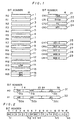
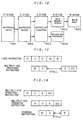
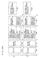
- Fig. 1 illustrates a set of registers for a data processor according to a first preferred embodiment of the present invention;
- Fig. 2 illustrates a processor status word for the data processor according to the first preferred embodiment of the present invention;
- Fig. 3 illustrates an instruction format for the data processor according to the first preferred embodiment of the present invention;
- Fig. 4 illustrates a short format of a 2-operand instruction for the data processor according to the first preferred embodiment of the present invention;
- Fig. 5 illustrates a short format of a branch instruction for the data processor according to the first preferred embodiment of the present invention;
- Fig. 6 illustrates a long format of a 3-operand instruction or a load/store instruction for the data processor according to the first preferred embodiment of the present invention;
- Fig. 7 illustrates a format of an instruction having an operation code in its left-hand container for the data processor according to the first preferred embodiment of the present invention;
- Fig. 8 is a functional block diagram of the data processor according to the first preferred embodiment of the present invention;
- Fig. 9 is a detailed block diagram of a first operation unit for the data processor according to the first preferred embodiment of the present invention;
- Fig. 10 is a detailed block diagram of a PC unit for the data processor according to the first preferred embodiment of the present invention;
- Fig. 11 is a detailed block diagram of a second operation unit for the data processor according to the first preferred embodiment of the present invention;
- Fig. 12 illustrates pipeline processing for the data processor according to the first preferred embodiment of the present invention;
- Fig. 13 illustrates a pipeline state when a load operand interference occurs in the data processor according to the first preferred embodiment of the present invention;
- Fig. 14 illustrates a pipeline state when an arithmetic hardware interference occurs in the data processor according to the first preferred embodiment of the present invention;
- Fig. 15 illustrates a program of a 256 tap FIR filter for the data processor according to the first preferred embodiment of the present invention;
- Fig. 16 illustrates a bit pattern when a 2-word load instruction and a multiply-add operation instruction are executed in parallel in the data processor according to the first preferred embodiment of the present invention;
- Fig. 17 illustrates the contents of an internal instruction memory corresponding to a loop part of the program of the FIR filter for the data processor according to the first preferred embodiment of the present invention;
- Fig. 18 illustrates mapping of an internal data memory in relation to coefficients and data in the program of the FIR filter for the data processor according to the first preferred embodiment of the present invention;
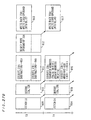
- Fig. 19 shows respective positions of Figs. 19A to 19C;
- Figs. 19A to 19C illustrate a flow of processing in a loop of the program of the FIR filter for the data processor according to the first preferred embodiment of the present invention;
- Fig. 20 illustrates signal lines of an n-stage secondary direct-form type-II IIR filter;
- Fig. 21 illustrates a program of the IIR filter for the data processor according to the first preferred embodiment of the present invention;
- Fig. 22 illustrates the contents of the internal instruction memory corresponding to a loop part of the program of the IIR filter for the data processor according to the first preferred embodiment of the present invention;
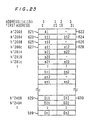
- Fig. 23 illustrates mapping of the internal data memory in relation to coefficients and data in the program of the IIR filter for the data processor according to the first preferred embodiment of the present invention;
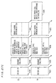
- Fig. 24 shows respective positions of Figs. 24A to 24C;
- Figs. 24A to 24C illustrate a flow of processing in a loop of the program of the IIR filter for the data processor according to the first preferred embodiment of the present invention;
- Fig. 25 illustrates a loop part of a program of an IFFT for the data processor according to the first preferred embodiment of the present invention;
- Fig. 26 illustrates a loop part of a program of a subtract-absolute-add operation for the data processor according to the first preferred embodiment of the present invention;
- Fig. 27 shows respective positions of Figs. 27A to 27C;
- Figs. 27A to 27C illustrate a flow of processing in the loop of the program of the ubtract-absolute-add operation for the data processor according to the first preferred embodiment of the present invention;
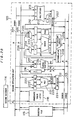
- Fig. 28 is a detailed block diagram of the second operation unit for the data processor according to a second preferred embodiment of the present invention;
- Fig. 29 illustrates a program of a subtract-square-add operation for the data processor according to the second preferred embodiment of the present invention;
- Fig. 30 illustrates the contents of the internal instruction memory corresponding to a loop part of the program of the subtract-square-add operation for the data processor according to the second preferred embodiment of the present invention;
- Fig. 31 illustrates mapping of the internal data memory in relation to data in the program of the subtract-square-add operation for the data processor according to the second preferred embodiment of the present invention;
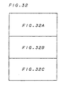
- Fig. 32 shows respective positions of Figs. 32A to 32C;
- Figs. 32A to 32C illustrate a flow of processing in the loop of the program of the subtract-square-add operation for the data processor according to the second preferred embodiment of the present invention;
- Fig. 33 illustrates the contents of the internal instruction memory corresponding to the loop part of the program of the subtract-absolute-add operation for the data processor according to the second preferred embodiment of the present invention;
- Fig. 34 shows respective positions of Figs. 34A to 34C;
- Figs. 34A to 34C illustrate a flow of processing in the loop of the program of the subtract-absolute-add operation for the data processor according to the second preferred embodiment of the present invention;
- Fig. 35 is a functional block diagram of the data processor according to a third preferred embodiment of the present invention;
- Fig. 36 illustrates an instruction format for the data processor according to the third preferred embodiment of the present invention;
- Fig. 37 is a block diagram of the second operation unit for the data processor according to a fourth preferred embodiment of the present invention;
- Fig. 38 illustrates an instruction format for the data processor according to the fourth preferred embodiment of the present invention;
- Fig. 39 illustrates a basic format of containers of an instruction for the data processor according to the fourth preferred embodiment of the present invention; and
- Fig. 40 illustrates a loop part of the program of the FIR filter for the data processor according to the fourth preferred embodiment of the present invention.
-
- A data processor according to a first preferred embodiment of the present invention will be described below. The data processor of the first preferred embodiment is a 16-bit processor whose addresses and data are 16 bits in length.
- Fig. 1 illustrates a set of registers for the data processor of this preferred embodiment. The data processor employs big endian bit and byte ordering wherein the most significant bit is the
bit 0. - Sixteen general-purpose registers R0 to R15 are provided for storing data and address values therein. The general-purpose registers R0 to R14 are designated by the
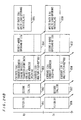
numerals 1 to 15 in Fig. 1, respectively. The general-purpose register R13 (designated at 14 in Fig. 1) is allocated as a link (LINK) register for storing a return address for a subroutine jump. The general-purpose register R15 is a register for a stack pointer (SP) including an interruption stack pointer (SPI) 16 and a user stack pointer (SPU) 17. A processor status word (PSW) to be described later switches between the interruption stack pointer (SPI) 16 and the user stack pointer (SPU) 17. TheSPI 16 and theSPU 17 are generically referred to as an SP hereinafter. The number of each of the registers is specified in a 4-bit register specification field unless otherwise specified. The data processor of this preferred embodiment includes an instruction for processing a pair of registers, e.g. R0 and R1. In this case, the pair of registers are specified in such a manner that an even-numbered register is specified thereby to indirectly specify the corresponding register having the odd number which equals the even number plus one. - The reference numerals 21 to 29 designate 16-bit control registers. The number of each of the control registers is represented by 4 bits, similar to those of the general-purpose registers. The control register CR0 designated at 21 is a register for the processor status word (PSW) including a bit for specifying the operating mode of the data processor and a flag indicative of the result of operations. Fig. 2 illustrates the construction of the
PSW 21. Thereference numeral 41 designates an SM bit (bit 0) indicative of a stack mode for specifying the corresponding relationship when the general-purpose register R15 is specified as above described. TheSM bit 41 indicates an interruption mode when it is "0". Then, the SPI is used as the general-purpose register R15. TheSM bit 41 indicates a user mode when it is "1". Then, the SPU is used as the general purpose-register R15. Thereference numeral 42 designates an IE bit (bit 5) for specifying an interruption enable state. When the IE bit is "0", the interruption is masked (ignored if asserted). When the IE bit is "1", the interruption is accepted. A repeat function for achieving zero-overhead loop processing is implemented in the data processor of this preferred embodiment. Thereference numeral 43 designates an RP bit (bit 6) indicative of a repeat state. The RP bit indicates no repeat being executed when it is "0". The RP bit indicates a repeat being executed when it is "1". A modulo addressing function which is addressing for accessing a circular buffer is implemented in the data processor of this preferred embodiment. Thereference numeral 44 designates an MD bit (bit 7) for specifying a modulo enable state. When the MD bit is "0", the modulo addressing is disabled. When the MD bit is "1", the modulo addressing is enabled. Thereference numeral 45 designates an execution control flag (bit 12) to which the result of a comparison instruction or the like is set. Thereference numeral 46 designates a carry flag (bit 15) to which a carry is set when addition and subtraction instructions are executed. - The control register CR2 designated at 23 in Fig. 1 is a register for a program counter (PC) indicative of the instruction address being executed. The length of the instruction processed by the data processor of this preferred embodiment is basically fixed at 32 bits. The
program counter 23 holds a word address wherein 32 bits make up one word. - The control register CR1 designated at 22 in Fig. 1 is a register for a backup processor status word (BPSW), and the control register CR3 designated at 24 in Fig. 1 is a register for a backup program counter (BPC). The control registers CR1 and CR3 are registers for saving and holding the values of the
PSW 21 andPC 23 being executed if an exception or an interruption is detected, respectively. - The control registers 25 to 27 are repeat-associated registers which allow a user to read and write the values thereof so that an interruption is accepted during a repeat. The control register CR7 designated at 25 in Fig. 1 is a register for a repeat counter (RPT_C) for holding the count value indicative of the subsequent repeat count. The control register CR8 designated at 26 in Fig. 1 is a register for a repeat start address (RPT_S) for holding the first instruction address in the block to be repeated. The control register CR9 designated at 27 in Fig. 1 is a register for a repeat end address (RPT_E) for holding the last instruction address in the block to be repeated.
- The control registers 28 and 29 are provided to execute modulo addressing. The control register CR10 designated at 28 in Fig. 1 holds a modulo start address (MOD_S), and the control register CR11 designated at 29 in Fig. 1 holds a modulo end address (MOD_E). Both of the control registers CR10 and CR11 hold the first and last word (16 bits) addresses. When the modulo addressing is used during an increment, the lower address is set to the
MOD_S 28, and the higher address is set to theMOD_E 29. If the initial value held in the register to be incremented coincides with the address held in theMOD_E 29, the value held in theMOD_S 28 is written back to the register as an incremented result. - The reference numerals 31 and 32 designate 40-bit accumulators A0 and A1 for holding the result of a multiply-add operation in an integer format. The accumulators A0 and A1 designated at 31 and 32 in Fig. 1 comprise areas A0H (31b) and A1H (32b) for holding the high-
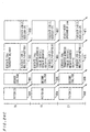
order 16 bits of the result of the multiply-add operation, areas A0L (31c) and A1L (32c) for holding the low-order 16 bits of the result of the multiply-add operation, and 8 guard bit areas A0G (31a) and A1G (32a) for holding bits overflown out of the high order bit of the result of the multiply-add operation, respectively. - The data processor of the first preferred embodiment processes a 2-way VLIW (very long instruction word) instruction set. Fig. 3 illustrates an instruction format for the data processor of the first preferred embodiment. The length of the instruction is basically fixed at 32 bits, and the instruction is aligned in 4-byte (32-bit) boundary. Each 32-bit instruction code comprises 2 format specification bits (FM bits) 51 indicative of the format of the instruction, a 15-bit left-
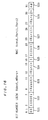
hand container 52, and a 15-bit right-hand container 53. Each of thecontainers containers - The
FM bits 51 may specify the format of the instruction and the order of two short instructions to be executed. If theFM bits 51 are "11", theFM bits 51 indicate that thecontainers FM bits 51 indicate that each of thecontainers FM bits 51 specify the order of execution. If theFM bits 51 are "00", theFM bits 51 indicate that two short instructions are executed in parallel. If they are "01", theFM bits 51 indicate that the short instruction held in the right-hand container 53 is executed after the short instruction held in the left-hand container 52 is executed. If they are "10", theFM bits 51 indicate that the short instruction held in the left-hand container 52 is executed after the short instruction held in the right-hand container 53 is executed. In this manner, the first preferred embodiment allows encoding into one 32-bit instruction including two short instructions to be executed sequentially, improving encoding efficiency. - Figs. 4 to 7 illustrate typical instruction encoding; Fig. 4 shows the instruction encoding of a short instruction having two operands.
Fields field 64 specifies an accumulator number in some cases.Fields field 63 specifies a 4-bit short immediate value in some cases. Fig. 5 shows the instruction encoding of a short-format branch instruction including anoperation code field 71 and an 8-bitbranch displacement field 72. The branch displacement is specified by offset of a word (32 bits) offset, like the PC value. Fig. 6 shows a format of a 3-operand instruction having a 16-bit displacement or immediate value or a load/store instruction which includes anoperation code field 81, fields 82 and 83 for specifying a register number like the short format, and anextended data field 84 for specifying the 16-bit displacement or immediate value. Fig. 7 shows a format of an instruction having an operation code in its right-hand container 53 wherein a 2-bit field 91 indicates "01". The reference numerals 93 and 96 designate operation code fields, and 94 and 95 designate fields for specifying a register number or the like. Thereference numeral 92 designates reserved bits used for the operation code or register number as required. - Further, there are provided some operations having special instruction encoding, for example, an instruction wherein all 15 bits constitutes an operation code such as an NOP (no operation) instruction, and a one-operand instruction.
- Sub-instructions for the data processor of this preferred embodiment are a RISC-like instruction set. Only the load/store instruction directs that the memory data are accessed, and the operation instruction directs that an arithmetic operation is performed on an operand in the register/accumulator or an immediate operand. There are five operand data addressing modes: a register indirect mode, a register indirect mode with post-increment, a register indirect mode with post-decrement, a push mode, and a register relative indirect mode whose mnemonics are "@Rsrc", "@Rsrc+", "@Rsrc-", "@-SP", "@(disp16, Rsrc)", respectively, where Rsrc is a register number for specifying a base address, and disp16 is the 16-bit displacement value. The address of the operand is specified by a byte address.
- All of the modes except the register relative indirect mode have the instruction format shown in Fig. 4. The
field 63 specifies a base register number, and thefield 62 specifies the number of a register into which a value loaded from the memory is written or the number of a register for holding the value to be stored. In the register indirect mode, the value of the register specified as the base register serves as the operand address. In the register indirect mode with post-decrement, the value of the register specified as the base register serves as the operand address, and the value in the base register is post-incremented by the size (the number of bytes) of the operand and written back. In the register indirect mode with post-decrement, the value of the register specified as the base register serves as the operand address, and the value in the base register is post-decremented by the size (the number of bytes) of the operand and written back. The push mode is usable only when the store instruction is provided and the base register is the register R15. In the push mode, the stack pointer (SP) value pre-decremented by the size (the number of bytes) of the operand serves as the operand address, and the decremented value is written back to the SP. - The register relative indirect mode has the instruction format shown in Fig. 6. The
field 83 specifies a base register number, and thefield 82 specifies the number of a register into which the value loaded from the memory is written or the number of a register for holding the value to be stored. Thefield 84 specifies the value of displacement of the position at which the operand is stored from the base address. In the register relative indirect mode, the 16-bit displacement value added to the value in the register specified as the base register serves as the operand address. - The post-increment type register indirect mode and the post-decrement type register indirect mode may use a modulo addressing mode by setting the
MD bit 44 in thePSW 21 to "1". - Jump target addressing of a jump instruction includes a register indirect addressing for specifying the jump target address by using a register value, and a PC relative indirect addressing for specifying the jump target address by using a branch displacement of the jump instruction from the PC. The PC relative indirect addressing includes a short format addressing for specifying the branch displacement by using 8 bits, and a long format addressing for specifying the branch displacement by using 16 bits. Further, the data processor has a repeat instruction for start of the repeat function which achieves loop processing without overhead.
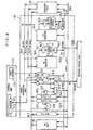
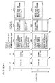
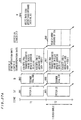
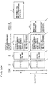
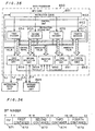
- Fig. 8 is a functional block diagram of a
data processor 100 according to the first preferred embodiment of the present invention. Thedata processor 100 comprises anMPU core 101, an instruction fetchunit 102 for accessing instruction data in response to a request from theMPU core 101, aninternal instruction memory 103, anoperand access unit 104 for accessing operand data in response to a request from theMPU core 101, aninternal data memory 105, and an externalbus interface unit 106 for arbitrating requests from the instruction fetchunit 102 andoperand access unit 104 to access a memory external of thedata processor 100. - The
MPU core 101 comprises an instruction queue 111, acontrol unit 112, aregister file 115, afirst operation unit 116, asecond operation unit 117, and aPC unit 118. - The instruction queue 111 holds 2 entries of 32-bit instruction code and a valid bit. The queue is controlled in a FIFO (first-in first-out) order. The instruction queue 111 temporarily holds instruction data fetched by the instruction fetch
unit 102 to transmit the instruction data to thecontrol unit 112. - The
control unit 112 performs entire control on theMPU core 101, for example, control of the instruction queue 111, pipeline control, execution of instructions, and interface with the instruction fetchunit 102 andoperand access unit 104. Thecontrol unit 112 comprises aninstruction decode unit 119 for decoding an instruction code transmitted from the instruction queue 111. Theinstruction decode unit 119 includes two decoders, that is, first andsecond decoders first decoder 113 decodes the instruction to be executed in thefirst operation unit 116, and thesecond decoder 114 decodes the instruction to be executed in thesecond operation unit 117. In a first cycle of decoding of a 32-bit instruction, thefirst decoder 113 analyzes an instruction code in the left-hand container 52 and thesecond decoder 114 analyzes an instruction code in the right-hand container 53. The data in theFM bits 51, and thebit 0 andbit 1 of the left-hand container 52 are analyzed by both of the first andsecond decoders hand container 53 is sent to thefirst decoder 113 to extract the extended data which is not analyzed. Thus the instruction to be executed first must be located in a position corresponding to an operation unit for executing the instruction. If two short instructions are executed in sequential order, the instruction to be executed later is transmitted to both of the first andsecond decoders second decoders first decoder 113 is validated and the decoded result in thesecond decoder 114 is invalidated. - The
register file 115 includes theregisters 1 to 17 and is connected to thefirst operation unit 116,second operation unit 117, andPC unit 118 by a plurality of buses. - Fig. 9 is a detailed block diagram of the
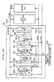
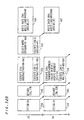
first operation unit 116. Thefirst operation unit 116 is connected to theregister file 115 by anS1 bus 301, an S2 bus 302, and anS3 bus 303 to read data from the registers through the threebuses S1 bus 301 and S2 bus 302 together may transmit 2-word data from the pair of registers in parallel. Thefirst operation unit 116 is also connected to theregister file 115 through aD1 bus 311, a W1 bus 314, and aW2 bus 315 to write data into the registers through the threebuses W2 bus 315 is connected to only the odd-numbered registers. The W1 bus 314 andW2 bus 315 together may transmit 2-word data to the pair of registers in parallel. - An
AA latch 151 and anAB latch 152 are input latches for anALU 153. TheAA latch 151 receives a register value read through theS1 bus 301 orS3 bus 303 and has a zero clear function. TheAB latch 152 receives a register value read through theS3 bus 303 or a 16-bit immediate value generated by decoding in thefirst decoder 113, and has a zero clear function. TheALU 153 mainly performs transfer, comparison, arithmetic and logic operation, calculation/transfer of operand addresses, increment/decrement of the base address values of the operand addresses, and calculation/transfer of the jump target addresses. The results of operation and address modification are written back to the register specified by the instruction in theregister file 115 through aselector 155 and theD1 bus 311. An AO latch 154 is a latch for holding operand addresses, and selectively holds and outputs the result of address calculation in theALU 153 or the base address value held in theAA latch 151 to theoperand access unit 104 through anOA bus 321. For calculation or transfer of the jump target address, the output from theALU 153 is transferred to thePC unit 118 through aJA bus 323. - An
MOD_S 156 and anMOD_E 157 are control registers corresponding to the control registers CR10 (28) and CR11 (29) of Fig. 1, respectively. Acomparator 158 compares the value in theMOD_E 157 with the base address value on theS3 bus 303. With the modulo addressing enabled in the register indirect mode with post-increment/decrement, the value in theMOD_S 156 which is held in thelatch 159 is written back to the base address register in theregister file 115 through theselector 155 and theD1 bus 311. - A store data (SD) register 160 includes two 16-bit registers and temporarily holds store data outputted to the
S1 bus 301 or to both of theS1 bus 301 and S2 bus 302. Data held in the SD register 160 are transferred to analignment circuit 162 through alatch 161. Thealignment circuit 162 aligns the data into 32-bit form in accordance with the operand address to output the data to theoperand access unit 104 through alatch 163 and anOD bus 322. - The data loaded by the
operand access unit 104 are applied to a load data (LD) register 164 including two 16-bit registers through theOD bus 322. The value in theLD register 164 is transferred to analignment circuit 166 through alatch 165. Thealignment circuit 166 aligns the data to output data to be transferred to the even-numbered registers to the W1 bus 314 and data to be transferred to the odd-numbered registers to theW2 bus 315. When 1-word data are loaded, load data are outputted to one of the W1 bus 314 and theW2 bus 315. When 2-word data are loaded, the load data are outputted to both of the W1 bus 314 and theW2 bus 315. The outputted data are written into the specified register in theregister file 115. - A
PSW 171 in thecontrol unit 112 is a register for holding the value in the control register CR0 (21) of Fig. 1. APSW updating unit 172 including a latch updates the value in thePSW 171 in response to the result of an operation or by the execution of an instruction. To transfer a value to thePSW 171, only assigned bits are transferred from theAB latch 152 to thecontrol unit 112. To read a value from thePSW 171, the value is outputted from thePSW updating unit 172 to theD1 bus 311 and is written to theregister file 115. ABPSW 167 is a register corresponding to the control register CR1 (22) of Fig. 1. During exception processing, the value in thePSW 21 outputted to theD1 bus 311 is written to theBPSW 167. The value in theBPSW 167 is read to theS3 bus 303 and transferred to thePSW 171 or theregister file 115. - Fig. 10 is a detailed block diagram of the
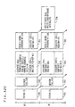
PC unit 118. An instruction address (IA)register 181 holds the address of the instruction to be fetched next and outputs the address of the instruction to be fetched to the instruction fetchunit 102. When the subsequent instruction is to be fetched, the address value transferred from the IA register 181 through alatch 182 is incremented by 1 in anincrementor 183 and then written back to theIA register 181. If the sequence is changed by a jump or repeat, the IA register 181 receives the jump target address transferred by theJA bus 323. - An
RPT_S 184, anRPT_E 186, and anRPT_C 188 are repeat control registers and correspond to the control registers CR8 (26), CR9 (27), and CR7 (25) in the register set of Fig. 1, respectively. TheRPT_E 186 holds the address of the last instruction in the block to be repeated. The last address is calculated in thefirst operation unit 116 during repeat instruction processing and applied to theRPT_E 186 through theJA bus 323. Acomparator 187 compares the value of the end address in the repeat block held in theRPT_E 186 with the value of a fetch address held in theIA register 181. If the value in theRPT_C 188 for holding a repeat count is not "1" during repeat processing and the two addresses coincide with each other, a start address of the block to be repeated which is held in theRPT_S 184 is transferred to the IA register 181 through alatch 185 and theJA bus 323. Each time the instruction at the last address of the block to be repeated is executed, the value in theRPT_C 188 is decremented by 1 by adecrementor 190 through alatch 189. If the result of decrement equals zero, theRP bit 43 in thePSW 21 is cleared and the repeat processing is terminated. TheRPT_S 184,RPT_E 186, andRPT_C 188 have an input port from theD1 bus 311 and an output port to theS3 bus 303. By using these buses, initialization caused by repeat instruction processing as well as saving and return operations are performed. - An execution stage PC (EPC) 194 holds the PC value of the instruction being executed, and a next instruction PC (NPC) 191 calculates the PC value of the instruction to be executed next. If a jump occurs during execution, the
NPC 191 receives the value on theJA bus 323 to which the jump target address is transferred. If a branch occurs during a repeat, theNPC 191 receives the first address in the block to be repeated from thelatch 185. In other cases, the value in theNPC 191 transferred through alatch 192 is incremented by anincrementor 193 and then written back to theNPC 191. In the case of a subroutine jump instruction, the value in thelatch 192 is outputted as a return address to theD1 bus 311 and then written back to the register R13 defined as the link register in theregister file 115. If the next instruction is to be placed into execution, the value in thelatch 192 is transferred to theEPC 194. If the PC value of the instruction being executed is to be referred to, the value in theEPC 194 is outputted to theS3 bus 303 and transferred to thefirst operation unit 116. ABPC 196 corresponds to the control register CR3 (23) in the register set of Fig. 1. If an exception or interruption is detected, the value in theEPC 194 is transferred to theBPC 196 through alatch 195. TheBPC 196 has an input port from theD1 bus 311 and an output port to theS3 bus 303, and transfer to/from theregister file 115 is performed. - Fig. 11 is a detailed block diagram of the
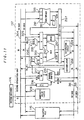
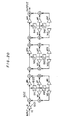
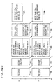
second operation unit 117. Thesecond operation unit 117 is connected to theregister file 115 by anS4 bus 304 and anS5 bus 305 to read data from the registers through the twobuses S4 bus 304 andS5 bus 305 together may transfer 2-word data from the pair of registers in parallel. Thesecond operation unit 117 is also connected to theregister file 115 by aD2 bus 312 and aD3 bus 313 to write data into the registers through the twobuses D2 bus 312 is connected to all registers, but theD3 bus 313 is connected to only the odd-numbered registers. TheD2 bus 312 andD3 bus 313 together may transfer 2-word data to the pair of registers in parallel. -
Accumulators 208 correspond to the two 40-bit accumulators A0 and A designated at 31 and 32 of Fig. 1. - The
reference numeral 201 designates a 40-bit ALU including a guard bit adder for the accumulator which is 8 bits long (bit 0 to bit 7), an arithmetic and logic unit which is 16 bits long (bit 8 to bit 23), and an adder for adding the low-order 16 bits of the accumulator which is 16 bits long (bit 24 to bit 39). TheALU 201 performs addition and subtraction of up to 40 bits and a logic operation of 16 bits. - An
A latch 202 and aB latch 203 are input latches for theALU 201. TheA latch 202 receives the data on theS4 bus 304 at thebit 8 to bit 23 positions, receives the value in theaccumulator 208 intactly through ashifter 204, or receives the value in theaccumulator 208 arithmetically 16 bits right-shifted through theshifter 204. Ashifter 205 receives the value in theaccumulator 208 through an interconnecting line 206 (8 guard bits), the S4 bus 304 (high-order 16 bits) and the S5 bus 305 (low-order 16 bits) or receives the value in the register subjected to sign extension into 40 bits through only theS5 bus 305 or through the S4 andS5 buses shifter 205 receives the value arithmetically shifted by any amount ranging from 3 bits left-shift to 1 bit right-shift. TheB latch 203 receives the data on theS5 bus 305 at thebit 8 to bit 23 positions or receives the output from amultiplier 211 through theP latch 214 or the output from theshifter 205. TheA latch 202 andB latch 203 have the function to clear the data therein to zero and to set the data therein to a constant value. - If a destination operand indicates the
accumulator 208, the output from theALU 201 is written into theaccumulator 208 through aselector 207. If the designation operand indicates the register, the output from theALU 201 is written into theregister file 115 through theselector 207 and either theD2 bus 312 only (1-word data) or both of theD2 bus 312 and D3 bus 313 (2-word data). Asaturation circuit 209 receives the output from theALU 201 and has the function of clipping its output to a maximum or minimum value expressible as 16 bits or 32 bits with reference to the guard bits to output data containing high-order 16 bits or both high-order and low-order 32 bits. The output from thesaturation circuit 209 may be written into theregister file 115 through only the D2 bus 312 (1-word data) or through both of theD2 bus 312 and D3 bus 313 (2-word data). For calculation of absolute values and execution of maximum and minimum value setting instructions, the outputs of theA latch 202 and theB latch 203 are connected to the input of theselector 207. - A priority encoder (PENC) 210 receives the value in the
B latch 203. The PENC generates the shift count value required to normalize the input data in a fixed-point format and outputs the result to theregister file 115 through theD2 bus 312. - An
X latch 212 and aY latch 213 receive 16-bit values on theS4 bus 304 andS5 bus 305, respectively, and have the function of zero extension or sign extension of the 16-bit values to 17 bits. - The
multiplier 211 is a 17-bit × 17-bit multiplier for multiplying the value stored in theX latch 212 by the value stored in theY latch 213. If themultiplier 211 receives a multiply-add instruction or a multiply-subtract instruction, the result of multiplication is applied to aP latch 214 and transmitted to theB latch 203. If themultiplier 211 receives a multiply instruction and the destination operand indicates theaccumulator 208, the result of multiplication is written into theaccumulator 208 through theselector 207. - A
barrel shifter 215 may perform an up-to-16-bits left and right arithmetic/logic shift on 40-bit or 16-bit data. A shift data (SD)latch 217 receives as shift data the value in theaccumulator 208 or the value in the register applied through theS4 bus 304. A shift count (SC)latch 216 receives as a shift count the immediate value or the register value through theS5 bus 305. Thebarrel shifter 215 performs a shift specified by the operation code on the data in theSD latch 217 by the shift count specified by theSC latch 216. The result of shift is written back to theaccumulator 208 or to the register file through theD2 bus 312. Theshifter 215 has a 2-word transfer function. Specifically, theshifter 215 outputs the 2-word data received through theS4 bus 304 andS5 bus 305 to theD2 bus 312 andD3 bus 313 through theSD latch 217 andshifter 215 to write back the 2-word data into theregister file 115. Theshifter 215 may perform 1-word transfer. - An
immediate value latch 218 extends a 6-bit immediate value generated by thesecond decoder 114 into a 16-bit value and then holds the 16-bit value to transfer the 16-bit value to an arithmetic unit through theS5 bus 305. - Pipeline processing in the data processor will be described below according to the first preferred embodiment of the present invention. Fig. 12 illustrates the pipeline processing. The data processor of the first preferred embodiment performs 5-stage pipeline processing including an instruction fetch (IF)
stage 401 for fetching instruction data, an instruction decode (D)stage 402 for analyzing instructions; an instruction execution stage (E) 403 for executing operations; a memory access (M)stage 404 for accessing a data memory, and a write back (W)stage 405 for writing operands loaded from a memory into a register. For multiply-add/multiply-subtract operations, further 2-stage pipeline including multiplication and addition is used to execute instructions. The latter stage processing is referred to as an instruction execution 2 (E2)stage 406. - At the
IF stage 401, a fetch of instructions, management of the instruction queue 111, and repeat control are mainly performed. TheIF stage 401 controls the operations of the instruction fetchunit 102, theinternal instruction memory 103, the externalbus interface unit 106, the instruction queue 111, the IA register 181,latch 182,incrementor 182 andcomparator 187 in thePC unit 118, and units for performing the stage control, the instruction fetch control, control ofPC unit 118 and control of theinstruction queue 11 in thecontrol unit 113. TheIF stage 401 is initialized by a jump at theE stage 403. - The fetch address is held in the
IA register 181. If a jump occurs at theE stage 403, the IA register 181 receives the jump target address through theJA bus 323 to perform initialization. When the instruction data are fetched sequentially, theincrementor 182 increments the address. The sequence switching control is performed if thecomparator 187 detects a coincidence between the value in the IA register 181 and the value in theRPT_E 186 during repeat processing and the value in theRPT_C 188 is not "1". Then, the value held in theRPT_S 184 is transferred to the IA register 181 through thelatch 185 andJA bus 323. - The value in the IA register 181 is sent to the instruction fetch
unit 102 which in turn fetches the instruction data. If the corresponding instruction data are stored in theinternal instruction memory 103, an instruction code is read from theinternal instruction memory 103. In this case, the instruction fetch is completed within one clock cycle. If the corresponding instruction data are not stored in theinternal instruction memory 103, an instruction fetch request is sent to the externalbus interface unit 106. The externalbus interface unit 106 arbitrates between the instruction fetch request and a request form theoperand access unit 104. When the externalbus interface unit 106 accepts the instruction fetch request from the instruction fetchunit 102, the externalbus interface unit 106 reads out the instruction data from an external memory, and transmits the fetched instruction to the instruction fetchunit 102. The externalbus interface unit 106 requires a minimum of 2 clock cycles to access the external memory. The instruction fetchunit 102 transfers the received instruction to the instruction queue 111. The instruction queue 111 is a 2-entry queue and outputs the instruction code received under FIFO control to theinstruction decoders - At the
D stage 402, theinstruction decode unit 119 analyzes operation code and generates execution control signals to control thefirst operation unit 116, thesecond operation unit 117, and thePC unit 188 to execute instructions. TheD stage 402 is initialized by a jump at theE stage 403. If the instruction code sent from the instruction queue 111 is invalid, theD stage 402 is placed in an idle cycle and waits for an valid instruction code to be received. If theE stage 403 is not permitted to start the next processing, the execution control signals are invalidated, and theD stage 403 waits for the termination of processing of the preceding instruction at theE stage 403. For example, such a condition occurs when the instruction being executed at theE stage 403 is a memory access instruction and the preceding memory access is not terminated at theM stage 404. - The
D stage 402 also performs division of two instructions to be sequentially executed, sequence control of a 2-cycle execution instruction, a conflict check on a load operand using a scoreboard register (not shown), and a conflict check on a operation unit in thesecond operation unit 117. If these conflicts are detected, the output of the control signal is inhibited until the conflict is cancelled. Fig. 13 illustrates an example of the load operand conflict. If immediately after a load instruction a multiply-add operation instruction refers to an operand to be loaded by the load instruction, the start of execution of the multiply-add operation instruction is inhibited until the load to the register is completed. In this case, a 2-clock-cycle stall occurs if the memory access is terminated within one clock cycle. Fig. 14 illustrates an example of an hardware resourcee conflict on the second operation. If a rounding instruction which uses an adder is immediately after a multiply-add operation instruction, the start of execution of the rounding instruction is inhibited until the operation of the preceding instruction is terminated. In this case, a 1-clock-cycle stall occurs. No stalls occur if the multiply-add operation instructions are executed successively. - The
first decoder 113 mainly generates operation control signals for entire control of thefirst operation unit 116, control of parts of thePC unit 118 which are not controlled by theIF stage 401, read control of theregister file 115 to theS1 bus 301, S2 bus 302, andS3 bus 303, and write control thereof from theD1 bus 311. Thefirst decoder 113 also generates the instruction-dependent control information to be used in theM stage 404 andW stage 405 and this information is sent through the pipeline. Thesecond decoder 114 mainly generates execution control signals in thesecond operation unit 117. - The
E stage 403 performs processing of almost all instruction executions except the memory access and addition of the multiply-add/multiply-subtract operation instructions, such as an arithmetic operation, comparison, data transfer between registers including control registers, operand address calculation of the load/store instructions, calculation of the jump target address of the jump instruction, jump processing, EIT (exception, interruption, trap) detection, and jump to an EIT vector table. - With interruption enabled, the interruption is detected at the end of a 32-bit instruction without fail. No interruption is accepted between two short instructions to be sequentially executed in the 32-bit instruction.
- The completion of the execution at the
E stage 403 must be in a wait condition when the instruction being processed at theE stage 403 is an operand access instruction and a preceding memory access at theM stage 404 is not completed. Stage control is performed in thecontrol unit 112. - At the
E stage 403, thefirst operation unit 116 performs arithmetic and logic operations, comparison, and transfer. TheALU 153 calculates the address of the memory operand including modulo control and a branch target address. - The value in the register specified as the operand by an instruction is transferred to the
first operation unit 116. Extended data such as an immediate and displacement value are also transferred from thefirst decoder 113 if necessary. Arithmetic and logical operation is performed inALU 153 and the result is written back to theregister file 115 through theD1 bus 311. If the load/store instruction is provided, the result of the arithmetic operation is transmitted to theoperand access unit 104 through the AO latch 154 andOA bus 321. If the jump instruction is provided, the jump target address is transmitted to the respective units through theJA bus 323. The store data are read from theregister file 115 through theS1 bus 301 and S2 bus 302 and are held and aligned. Then, the store data are transferred to theoperand access unit 104 through theOD bus 322. ThePC unit 118 manages the PC value of the instruction being executed and calculates the next instruction address. Data transfer between the control register (except the accumulator) and theregister file 115 is carried out by both of thefirst operation unit 116 and thePC unit 118. - At the
E stage 403, thesecond operation unit 116 executes all operations except addition of the multiply-add operation, such as arithmetic and logic operations, comparison, transfer, and shift. The value of an operand is transferred from theregister file 115,immediate value register 218, andaccumulator 208 to respective operation units through theS4 bus 304,S5 bus 305 and other exclusive paths, and is subjected to a specified operation. The result of the operation is written back to theaccumulator 208, or to theregister file 115 through theD2 bus 312 and theD3 bus 313. - The control signal generated in the
second decoder 114 for execution of the addition and subtraction of the multiply-add/multiply-subtract operation is held under control of theE stage 403. - In the
M stage 404 operand memory access is performed according to the address sent from thefirst operation unit 116. Theoperand access unit 104 reads/writes data from/to theinternal data memory 105 or an on-chip IO (not shown) in one clock cycle if the operand is in theinternal data memory 105 or the on-chip IO. Theoperand access unit 104 outputs a data access request to the externalbus interface unit 106 if the operand is not in theinternal data memory 105 or the on-chip IO (not shown). The externalbus interface unit 106 accesses data in the external memory, and transfers the read data to theoperand access unit 104 if the load instructions is provided. The externalbus interface unit 106 requires a minimum of two clock cycles to access the external memory. If the load instruction is provided, theoperand access unit 104 transfers the read data to the LD register 164 through theOD bus 322. TheM stage 404 control is performed in thecontrol unit 112. - In the W stage, alignment of loaded operands, zero/sign extension of byte data, and writing to the
register file 115 are performed. - At the
E2 stage 406, theALU 201 executes the addition and subtraction of the multiply-add/multiply-subtract operation. - The data processor of this preferred embodiment uses a clock signal generated by multiplying an input clock by four to obtain the internal clock signal. Each of the pipeline stage requires a minimum of one internal clock cycle to terminate processing thereof. The details of the clock control are not directly related to the present invention and hence are not described.
- An example of processing of the respective sub-instructions is discussed below. The processing of operation instructions such as addition, subtraction, logic operation, and comparison, and register-to-register transfer instructions is terminated in three stages: the
IF stage 401, theD stage 402, and theE stage 403. The operations and data transfer are executed at theE stage 403. - The multiply-add/multiply-subtract instruction requires 2 clock cycles for execution of multiplication at the
E stage 403 and addition and subtraction at theE2 stage 406, that is, substantially 4-stage processing. - The load instruction requires five stages: the
IF stage 401, theD stage 402, theE stage 403, theM stage 404, and theW stage 405 to terminate the processing. The store instruction requires four stages: theIF stage 401, theD stage 402, theE stage 403, and theM stage 404 to terminate the processing. - An instruction which requires 2 cycles for execution directs that the first and
second instruction decoders second instruction decoders - One long instruction performs the above described processing. Two instructions to be executed in parallel performs the above described processing in accordance with the instruction that takes more number of clock cycle to execute instruction in the
E stage 403. For example, a combination of the instruction to be executed in two cycles and the instruction to be executed in one cycle requires two cycles. Two short instructions to be executed sequentially are decoded sequentially in theD stage 402 and executed sequentially in theE stage 403. For example, two addition instructions to be terminated at theE stage 403 are divided into respective instruction processes at theD stage 402 and executed over 2 cycles at theE stage 403. - An example of processing is described below on the basis of some programs.
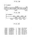
- Fig. 15 illustrates an exemplary program of a 256-tap FIR (finite impulse response) filter (frame processing) of the data processor according to the first preferred embodiment. The symbol " || " in Fig. 15 indicates that two short instructions are executed in parallel. The FIR filter executes the following calculation:where A[i] is a coefficient array and D[i] is a data array. This calculation includes 256 multiply-add operations. The coefficient and the data each are 16 bits in length.

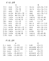
- In Fig. 15, initialization is designated at 501, loop processing at 502, and post-processing at 503. The loop processing without overhead is implemented by a repeat (repi) instruction. A block of 6 instructions between the instruction next to the repi instruction and the instruction specified by the label "loopend" is executed 42 times. The repi instruction is a long instruction including an operation code, a 16-bit displacement for specifying the last address of the repeat block in the PC relative mode, and an 8-bit immediate value for specifying the repeat count, and requires two clock cycles for execution. In the first cycle, the instruction address next to the repi instruction is transferred from the
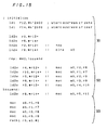
latch 192 to theRPT_S 184 and thelatch 185 through theD1 bus 311. The address of the repi instruction is transferred from theEPC 194 through theS3 bus 303 to theAA latch 151, and the displacement value specified by the instruction is applied from thefirst decoder 113 to theAB latch 152. TheALU 153 adds the data in theAA latch 151 andAB latch 152 together to transfer the result of addition which is the last instruction address of the block to be repeated to theRPT_E 186 through theJA bus 323. In the second cycle, the 8-bit immediate value which is zero-extended into 16 bits is applied from thefirst decoder 113 to theAB latch 152 and is then transferred to theRPT_C 188 through theALU 153 andD1 bus 311. TheRP bit 43 in thePSW 21 is set to "1". In this manner, initialization required for repeat processing is terminated. The registers R0 to R5 are used as a buffer for data; the registers R6 to R11 are used as a buffer for coefficients; the register R12 is used as a data pointer; and the register R14 is used as a pointer for coefficients. - The processing in the loop is described in detail hereinafter. Each instruction includes the load instruction and the multiply-add operation instruction, and the two short instructions are executed in parallel. In Fig. 15, "LD2W Rdest, @Rsrc+" indicates that 2-word (32-bit) data are fetched using the contents of the register specified by Rsrc as an operand address, and the fetched operand value is written to a pair of registers specified by Rdest (e.g., a pair of registers R0 and R1 when Rdest indicates R0). The value of Rsrc plus 4 (byte size of the operand) is written back. "MAC Adest, Rsrc1, Rsrc2" indicates the multiply-add operation instruction. The value in the register specified by Rsrc1 and the value in the register specified by Rsrc2 are multiplied together as signed values, and the result of multiplication is added to the value in the accumulator specified by Adest. The result of addition is written back to the accumulator. Fig. 16 illustrates a bit pattern when these two instructions are executed in parallel. These instructions are allocated as instructions corresponding to the bit allocation of the short instruction having two operands of Fig. 4. The
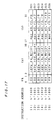
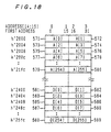
reference numeral 521 designates FM bits which are "00" since two instructions are executed in parallel. Thereference numerals reference numerals reference numeral 529 designates an area Ad for specifying the accumulator number of Adest. Fig. 17 illustrates the contents of the internal instruction memory corresponding to the loop part. For simplicity, the contents of the memory are expressed as mnemonics. The 32-bit instructions are referred to as I1 (511), I2 (512) and the like, and the short instructions are referred to as I1a (512(a)), I1b (512(b)) and the like. The six instructions I1 (511) to I6 (516) are repeatedly executed 42 times in the loop. - Fig. 18 illustrates mapping of the internal data memory with respect to the coefficients A[i] and data D[i]. Each area of the internal data memory holds 256 data. For the coefficients A[i], 16-bit data are held in 256-word (512-byte) areas at the
addresses 2000 to 21ff in hexadecimal. For the data D[i], 16-bit data are held in 256-word (512-byte) areas at theaddresses 2400 to 25ff in hexadecimal. - Fig. 19 (Figs. 19A to 19C) illustrates a flow of processing in the loop wherein the pipeline stages are depicted as the abscissa with time as the ordinate. All instructions are stored in the
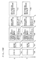
internal instruction memory 103, and all operand data are stored in theinternal data memory 105. One clock cycle is required to complete the processing at one stage. During the repeat processing continued, T1 follows T6. - Description is given on the basis of the processing of I1 (511). At the
IF stage 401, I1 (511) is fetched during T1 period (531). The contents of the IA register 181 are transferred to the instruction fetchunit 102. Thecomparator 187 compares the value in the IA register 181 with the value in theRPT_E 186. Since a mismatch occurs, the value in the IA register 181 is incremented by theincrementor 182 and written back. The instruction fetchunit 102 accesses theinternal instruction memory 103 to transmit the read 32-bit instruction data to the instruction queue 111. The instruction queue 111 transmits the instruction data transferred thereto within the same cycle to thefirst decoder 113 and thesecond decoder 114. - At the
D stage 402, I1 (511) is decoded during T2 period (537). Thefirst decoder 113 decodes the LD2W instruction of I1a (511(a)) to produce the control signal, and thesecond decoder 114 decodes the MAC instruction of I1b (511(b)) to produce the control signal. The control signals from the first andsecond decoders second operation units first operation unit 116. At theD stage 401, a conflict check is performed on the operands and arithmetic units, but no interference occurs. The value of the read operand of the MAC instruction has already been loaded. The MAC instruction of I1b (511(b)) is executed during T3 period (543). Writing a value to the register R0 has been completed during T1 period (535), and writing a value to the register R6 has been completed during T2 period (540). - At the
E stage 403, I1 (511) is executed during T3 period (543). Thefirst operation unit 116 produces the operand address of the LD2W instruction of I1a (511(a)) and updates the value of the address pointer. The value in the register R12 of theregister file 115 which is the operand address is transferred through theS3 bus 303 to theAA latch 151. The value in theAA latch 151 is intactly outputted to theoperand access unit 104 through the AO latch 154 andOA bus 321. The immediate value outputted form thefirst decoder 113 is transferred to theAB latch 152. TheALU 153 performs addition to write back the result of addition to the register R12 of theregister file 115 through theselector 155 andD1 bus 311. Thesecond operation unit 117 performs multiplication of the MAC instruction of I1b (511(b)). The value in the register R0 of theregister file 115 is applied to theX register 212 through theS4 bus 304, and the value in the register R6 of theregister file 115 is applied to theY register 213 through theS5 bus 305. Both of the values are handled as signed values and multiplied together. The result of multiplication is applied to theP register 214. - At the M and E2 stages 404 and 406, I1 (511) is subjected to memory access and addition during T4 period (549), respectively. The
operand access unit 104 loads the 4-byte data from theinternal data memory 105 at the address transmitted from thefirst operation unit 116 to transfer the fetched value to the LD register 164 through theOD bus 322. Thesecond operation unit 117 performs addition of the MAC instruction of I1b (511(b)). The value in the accumulator 208 (A0) is not shifted by theshifter 204 but is applied to theA latch 202. The value in theP register 214 is subjected to sign extension into 40 bits and applied to theB latch 203. TheALU 201 adds the values in the A and B latches 202 and 203 together to write back the result of addition to the accumulator 208 (A0). - At the
W stage 405, writing back to the register is performed during T5 period (555). Thefirst operation unit 116 outputs the data held in the LD register 164 to the W1 bus 314 andW2 bus 315 through thelatch 161 andalignment circuit 166. Since the operand is aligned in 4 bytes, the high-order 2 bytes are outputted to the W1 bus 314, and the low-order 2 bytes are outputted to theW2 bus 315. The data on the W1 bus 314 are written into the register R4 of theregister file 115, and the data on theW2 bus 315 are written into the register R5 of theregister file 115. - The pipeline processing of one 32-bit instruction for each clock cycle achieves one multiply-add operation for each clock cycle. In this manner, the loaded data value is written every two word into the registers R0 and R1 of the
register file 115 duringT1 period 535 at theW stage 405, and the loaded coefficient value is written every two word into the registers R6 and R7 of theregister file 115 duringT2 period 540 at theW stage 405. The value in the register R0 of theregister file 115 for holding the data and the value in the register R6 of theregister file 115 for holding the corresponding coefficient are referred to and multiplied together duringT3 period 543 at theE stage 403. The value in the register R1 of theregister file 115 for holding the data and the value in the register R7 of theregister file 115 for holding the corresponding coefficient are referred to and multiplied together duringT4 period 548 at theE stage 403. Such pipeline processing by means of software without operand interference improves the efficiency. - The repeat processing is not illustrated in detail in Fig. 19, but is described below briefly. At the
IF stage 401, the fetch address is compared with the last address of the repeat block. A match occurs duringT6 period 556 at theIF stage 401. The counter value ofRPT_C 188 which is not "1" indicates further repetition of the processing, and the processing sequence is changed. The value in thelatch 185 which is the start address of the block to be repeated is transferred to the IA register 181 through theJA bus 323. The instruction at the start address of the block to be repeated is fetched during T7 (not shown) period corresponding toT1 period 531 at theIF stage 401. The last instruction address match detection result of the repeat block is transferred through the pipeline. DuringT2 period 538 at theE stage 403 wherein I6 is executed, thedecrementor 190 decrements the value in therepeat counter RPT_C 188 by one independently of the instruction to be executed. If the value inRPT_C 188 before decrement is "1", the RP bit in the PSW is cleared to zero, and the repeat is disabled. - An n-stage second-order direct-form type II (n biquad) IIR (infinite impulse response) filter is described below. Fig. 20 illustrates the signal flow graph of the filter. In Fig. 20, 601 represents the multiplication of coefficients, 602 represents the addition of input data, and 603 represents a unit delay. Five multiply-add operations are executed within the loop. In this case, it is necessary to write the data of last two operations into the memory during the loop period. The data and coefficient each are 16 bits in length. Fig. 21 illustrates an example of a program of the IIR filter for the data processor of the first preferred embodiment. Initialization is performed at 606, the loop processing at 607, and the post-processing at 608. The loop processing without overhead is implemented by the repeat instruction.
- Processing in the loop is described in detail herein. Fig. 22 illustrates the contents of the internal instruction memory corresponding to the loop part. Six instructions I1 (611) to I7 (617) are executed repeatedly 42 times within the loop. An ST2W instruction at 611(a) directs that the memory stores the values in the two registers R0 and R1. The value in the register R12 serving as the base address is post-incremented. An MULX instruction at 611(b) directs that the values in the two registers R0 and R6 as signed values are multiplied together and the result of multiplication is written back into the accumulator. The result of multiplication is written back into the
accumulator 208 within the same cycle through theselector 207. An ADD instruction at 612(a) directs that theALU 201 adds 4 to the contents of the register R12. An MV instruction at 613(b) directs that the value of r4 is copied to r1. An MV2W instruction at 616(b) transfers two words, that is, transfers the values in the registers R4 and R5 to the registers R2 and R3, respectively. Since the data are transferred through thebarrel shifter 215 in this case, a hardware resource does not interfere with the immediately preceding multiply-add operation instruction. An RACHI instruction at 617(b) directs that the value in the accumulator A0 is 1 bit left-shifted, rounded to upper 16 bits, limited on the basis of the value of the guard bits to a maximum value h'7fff expressible in 16 bits if an overflow occurs and to a minimum value h'8000 expressible in 16 bits if an underflow occurs, and written back to the register R0. This operation is executed by using theALU 201 andsaturation circuit 209. - The register R0 holds input data to the next stage. The register R1 is used as update data Di1 (i is an integer not more than n). The registers R2 to R5 are used as a buffer for holding the data. The registers R6, and R8 to R11 are used as a buffer for coefficients. The register R12 is used as a data pointer. The register R14 is used as a pointer for coefficients. The register R7 holds invalid data to maintain 32-bit alignment of the coefficient data.
- Fig. 23 illustrates mapping of the internal data memory with respect to the coefficients and data. The respective data are 16 bits in length. Five coefficients are provided per stage and two data are provided per stage in the arrangement of Fig. 20. A coefficient Ai (621) is to be multiplied by an input value. The
reference numerals - Fig. 24 (Figs. 24A to 24C) illustrates a flow of processing within the loop wherein the pipeline stages are depicted as the abscissa with time as the ordinate. All instructions are stored in the
internal instruction memory 103, and all operand data are stored in theinternal data memory 105. One clock cycle is required to complete the processing at one stage. During the repeat processing continued, T1 follows T7. As is the case with the above described FIR filter, the fetched data are referred to at least 2 cycles later. The instruction at 611 directs that multiplication is executed simultaneously as two words are stored for data updating. The MV2W instruction directs that the contents of data are transferred every two word at a time (at 643) so that the same register number is used each time the loop is repeated. The value in the register R4 loaded at 659 during T4 period and the value in the register R10 loaded at 655 during T3 period are multiplied together at 666 during T6 period, and the value in the register R5 loaded at 659 during T4 period and the value in the register R11 loaded at 655 during T3 period are multiplied together at 670 during T7 period. Such processing allows 7 cycles to be required to implement the processing of the second-order direct-form type-II IIR filter at one stage. - An example of IFFT (inverse fast Fourier transform) is described below. Unit processing is as follows:
- Fig. 25 illustrates an example of a program in a loop part when two unit processings of the IFFT form one loop. The registers R0, R1, and R2, R3 hold a and A. The registers R4 and R5 hold b. The registers R6 and R7 hold tmp. The registers R8 and R9 hold a and B. The registers R10 and R11 hold c. The even-numbered registers hold the real part, and the odd-numbered registers hold the imaginary part. The register R12 holds the address of a. The register R14 holds the address of b.
- The symbol "msu" indicates the multiply-subtract instruction which directs that the result of multiplication is subtracted from the accumulator. This is because the square of i (complex number) equals -1.
- In this case, 15 cycles are required to implement two unit processings with respect to two pairs of complex numbers. The thirty sub-instructions include four 2-word load instructions, four 2-word store instructions, four additions, four subtractions, four multiplications, two multiply-add operations, two multiply-subtract operations, four rounding instructions, and two 2-word transfer instructions, providing very high efficiency of operations.
- Fig. 26 illustrates an example of a program in a loop part of a subtract-absolute-add operation. An absadd instruction directs that the specified register value is applied from the
register file 115 to the low-order positions of theshifter 205 through theS5 bus 305. Theshifter 205 performs sign extension on the value into 40 bits but does not shift the value to apply the value to theB latch 203. The value is subjected to the operation with the value in theaccumulator 208 specified by theALU 201, and the result of the operation is written back to theaccumulator 208. TheALU 201 performs addition when the value in theB latch 203 is positive, and performs subtraction when the value is negative. The subtraction is implemented by inverting the data and providing a carry to the least significant bit. In this manner, one clock cycle is required to implement the absolute-add operation. - Fig. 27 (Figs. 27A to 27C) illustrates a flow of processing in the loop. The 2-word load instruction is executed in parallel with the absolute-add instruction of the result of subtraction. During T3 cycle, data are loaded to the registers R6 and R7 in response to the LD2W instruction of 15a (813). Then, during T4 cycle, data are loaded to the registers R2 and R3 in response to the LD2W instruction of 16a (817). During T6 cycle, the value in the register R7 is subtracted form the value in the register R3 in response to the instruction indicated by I4a, and the result of subtraction is written back to the register R3. Further, the value in the register R6 is subtracted from the value in the register R2 in parallel in response to the instruction indicated by I4b, and the result of subtraction is written back to the register R2 (824). In this manner, four subtract-absolute-add operations are implemented in 6 cycles.
- Fig. 28 is a block diagram of a
second operation unit 120 for the data processor according to a second preferred embodiment of the present invention corresponding to thesecond operation unit 117 of the first preferred embodiment. Other units of the data processor of the second preferred embodiment are similar in construction to those of the first preferred embodiment. Thesecond operation unit 120 differs from thesecond operation unit 117 of the first preferred embodiment in that it includes anALU 221 operable independently of anadder 231 for performing the multiply-add operation. This allows the execution of the addition and subtraction of the multiply-add/multiply-subtract instructions and other arithmetic and logic operations without interference of hardware. - The
ALU 221 performs a 16-bit arithmetic and logic operation. AnA2 latch 222 connected to theS4 bus 304 and aB2 latch 223 connected to theS5 bus 305 are input latches for theALU 221. AnALUO latch 225 is an output latch for theALU 221. Aselector 224 selects the output from theALU 221, the value in theA2 latch 222, or the value in theB2 latch 223 to write back the selected value to theregister file 115 through theD2 bus 312. The output from theALUO latch 225 may be set to the low-order positions and subjected to sign extension by ashifter 235.A B latch 233 selectively receives the output from theshifter 235 or the value in theP latch 214 serving as the output latch of themultiplier 211. AnA latch 232 receives data from theaccumulator 208 through theshifter 204. Other elements of thesecond operation unit 120 are substantially identical with those of thesecond operation unit 117 of the first preferred embodiment. - An example of processing is described below. Fig. 29 illustrates an exemplary program of a subtract-square-add operation. Initialization is performed at 701, the loop processing at 702, and the post-processing at 703. Fig. 30 illustrates the contents of the internal instruction memory corresponding to the loop part. The substract-square-accumulate operation of D1[i] and D2[i] is performed. The register R12 holds the address of D1[i], and the register R14 holds the address of D2[i]. The registers R0 to R3 hold the data D1[i], and the registers R4 to R7 hold the data D2[i]. All instructions are executed in parallel. Six cycles are required to execute the processing four times. Fig. 31 illustrates mapping of the internal data memory with respect to the data. The respective data are 16 bits in length. The data D1[i] and D2[i] are stored in different areas.
- Fig. 32 (Figs. 32A to 32C) illustrates a flow of processing in the loop. For example, the
adder 231 and theALU 221 execute the addition (746) of the multiply-add operation and the subtraction (745) for determining the difference in parallel during T6 period. - The data processor of the second preferred embodiment may more efficiently process the subtract-absolute-add operation described in the first preferred embodiment. Fig. 33 illustrates the contents of the internal instruction memory corresponding to the loop part. The register R12 holds the address of a first data array, and the registers R0 to R5 hold the data thereof. The register R14 holds the address of a second data array, and the registers R6 to R11 hold the data thereof. An daadd instruction is an instruction for determining the subtract-absolute-add operation, and the result of the operation is held in the accumulator. This instruction, like the multiply-add operation instruction, directs that two-stage pipeline processing is executed.
- Fig. 34 (Figs. 34A to 34C) illustrates a flow of processing in the loop. The processing conditions in Fig. 34 are substantially similar to those in the case of the FIR filter described in the first preferred embodiment. The subtract-absolute-add operation is executed in Fig. 34 in place of the multiply-add operation. That is, multiplication is replaced with subtraction, and the addition is replaced with the absolute-add operation. In this manner, the throughput of the processing is such that one subtract-absolute-add operation is executed per cycle.
- Fig. 35 is a functional block diagram of the data processor according to a third preferred embodiment of the present invention. An MPU 850 is an MPU core. An instruction fetch unit 863 and an
operand access unit 864 are substantially similar to the instruction fetchunit 102 andoperand access unit 104 of the data processor of the first preferred embodiment. The instruction data which are 64 bits in length are applied to the instruction fetch unit 863. The bus interface unit and the like are not shown in Fig. 35. - The MPU core 850 comprises an
instruction queue 851, acontrol unit 852, aregister file 860, afirst operation unit 858, asecond operation unit 859, athird operation unit 861, and afourth operation unit 862. Theinstruction queue 851 is an FIFO-controlled instruction buffer for holding a maximum of two 64-bit instructions. Thefirst operation unit 858 includes an incrementor, a decrementor, and an adder and performs management of the PC value, calculation of the branch target address, and repeat control. Thesecond operation unit 859 includes an ALU and an alignment circuit and performs operand address generation, updating of the pointer, arithmetic and logic operations, transfer, comparison, holding and alignment of loaded data, and holding and alignment of data to be stored. Thethird operation unit 861 includes an ALU and a shifter, and performs operation processing such as arithmetic and logic operations, transfer, comparison and shift. Thefourth operation unit 862 includes a multiply-add operation unit, a shifter, and an accumulator, and mainly performs the multiply-add and multiply-subtract operations and accumulator shift. In this manner, the MPU core 850 has the four independent arithmetic units connected to the register file. - The
control unit 852 includes aninstruction decode unit 853. Theinstruction decode unit 853 has four decoders. Fig. 36 illustrates an instruction format processed by the data processor of the third preferred embodiment.FM bits 871 having a 4-bit format are divided into two 2 bits for specifying the formats of the combination of first andsecond containers fourth containers fourth containers 872 to 875 is expressed in 15 bits. - The
first decoder 854 mainly decodes the operation code of thefirst container 872 to produce control signals for theregister file 860 andfirst operation unit 858. The branch instruction is mainly specified in the field of thefirst container 872. Thesecond decoder 855 mainly decodes the operation code of thesecond container 873 to produce control signals for theregister file 860 andsecond operation unit 859. The load/store instruction, arithmetic and logic operation instruction, transfer instruction, and comparison instruction are mainly specified in the field of thesecond container 873. Thethird decoder 856 mainly decodes the operation code of thethird container 874 to produce control signals for theregister file 860 andthird operation unit 861. The arithmetic and logic operation instruction, transfer instruction, comparison instruction, and shift instruction are mainly specified in the field of thethird container 874. The fourth decoder 857 mainly decodes the operation code of thefourth container 875 to produce control signals for theregister file 860 andfourth operation unit 862. The multiply-add operation instruction is mainly specified in the field of thefourth container 875. - Such an arrangement allows greatly sophisticated parallel processing. The present invention is applicable also in such a case. For example, to execute the subtract-square-add operation, the second, third, and
fourth operation units - For improvement in the throughput of the multiply-add operation, a plurality of operation units should have multiply-add operation units to increase the number of operands to be transferred. The present invention is also applicable in this case.
- Fig. 37 is a block diagram of the
second operation unit 120 of the data processor according to a fourth preferred embodiment of the present invention corresponding to thesecond operation unit 117 of the data processor of the first preferred embodiment. Other units of the data processor of the fourth preferred embodiment are substantially identical in construction with those of the first preferred embodiment. - In the fourth preferred embodiment, the result of the multiply-add operation is stored in the register for each operation, and no guard bits are provided. Additional guard bits may be provided if required in terms of operation accuracy.
- Fig. 38 illustrates an instruction format for the data processor of the fourth preferred embodiment wherein the instruction is 64 bits in length. The instruction comprises 2
FM bits 941, a 31-bit left-hand container 942, and a 31-bit right-hand container 943. Fig. 39 illustrates a basic format of each container which is basically a 3-operand format including three fields: two source registernumber specification fields number specification field 945. There are provided 64 registers, and the register number is specified in a 6-bit field. - The basic pipeline processing of the fourth preferred embodiment is similar to that of the first preferred embodiment, and the description thereof will be dispensed with. An S4 bus 913, an S5 bus 914, a
D2 bus 915, and aD3 bus 916 operate at theE stage 403. These buses mainly transfer operand values of an ordinary integer operation instruction and the like. An S6 bus 911, an S7 bus 912, aD4 bus 917, and aD5 bus 918 operate at theE2 stage 406. These buses mainly transfer accumulated value. Anadder 934 and its input and output units operate at theE stage 403 andE2 stage 406, but other arithmetic units and latches operate at theE stage 403. - A "mac" instruction for multiply-add operation is a 3-operand instruction. The processing specifications of "mac Rdest, Rsrc1, Rsrc2" are such that the register value specified by Rsrc1 and the register value specified by Rsrc2 are multiplied together and the result of multiplication is added to the value in the pair of registers specified by Rdest. The hardware processing is described in detail. First, at the
E stage 403, the register values specified by Rsrc1 and Rsrc2 are transferred from aregister file 903 through the S4 bus 913 and S5 bus 914 to anX latch 938 and aY latch 939, respectively. Amultiplier 940 performs multiplication, and theP register 941 holds the result of multiplication. Then, at theE2 stage 406, the values in the pair of registers specified by Rdest is applied to anA latch 931 from theregister file 903 through the S6 bus 911, the S7 bus 912, and theshifter 930. The value in theP register 941 is applied to aB latch 933. Theadder 934 adds the values in theA latch 931 andB latch 933 together. The result of addition is outputted through asaturation circuit 937 to theD4 bus 917 andD5 bus 918, and written back to the pair of registers specified by Rdest in theregister file 903. - Fig. 40 illustrates an example of the program in a loop part of the FIR filter. The 2-word load instruction and the multiply-add operation instruction are decoded in parallel and executed in parallel. This achieves one multiply-add operation per cycle in the same manner as in the data processor of the first preferred embodiment except that the result of the multiply-add operation is written back to the register file for each operation.
- In this manner, the technique of the present invention is also effective when the cumulative result of the multiply-add operations is held in the register. The operands are not bypassed herein, but a bypass path may be provided as required.
- In the data processor of the above described preferred embodiments, one word is assumed to be 16 bits in length. However, one word may be any number of bits in length. For example, audio processing requires about 24 bits in length, and one word may be 24 bits in length. One word may be 32 bits long in terms of alignment with a processor. In this case, the multiplier may not necessarily be of 1-word by 1-word form, but a multiplier of a size essential in terms of the accuracy of an application to be processed should be selected and implemented.
- In the data processor of the above described preferred embodiments, the multiply-add operation is subjected to two-stage pipeline processing. However, the last addition stage of the multiplier and the adder for addition may be merged to execute the multiply-add operation in one cycle. Additionally, for high-speed operation, the multiplication may be performed by 2-stage pipeline to permit the multiply-add operation to be performed by 3-stage pipeline. Other pipelines may be freely selectable. For instance, the
E stage 403 andM stage 404 may be merged into one pipeline stage for processing. Further, to improve the operating frequency, write back operation to the register may be performed in the different pipeline stage from E stage. In addition, data may be bypassed from the write path to the register, which is effective for high-speed processing. - In the above described preferred embodiments of the present invention, the microprocessor of VLIW architecture is illustrated as an example. However, the technique of the present invention is also applicable to a superscalar RISC processor and the like programmed if the details of hardware are noted and the conditions for parallel processing are seized. The difference is that the parallel execution is encoded in the program or the hardware determines whether or not the parallel execution is permitted. The FM bits may be absent in the VLIW architecture. The instructions may be always executed in parallel. In this case, the operation which is not executed in parallel should be set to NOP.
- While the invention has been described in detail, the foregoing description is in all aspects illustrative and not restrictive. It is understood that numerous other modifications and variations can be devised without departing from the scope of the invention as defined by the appended claims.
Claims (9)
- A data processor comprising:characterized in thatan instruction decode unit (119) receiving instructions including first and second operation codes, the instruction decode unit (119) including first and second decoders (113, 114) for decoding the first and second operation codes, respectively;a first operation unit (116) for executing a first operation in accordance with a decoded result of the first decoder (113);a second operation unit (117) for executing a second operation in accordance with a decoded result of the second decoder (114);a register file (115) including a plurality of registers; andan operand access unit (104) for accessing a memory (105),when the first and second decoders (113, 114), respectively, decode the first operation code specifying a data load operation and the second operation code specifying a multiply-add operation,the first operation unit (116) generates an address to be output to the memory (105),the second operation unit (117) executes the multiply-add operation including a multiplying operation of first data by second data and adding operation of third data to a result of the multiplying operation, the first and second data each having n bits and are stored in the register file (115), andthe operand access unit (104) reads operand data stored in a location specified by the address from the memory (105) during an execution of the multiply-add operation by the second operation unit (117), the operand data including at least data of 2n bits, the operand data being transferred to the register file (115).
- The data processor of claim 1,
wherein upper n bits and lower n bits of the data of 2n bits in the operand data are transferred to first and second registers among the plurality of registers, respectively, and the first and second data are stored in third and fourth registers among the plurality of registers, respectively. - The data processor of claim 1 or 2,
wherein the second operation unit (117) includes a multiplier (211) for performing the multiplying operation and an adder (201) for performing the adding operation. - The data processor of claim 3,
wherein the second operation unit (117) further includes an accumulator (208) for storing the third data, and the stored third data are updated into a result of the addition. - The data processor of claim 3,
wherein the third data are stored in a fifth register among the plurality of registers and updated into a result of the addition. - The data processor of any of claims 1 to 5,
wherein the first operation unit (116) outputs the address in parallel with the multiplying operation by the second operation unit (117). - The data processor of any of claims 1 to 6,
wherein the operand access unit (104) receives the operand data in parallel with the adding operation of the second operation unit (117). - The data processor of any of claims 1 to 7,
wherein the first operation unit (116) generates the address by receiving the address from the register file (115), the address stored in a sixth register among the plurality of registers. - The data processor of any of claims 1 to 8,
wherein the first operation unit (116) generates the address in one cycle,
the operand access unit (104) reads the operand data from the memory and transfers the operand data to the register file (115) in one cycle, and
the second operation unit (117) executes the multiplying and adding operations in one cycle.
Priority Applications (1)
| Application Number | Priority Date | Filing Date | Title |
|---|---|---|---|
| EP02013414A EP1265131A3 (en) | 1996-02-07 | 1996-12-05 | Digital signal processor and method of processing digital signal data |
Applications Claiming Priority (3)
| Application Number | Priority Date | Filing Date | Title |
|---|---|---|---|
| JP21453/96 | 1996-02-07 | ||
| JP2145396 | 1996-02-07 | ||
| JP02145396A JP3658072B2 (en) | 1996-02-07 | 1996-02-07 | Data processing apparatus and data processing method |
Related Child Applications (1)
| Application Number | Title | Priority Date | Filing Date |
|---|---|---|---|
| EP02013414A Division EP1265131A3 (en) | 1996-02-07 | 1996-12-05 | Digital signal processor and method of processing digital signal data |
Publications (3)
| Publication Number | Publication Date |
|---|---|
| EP0789297A2 EP0789297A2 (en) | 1997-08-13 |
| EP0789297A3 EP0789297A3 (en) | 1998-12-02 |
| EP0789297B1 true EP0789297B1 (en) | 2003-05-02 |
Family
ID=12055391
Family Applications (2)
| Application Number | Title | Priority Date | Filing Date |
|---|---|---|---|
| EP02013414A Withdrawn EP1265131A3 (en) | 1996-02-07 | 1996-12-05 | Digital signal processor and method of processing digital signal data |
| EP96119559A Expired - Lifetime EP0789297B1 (en) | 1996-02-07 | 1996-12-05 | Data processor loading data and performing multiply-add operation in parallel |
Family Applications Before (1)
| Application Number | Title | Priority Date | Filing Date |
|---|---|---|---|
| EP02013414A Withdrawn EP1265131A3 (en) | 1996-02-07 | 1996-12-05 | Digital signal processor and method of processing digital signal data |
Country Status (4)
| Country | Link |
|---|---|
| US (2) | US5901301A (en) |
| EP (2) | EP1265131A3 (en) |
| JP (1) | JP3658072B2 (en) |
| DE (1) | DE69627807T2 (en) |
Families Citing this family (63)
| Publication number | Priority date | Publication date | Assignee | Title |
|---|---|---|---|---|
| US6219779B1 (en) * | 1997-06-16 | 2001-04-17 | Matsushita Electric Industrial Co., Ltd. | Constant reconstructing processor which supports reductions in code size |
| JP3412462B2 (en) * | 1997-07-30 | 2003-06-03 | 松下電器産業株式会社 | Processor |
| US6101592A (en) * | 1998-12-18 | 2000-08-08 | Billions Of Operations Per Second, Inc. | Methods and apparatus for scalable instruction set architecture with dynamic compact instructions |
| US6324639B1 (en) | 1998-03-30 | 2001-11-27 | Matsushita Electric Industrial Co., Ltd. | Instruction converting apparatus using parallel execution code |
| US6418529B1 (en) * | 1998-03-31 | 2002-07-09 | Intel Corporation | Apparatus and method for performing intra-add operation |
| US6212618B1 (en) * | 1998-03-31 | 2001-04-03 | Intel Corporation | Apparatus and method for performing multi-dimensional computations based on intra-add operation |
| US7395302B2 (en) | 1998-03-31 | 2008-07-01 | Intel Corporation | Method and apparatus for performing horizontal addition and subtraction |
| US7392275B2 (en) * | 1998-03-31 | 2008-06-24 | Intel Corporation | Method and apparatus for performing efficient transformations with horizontal addition and subtraction |
| US6801995B1 (en) * | 1998-08-04 | 2004-10-05 | Agere Systems, Inc. | Method for optimally encoding a set of instruction codes for a digital processor having a plurality of instruction selectable resource types and an associated optimized set of instruction codes |
| US7114056B2 (en) | 1998-12-03 | 2006-09-26 | Sun Microsystems, Inc. | Local and global register partitioning in a VLIW processor |
| US7117342B2 (en) * | 1998-12-03 | 2006-10-03 | Sun Microsystems, Inc. | Implicitly derived register specifiers in a processor |
| US6615338B1 (en) * | 1998-12-03 | 2003-09-02 | Sun Microsystems, Inc. | Clustered architecture in a VLIW processor |
| JP3842474B2 (en) | 1999-02-02 | 2006-11-08 | 株式会社ルネサステクノロジ | Data processing device |
| US6504495B1 (en) * | 1999-02-17 | 2003-01-07 | Arm Limited | Clipping data values in a data processing system |
| DE50014621D1 (en) * | 1999-05-06 | 2007-10-18 | Siemens Ag | Communication device with means for real-time processing of payload data to be transmitted |
| US6820189B1 (en) * | 1999-05-12 | 2004-11-16 | Analog Devices, Inc. | Computation core executing multiple operation DSP instructions and micro-controller instructions of shorter length without performing switch operation |
| JP2002544587A (en) * | 1999-05-12 | 2002-12-24 | アナログ デバイセス インコーポレーテッド | Digital signal processor calculation core |
| US7107302B1 (en) | 1999-05-12 | 2006-09-12 | Analog Devices, Inc. | Finite impulse response filter algorithm for implementation on digital signal processor having dual execution units |
| US6859872B1 (en) | 1999-05-12 | 2005-02-22 | Analog Devices, Inc. | Digital signal processor computation core with pipeline having memory access stages and multiply accumulate stages positioned for efficient operation |
| US7111155B1 (en) | 1999-05-12 | 2006-09-19 | Analog Devices, Inc. | Digital signal processor computation core with input operand selection from operand bus for dual operations |
| JP2001022689A (en) * | 1999-07-06 | 2001-01-26 | Mitsubishi Electric Corp | Output fifo data transfer control device |
| US6446195B1 (en) * | 2000-01-31 | 2002-09-03 | Intel Corporation | Dyadic operations instruction processor with configurable functional blocks |
| US6330660B1 (en) * | 1999-10-25 | 2001-12-11 | Vxtel, Inc. | Method and apparatus for saturated multiplication and accumulation in an application specific signal processor |
| US6832306B1 (en) | 1999-10-25 | 2004-12-14 | Intel Corporation | Method and apparatus for a unified RISC/DSP pipeline controller for both reduced instruction set computer (RISC) control instructions and digital signal processing (DSP) instructions |
| US6408376B1 (en) | 1999-10-25 | 2002-06-18 | Intel Corporation | Method and apparatus for instruction set architecture to perform primary and shadow digital signal processing sub-instructions simultaneously |
| US6557096B1 (en) | 1999-10-25 | 2003-04-29 | Intel Corporation | Processors with data typer and aligner selectively coupling data bits of data buses to adder and multiplier functional blocks to execute instructions with flexible data types |
| WO2001052183A1 (en) * | 2000-01-07 | 2001-07-19 | Intensys Corporation | Method and apparatus to transform specification of functions for processing grid-structured data |
| US6732203B2 (en) * | 2000-01-31 | 2004-05-04 | Intel Corporation | Selectively multiplexing memory coupling global bus data bits to narrower functional unit coupling local bus |
| US6959222B1 (en) * | 2000-04-13 | 2005-10-25 | New Japan Radio Co., Ltd. | Accelerator engine for processing functions used in audio algorithms |
| JP3845814B2 (en) * | 2000-08-10 | 2006-11-15 | 株式会社テルミナス・テクノロジー | Associative memory, search method thereof, router and network system |
| JP2002073330A (en) | 2000-08-28 | 2002-03-12 | Mitsubishi Electric Corp | Data processing device |
| US7003093B2 (en) * | 2000-09-08 | 2006-02-21 | Intel Corporation | Tone detection for integrated telecommunications processing |
| US20020116186A1 (en) * | 2000-09-09 | 2002-08-22 | Adam Strauss | Voice activity detector for integrated telecommunications processing |
| JP2002229779A (en) | 2001-02-02 | 2002-08-16 | Mitsubishi Electric Corp | Information processor |
| JP4502532B2 (en) * | 2001-02-23 | 2010-07-14 | 株式会社ルネサステクノロジ | Data processing device |
| US20030219113A1 (en) * | 2002-05-21 | 2003-11-27 | Bershad Neil J. | Echo canceller with double-talk and channel impulse response adaptation |
| US7380151B1 (en) | 2002-12-11 | 2008-05-27 | National Semiconductor Corporation | Apparatus and method for asynchronously clocking the processing of a wireless communication signal by multiple processors |
| US7016695B1 (en) | 2002-12-11 | 2006-03-21 | National Semiconductor Corporation | Apparatus and method for processing a deterministic data flow associated with a wireless communication signal |
| US7366352B2 (en) * | 2003-03-20 | 2008-04-29 | International Business Machines Corporation | Method and apparatus for performing fast closest match in pattern recognition |
| US7194601B2 (en) * | 2003-04-03 | 2007-03-20 | Via-Cyrix, Inc | Low-power decode circuitry and method for a processor having multiple decoders |
| US7680990B2 (en) * | 2003-05-30 | 2010-03-16 | Hewlett-Packard Development Company, L.P. | Superword memory-access instructions for data processor |
| US7017127B1 (en) | 2003-06-02 | 2006-03-21 | National Semiconductor Corporation | Method and system for enabling energy efficient wireless connectivity |
| US7793072B2 (en) * | 2003-10-31 | 2010-09-07 | International Business Machines Corporation | Vector execution unit to process a vector instruction by executing a first operation on a first set of operands and a second operation on a second set of operands |
| US8484441B2 (en) | 2004-03-31 | 2013-07-09 | Icera Inc. | Apparatus and method for separate asymmetric control processing and data path processing in a configurable dual path processor that supports instructions having different bit widths |
| US7949856B2 (en) * | 2004-03-31 | 2011-05-24 | Icera Inc. | Method and apparatus for separate control processing and data path processing in a dual path processor with a shared load/store unit |
| US9047094B2 (en) * | 2004-03-31 | 2015-06-02 | Icera Inc. | Apparatus and method for separate asymmetric control processing and data path processing in a dual path processor |
| US7437536B2 (en) * | 2004-05-03 | 2008-10-14 | Sony Computer Entertainment Inc. | Systems and methods for task migration |
| JP2006004042A (en) * | 2004-06-16 | 2006-01-05 | Renesas Technology Corp | Data processor |
| US7205923B1 (en) | 2004-12-07 | 2007-04-17 | National Semiconductor Corporation | Pipelined analog to digital converter that is configurable based on mode and strength of received signal |
| US6980148B1 (en) | 2004-12-07 | 2005-12-27 | National Semiconductor Corporation | Pipelined analog to digital converter that is configurable based on wireless communication protocol |
| US7193553B1 (en) | 2004-12-07 | 2007-03-20 | National Semiconductor Corporation | Analog to digital converter with power-saving adjustable resolution |
| GB2421092B (en) * | 2004-12-07 | 2008-12-03 | Hewlett Packard Development Co | Bufferless writing of data to memory |
| US7370136B2 (en) * | 2005-01-26 | 2008-05-06 | Stmicroelectronics, Inc. | Efficient and flexible sequencing of data processing units extending VLIW architecture |
| US7581082B2 (en) * | 2005-05-13 | 2009-08-25 | Texas Instruments Incorporated | Software source transfer selects instruction word sizes |
| US7912887B2 (en) * | 2006-05-10 | 2011-03-22 | Qualcomm Incorporated | Mode-based multiply-add recoding for denormal operands |
| GB2464292A (en) * | 2008-10-08 | 2010-04-14 | Advanced Risc Mach Ltd | SIMD processor circuit for performing iterative SIMD multiply-accumulate operations |
| US8161090B2 (en) * | 2008-12-05 | 2012-04-17 | Crossfield Technology LLC | Floating-point fused add-subtract unit |
| KR101401244B1 (en) * | 2009-09-04 | 2014-05-28 | 실리콘 하이브 비.브이. | Method and apparatus and record carrier |
| JP6050721B2 (en) * | 2012-05-25 | 2016-12-21 | 株式会社半導体エネルギー研究所 | Semiconductor device |
| EP3005078A2 (en) * | 2013-05-24 | 2016-04-13 | Coherent Logix Incorporated | Memory-network processor with programmable optimizations |
| JP6378515B2 (en) * | 2014-03-26 | 2018-08-22 | 株式会社メガチップス | VLIW processor |
| JP2017228213A (en) * | 2016-06-24 | 2017-12-28 | 富士通株式会社 | Arithmetic processing unit and control method of arithmetic processing unit |
| US11417373B2 (en) | 2020-12-09 | 2022-08-16 | Micron Technology, Inc. | Neuromorphic computing devices and methods |
Family Cites Families (24)
| Publication number | Priority date | Publication date | Assignee | Title |
|---|---|---|---|---|
| JPS5344130A (en) * | 1976-10-05 | 1978-04-20 | Toshiba Corp | Floating access memory device |
| JPS57113144A (en) * | 1980-12-30 | 1982-07-14 | Seiko Epson Corp | Stored program computer |
| JPS60134938A (en) * | 1983-12-23 | 1985-07-18 | Nec Corp | Register file reading system |
| JPS60138640A (en) * | 1983-12-27 | 1985-07-23 | Nec Corp | Writing system of register file |
| US4819152A (en) * | 1985-04-05 | 1989-04-04 | Raytheon Company | Method and apparatus for addressing a memory by array transformations |
| JPH0719246B2 (en) * | 1988-01-11 | 1995-03-06 | 三洋電機株式会社 | Digital signal processor |
| US5201039A (en) * | 1987-09-30 | 1993-04-06 | Mitsubishi Denki Kabushiki Kaisha | Multiple address-space data processor with addressable register and context switching |
| US4862407A (en) * | 1987-10-05 | 1989-08-29 | Motorola, Inc. | Digital signal processing apparatus |
| US5134711A (en) * | 1988-05-13 | 1992-07-28 | At&T Bell Laboratories | Computer with intelligent memory system |
| NL8902040A (en) * | 1988-08-19 | 1990-03-16 | Tektronix Inc | HIGH SPEED DIRECT MEMORY ACCESS CONTROL FOR TEST AND MEASUREMENT INSTRUMENTS. |
| JPH02103632A (en) * | 1988-10-12 | 1990-04-16 | Nec Corp | Arithmetic processor |
| JP2816248B2 (en) * | 1989-11-08 | 1998-10-27 | 株式会社日立製作所 | Data processor |
| JPH03186928A (en) * | 1989-12-16 | 1991-08-14 | Mitsubishi Electric Corp | Data processor |
| US5299321A (en) * | 1990-12-18 | 1994-03-29 | Oki Electric Industry Co., Ltd. | Parallel processing device to operate with parallel execute instructions |
| KR950015181B1 (en) * | 1991-07-01 | 1995-12-23 | 후지쓰 가부시끼가이샤 | Apparatus for sum-of-product operation |
| JPH05233281A (en) * | 1992-02-21 | 1993-09-10 | Toshiba Corp | Electronic computer |
| US5485629A (en) * | 1993-01-22 | 1996-01-16 | Intel Corporation | Method and apparatus for executing control flow instructions in a control flow pipeline in parallel with arithmetic instructions being executed in arithmetic pipelines |
| US5825921A (en) * | 1993-03-19 | 1998-10-20 | Intel Corporation | Memory transfer apparatus and method useful within a pattern recognition system |
| JPH07114469A (en) * | 1993-10-18 | 1995-05-02 | Mitsubishi Electric Corp | Data processing unit |
| EP0651321B1 (en) * | 1993-10-29 | 2001-11-14 | Advanced Micro Devices, Inc. | Superscalar microprocessors |
| JPH07176380A (en) | 1993-12-21 | 1995-07-14 | Casio Comput Co Ltd | Electroluminescent element |
| US5630083A (en) * | 1994-03-01 | 1997-05-13 | Intel Corporation | Decoder for decoding multiple instructions in parallel |
| US5812810A (en) * | 1994-07-01 | 1998-09-22 | Digital Equipment Corporation | Instruction coding to support parallel execution of programs |
| JP2931890B2 (en) | 1995-07-12 | 1999-08-09 | 三菱電機株式会社 | Data processing device |
-
1996
- 1996-02-07 JP JP02145396A patent/JP3658072B2/en not_active Expired - Lifetime
- 1996-08-20 US US08/699,944 patent/US5901301A/en not_active Ceased
- 1996-12-05 EP EP02013414A patent/EP1265131A3/en not_active Withdrawn
- 1996-12-05 DE DE69627807T patent/DE69627807T2/en not_active Expired - Lifetime
- 1996-12-05 EP EP96119559A patent/EP0789297B1/en not_active Expired - Lifetime
-
2001
- 2001-05-04 US US09/848,253 patent/USRE38679E1/en not_active Expired - Lifetime
Also Published As
| Publication number | Publication date |
|---|---|
| JPH09212361A (en) | 1997-08-15 |
| JP3658072B2 (en) | 2005-06-08 |
| EP0789297A3 (en) | 1998-12-02 |
| EP1265131A2 (en) | 2002-12-11 |
| DE69627807T2 (en) | 2004-03-11 |
| DE69627807D1 (en) | 2003-06-05 |
| EP0789297A2 (en) | 1997-08-13 |
| EP1265131A3 (en) | 2007-05-30 |
| USRE38679E1 (en) | 2004-12-28 |
| US5901301A (en) | 1999-05-04 |
Similar Documents
| Publication | Publication Date | Title |
|---|---|---|
| EP0789297B1 (en) | Data processor loading data and performing multiply-add operation in parallel | |
| US6560697B2 (en) | Data processor having repeat instruction processing using executed instruction number counter | |
| US5923871A (en) | Multifunctional execution unit having independently operable adder and multiplier | |
| US7937559B1 (en) | System and method for generating a configurable processor supporting a user-defined plurality of instruction sizes | |
| US5826089A (en) | Instruction translation unit configured to translate from a first instruction set to a second instruction set | |
| US5638524A (en) | Digital signal processor and method for executing DSP and RISC class instructions defining identical data processing or data transfer operations | |
| US6016543A (en) | Microprocessor for controlling the conditional execution of instructions | |
| US20070174596A1 (en) | Data processor | |
| US20070239967A1 (en) | High-performance RISC-DSP | |
| JP3856737B2 (en) | Data processing device | |
| JP3745039B2 (en) | Microprocessor with delayed instructions | |
| JPH10116268A (en) | Single-instruction plural data processing using plural banks or vector register | |
| US6484253B1 (en) | Data processor | |
| JP2001501330A (en) | Digital signal processing integrated circuit architecture | |
| JPH0766324B2 (en) | Data processing device | |
| JPH1049368A (en) | Microporcessor having condition execution instruction | |
| US5924114A (en) | Circular buffer with two different step sizes | |
| JP3578883B2 (en) | Data processing device | |
| US7010677B2 (en) | Data processor speeding up repeat processing by inhibiting remaining instructions after a break in a repeat block | |
| US6078940A (en) | Microprocessor with an instruction for multiply and left shift with saturate | |
| JP4502532B2 (en) | Data processing device | |
| JP2001501755A (en) | Data processing condition code flag | |
| JP2522048B2 (en) | Microprocessor and data processing device using the same | |
| Dandamudi | Arm architecture | |
| JPH10320199A (en) | Microprocessor with conditioned execution instruction |
Legal Events
| Date | Code | Title | Description |
|---|---|---|---|
| PUAI | Public reference made under article 153(3) epc to a published international application that has entered the european phase |
Free format text: ORIGINAL CODE: 0009012 |
|
| AK | Designated contracting states |
Kind code of ref document: A2 Designated state(s): DE FR GB |
|
| PUAL | Search report despatched |
Free format text: ORIGINAL CODE: 0009013 |
|
| AK | Designated contracting states |
Kind code of ref document: A3 Designated state(s): DE FR GB |
|
| 17P | Request for examination filed |
Effective date: 19990104 |
|
| 17Q | First examination report despatched |
Effective date: 19990715 |
|
| RTI1 | Title (correction) |
Free format text: DATA PROCESSOR LOADING DATA AND PERFORMING MULTIPLY-ADD OPERATION IN PARALLEL |
|
| GRAG | Despatch of communication of intention to grant |
Free format text: ORIGINAL CODE: EPIDOS AGRA |
|
| GRAG | Despatch of communication of intention to grant |
Free format text: ORIGINAL CODE: EPIDOS AGRA |
|
| GRAH | Despatch of communication of intention to grant a patent |
Free format text: ORIGINAL CODE: EPIDOS IGRA |
|
| GRAH | Despatch of communication of intention to grant a patent |
Free format text: ORIGINAL CODE: EPIDOS IGRA |
|
| GRAA | (expected) grant |
Free format text: ORIGINAL CODE: 0009210 |
|
| AK | Designated contracting states |
Designated state(s): DE FR GB |
|
| REG | Reference to a national code |
Ref country code: GB Ref legal event code: FG4D |
|
| REF | Corresponds to: |
Ref document number: 69627807 Country of ref document: DE Date of ref document: 20030605 Kind code of ref document: P |
|
| PG25 | Lapsed in a contracting state [announced via postgrant information from national office to epo] |
Ref country code: GB Free format text: LAPSE BECAUSE OF NON-PAYMENT OF DUE FEES Effective date: 20031205 |
|
| ET | Fr: translation filed | ||
| PLBE | No opposition filed within time limit |
Free format text: ORIGINAL CODE: 0009261 |
|
| STAA | Information on the status of an ep patent application or granted ep patent |
Free format text: STATUS: NO OPPOSITION FILED WITHIN TIME LIMIT |
|
| 26N | No opposition filed |
Effective date: 20040203 |
|
| GBPC | Gb: european patent ceased through non-payment of renewal fee |
Effective date: 20031205 |
|
| PGFP | Annual fee paid to national office [announced via postgrant information from national office to epo] |
Ref country code: FR Payment date: 20061208 Year of fee payment: 11 |
|
| REG | Reference to a national code |
Ref country code: FR Ref legal event code: ST Effective date: 20081020 |
|
| PG25 | Lapsed in a contracting state [announced via postgrant information from national office to epo] |
Ref country code: FR Free format text: LAPSE BECAUSE OF NON-PAYMENT OF DUE FEES Effective date: 20071231 |
|
| PGFP | Annual fee paid to national office [announced via postgrant information from national office to epo] |
Ref country code: DE Payment date: 20121128 Year of fee payment: 17 |
|
| REG | Reference to a national code |
Ref country code: DE Ref legal event code: R119 Ref document number: 69627807 Country of ref document: DE |
|
| REG | Reference to a national code |
Ref country code: DE Ref legal event code: R119 Ref document number: 69627807 Country of ref document: DE Effective date: 20140701 |
|
| PG25 | Lapsed in a contracting state [announced via postgrant information from national office to epo] |
Ref country code: DE Free format text: LAPSE BECAUSE OF NON-PAYMENT OF DUE FEES Effective date: 20140701 |