EP0773675A2 - Schaltung zur Mischung von Video und OSD Signalen - Google Patents
Schaltung zur Mischung von Video und OSD SignalenInfo
- Publication number
- EP0773675A2 EP0773675A2 EP96402329A EP96402329A EP0773675A2 EP 0773675 A2 EP0773675 A2 EP 0773675A2 EP 96402329 A EP96402329 A EP 96402329A EP 96402329 A EP96402329 A EP 96402329A EP 0773675 A2 EP0773675 A2 EP 0773675A2
- Authority
- EP
- European Patent Office
- Prior art keywords
- osd
- signals
- circuit
- video
- analogue switch
- Prior art date
- Legal status (The legal status is an assumption and is not a legal conclusion. Google has not performed a legal analysis and makes no representation as to the accuracy of the status listed.)
- Withdrawn
Links
- 239000003990 capacitor Substances 0.000 claims abstract description 7
- 230000001419 dependent effect Effects 0.000 description 1
Images
Classifications
-
- H—ELECTRICITY
- H04—ELECTRIC COMMUNICATION TECHNIQUE
- H04N—PICTORIAL COMMUNICATION, e.g. TELEVISION
- H04N5/00—Details of television systems
- H04N5/44—Receiver circuitry for the reception of television signals according to analogue transmission standards
- H04N5/445—Receiver circuitry for the reception of television signals according to analogue transmission standards for displaying additional information
- H04N5/44504—Circuit details of the additional information generator, e.g. details of the character or graphics signal generator, overlay mixing circuits
Definitions
- the present invention relates to a circuit for mixing video signals and OSD signals ( O n S creen D isplay) to be displayed at the same time on a single screen.
- OSD mixers The main purpose of known OSD mixers is to integrate some characters, for example a menu system, into existing video signals. Therefore, the display unit displays a picture with characters superimposed on it. Further such OSD mixers are also capable of displaying only OSD information without any picture present in the background.
- the field of application of such OSD mixers is in the area of VCRs and TV sets.
- OSD mixers encounter the problem that when an OSD information and a video picture are displayed on a single screen, it cannot always be ensured, that both signals are displayed with the same brightness, which can be unconvenient for an observer. Such a common brightness can be realized if the OSD signal and the video signal are forced to have the same DC voltage value.
- the present invention comprises a circuit for mixing video and OSD signals to be displayed on a single screen, characterized in that the circuit comprises a clamping circuit, which clamps both signals to a common predetermined reference DC voltage.
- the clamping circuit comprises a voltage divider consisting of a pair of resistors, a capacitor and two diodes.
- the switching between the video signals and the OSD signals can be performed by an analogue switch.
- an analogue switch is formed by a high speed CMOS and is controlled by a logic means.
- control signals which are input to the analogue switch.
- the invention presents a simple circuit for a display of OSD signals and video signals at the same time on a common screen with the same brightness.
- the clamping circuit does not necessarily need to be realized by the above described combination of components, but instead any other available clamping circuit can be used.
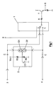
- FIG. 1 shows a preferred embodiment of a circuit schematics of an OSD mixer.
- Fig. 1 shows an OSD mixer with an analogue switch 1, and a clamping circuit 2, which is located between the video signal line 3 and the OSD signal line 4.
- a capacitor C (10 ⁇ F) is provided before the clamping circuit 2 clamps both lines 3, 4 to a common DC level.
- the analogue switch 1 is controlled by a logic control signal 5, which is generated in some logic circuitry (not shown) like a microprocessor.
- the logic signal 5 determines whether the switch of the analogue switch 1 is connected to the video signal line 3 or the OSD signal line 4, which are both input to the analogue switch 1.
- the analogue switch 1 is normally realized as a high speed CMOS analogue switch, like for example the 74HC4053.
- the clamping circuit 2 is realized by a voltage divider consisting of resistors R1 (3.3 kOhms), R2 (3.9 kOhms) wherein R2 is connected to ground and R1 is connected to a supply voltage Vcc (+ 5 V), a capacitor C1 (100 ⁇ F), and two diodes D1, D2 (1SS181).
Landscapes
- Engineering & Computer Science (AREA)
- Computer Graphics (AREA)
- Multimedia (AREA)
- Signal Processing (AREA)
- Picture Signal Circuits (AREA)
- Studio Circuits (AREA)
Applications Claiming Priority (2)
| Application Number | Priority Date | Filing Date | Title |
|---|---|---|---|
| GB9523011A GB2307131A (en) | 1995-11-09 | 1995-11-09 | Mixing osd and video signals with brightness control |
| GB9523011 | 1995-11-09 |
Publications (2)
| Publication Number | Publication Date |
|---|---|
| EP0773675A2 true EP0773675A2 (de) | 1997-05-14 |
| EP0773675A3 EP0773675A3 (de) | 1998-10-21 |
Family
ID=10783676
Family Applications (1)
| Application Number | Title | Priority Date | Filing Date |
|---|---|---|---|
| EP96402329A Withdrawn EP0773675A3 (de) | 1995-11-09 | 1996-10-31 | Schaltung zur Mischung von Video und OSD Signalen |
Country Status (3)
| Country | Link |
|---|---|
| EP (1) | EP0773675A3 (de) |
| JP (1) | JPH09181995A (de) |
| GB (1) | GB2307131A (de) |
Cited By (1)
| Publication number | Priority date | Publication date | Assignee | Title |
|---|---|---|---|---|
| KR100429863B1 (ko) * | 1997-06-24 | 2004-07-19 | 삼성전자주식회사 | 온 스크린 디스플레이 장치 및 방법 |
Family Cites Families (6)
| Publication number | Priority date | Publication date | Assignee | Title |
|---|---|---|---|---|
| US4222073A (en) * | 1977-10-19 | 1980-09-09 | Matsushita Electric Industrial Co., Ltd. | Multiplexed information signal receiving system |
| US4517598A (en) * | 1982-10-22 | 1985-05-14 | George Van Valkenburg | Method and apparatus for electronic publishing |
| US4549217A (en) * | 1983-09-30 | 1985-10-22 | Rca Corporation | Automatic contrast reduction circuit for a teletext or monitor operation |
| JPS60125083A (ja) * | 1983-12-09 | 1985-07-04 | Sharp Corp | 画面表示切換回路 |
| JPS61147677A (ja) * | 1984-12-21 | 1986-07-05 | Mitsumi Electric Co Ltd | ス−パ−インポ−ズ装置 |
| US4663668A (en) * | 1986-06-12 | 1987-05-05 | Rca Corporation | Brightness clamping apparatus for TV receiver with multiple inputs |
-
1995
- 1995-11-09 GB GB9523011A patent/GB2307131A/en not_active Withdrawn
-
1996
- 1996-10-31 EP EP96402329A patent/EP0773675A3/de not_active Withdrawn
- 1996-11-08 JP JP8296353A patent/JPH09181995A/ja active Pending
Non-Patent Citations (1)
| Title |
|---|
| None |
Cited By (1)
| Publication number | Priority date | Publication date | Assignee | Title |
|---|---|---|---|---|
| KR100429863B1 (ko) * | 1997-06-24 | 2004-07-19 | 삼성전자주식회사 | 온 스크린 디스플레이 장치 및 방법 |
Also Published As
| Publication number | Publication date |
|---|---|
| EP0773675A3 (de) | 1998-10-21 |
| JPH09181995A (ja) | 1997-07-11 |
| GB9523011D0 (en) | 1996-01-10 |
| GB2307131A (en) | 1997-05-14 |
Similar Documents
| Publication | Publication Date | Title |
|---|---|---|
| KR960007544B1 (ko) | 모니터에서의 온 스크린 디스플레이 장치 | |
| JPH0235510B2 (de) | ||
| US5343249A (en) | Apparatus for preventing the simultaneous and overlapping display of characters on a television receiver monitor | |
| EP0773675A2 (de) | Schaltung zur Mischung von Video und OSD Signalen | |
| US5499054A (en) | Character and pattern mixing apparatus for use in a video equipment | |
| CN1154037A (zh) | 用于混合视频和屏上显示信号的电路 | |
| KR920007375Y1 (ko) | 온 스크린 문자 번짐 방지회로 | |
| JP3066535B2 (ja) | 子画面出力ブランキング回路 | |
| KR950002703B1 (ko) | 외부입력 절환기능을 구비한 듀얼 애널로그 비디오 포트 | |
| KR840001971Y1 (ko) | 영상 수상기의 동작 표시장치 | |
| KR910003459Y1 (ko) | 문자 혼합회로 | |
| KR960009710Y1 (ko) | 티브이(tv) 동작 설명서의 디스플레이 장치 | |
| KR900006268B1 (ko) | 텔레비젼 수상기의 화면 표시방법 | |
| KR930007446Y1 (ko) | 신호 선택 회로 | |
| KR0149581B1 (ko) | 영상재생장치에서 화면상 표시 문자 흐림 방지회로 | |
| KR890003432Y1 (ko) | 문자표시를 위한 디스플레이 공용회로 | |
| KR900010342Y1 (ko) | 리버스 화이트회로 | |
| KR920002442Y1 (ko) | 세컴 및 메세컴 방식 영상시스템의 osd문자의 색 번짐 방지회로 | |
| JPH0617391Y2 (ja) | テレビジョン受像機 | |
| KR940005992Y1 (ko) | 영상신호 합성 회로 | |
| JPH0454779A (ja) | モニタ付プロジェクタ | |
| KR200158969Y1 (ko) | 모니터의 아날로그 신호와 오에스디신호 믹싱회로 | |
| KR900007856Y1 (ko) | 화면 문자 표시용 출력회로 | |
| KR960012009B1 (ko) | 텔레비젼 수상기의 온-스크린 디스플레이 안정화 회로 | |
| JPH0355995Y2 (de) |
Legal Events
| Date | Code | Title | Description |
|---|---|---|---|
| PUAI | Public reference made under article 153(3) epc to a published international application that has entered the european phase |
Free format text: ORIGINAL CODE: 0009012 |
|
| AK | Designated contracting states |
Kind code of ref document: A2 Designated state(s): DE FR GB IT |
|
| RAP1 | Party data changed (applicant data changed or rights of an application transferred) |
Owner name: THOMSON MULTIMEDIA |
|
| PUAL | Search report despatched |
Free format text: ORIGINAL CODE: 0009013 |
|
| AK | Designated contracting states |
Kind code of ref document: A3 Designated state(s): DE FR GB IT |
|
| 17P | Request for examination filed |
Effective date: 19990419 |
|
| STAA | Information on the status of an ep patent application or granted ep patent |
Free format text: STATUS: THE APPLICATION HAS BEEN WITHDRAWN |
|
| 18W | Application withdrawn |
Withdrawal date: 19990803 |