EP0771077B1 - Paralleler Analog-Digital-Umsetzer mit Schwellenwertspannungs-Einstellung - Google Patents
Paralleler Analog-Digital-Umsetzer mit Schwellenwertspannungs-Einstellung Download PDFInfo
- Publication number
- EP0771077B1 EP0771077B1 EP96117194A EP96117194A EP0771077B1 EP 0771077 B1 EP0771077 B1 EP 0771077B1 EP 96117194 A EP96117194 A EP 96117194A EP 96117194 A EP96117194 A EP 96117194A EP 0771077 B1 EP0771077 B1 EP 0771077B1
- Authority
- EP
- European Patent Office
- Prior art keywords
- transistors
- stage
- analog
- digital
- digital converter
- Prior art date
- Legal status (The legal status is an assumption and is not a legal conclusion. Google has not performed a legal analysis and makes no representation as to the accuracy of the status listed.)
- Expired - Lifetime
Links
Images

Classifications
-
- H—ELECTRICITY
- H03—ELECTRONIC CIRCUITRY
- H03M—CODING; DECODING; CODE CONVERSION IN GENERAL
- H03M1/00—Analogue/digital conversion; Digital/analogue conversion
- H03M1/12—Analogue/digital converters
- H03M1/34—Analogue value compared with reference values
- H03M1/36—Analogue value compared with reference values simultaneously only, i.e. parallel type
- H03M1/361—Analogue value compared with reference values simultaneously only, i.e. parallel type having a separate comparator and reference value for each quantisation level, i.e. full flash converter type
Definitions
- DE-A 34 02 653 (Siemens) describes a method for producing doped regions in semiconductor material by means of ion implantation for the production of microelectronic components.
- a mask or resist layer is applied to a semiconductor substrate and the semiconductor substrate is then etched onto the cover layer together with the SiO 2 or silicon nitride resist layer using a suitable “laser chemical etching method” by optical imaging of the blackening structure of a photomask (there figures 2,3,4).
- the photomask produces an intensity distribution of the radiation on the surface of the resist layer, which forms a resist layer with a two-dimensional thickness relief on the semiconductor substrate with the simultaneous action of the etching process (there, tub 26, etching liquid 27).
- a uniformly distributed implantation radiation produces a doping of the semiconductor substrate that penetrates in the depth direction of the semiconductor substrate with a doping gradient corresponding to the course of the thickness profile of the resist layer.
- semiconductors of microelectronics and power semiconductors can be produced, but preferably optoelectric components.
- AD converters i.e. analog technology
- a flash AD converter is accessible to the person skilled in the art from US Pat. No. 5,237,326 (Jeong).
- This AD converter has a number of comparators that were created in a VLSI process. Their different threshold voltages allow the comparator to be set to create full parallel operation.
- the manufacturing process for manufacturing the different threshold voltages is carried out by adapting the geometric values of the channels of the transistors used there, cf. there column 2, in particular lines 30 to 38 and lines 48 to 57.
- Another production process is shown in the publication Walden et al. , "A Deep-Submicrometer Analog-to-Digital Converter Using Focused-Ion-Beam Implants", Solid State Circuits , Volume 25, No. 2, April 1990, pages 562 to 571.
- the focused ion radiation is used there to set different threshold values with comparators and to generate a flash AD converter.
- the AD converter as shown there is manufactured using CMOS / SOS technology.
- the implantation is done by an FIB, cf. there page 1, left column, under "Introduction”. 32 different threshold values were achieved, cf. number VI there under "Conclusion”, page 569. It was possible to avoid using a resistance ladder.
- a parallel analog-digital converter (AD converter) according to the prior art, an analog input voltage is compared via a multiplicity of comparators with a corresponding number of reference voltages.
- the number of comparators required to compare the input voltage with the reference voltages is a function of the resolution of the input signal measuring range. 2 n -1 comparators are required for a resolution of n bits; which accordingly require a correspondingly large chip area in the converter. In practice, therefore, only a limited number of comparators can be provided for a given chip area, so that this limits the resolution and performance of the analog-digital converter or an undesirably large chip area and depending on the resolution of the analog-digital converter Component size leads.
- the invention is therefore based on the object of creating (also: producing) a parallel analog-to-digital converter which provides increased performance and at the same time reduced space and / or space requirements.
- an analog-digital converter with a first stage with at least one first - preferably several - transistor (s), to which an analog input signal is supplied at its control connection and which depends on the size emits a first digital output signal of the analog signal at the output of the first stage.
- the two or more transistors of the first stage have different doping intensities in their channel (N-channel, P-channel), which are implanted simultaneously (in one step) during manufacture. This results in different threshold voltages U T which lead to the formation of different response thresholds of the transistors to the A / D conversion immediately by incorporating the input signal U in to achieve in a Schwellpressivesskaskade the two or more input transistors.
- a second stage with at least one second transistor is provided that the digital at its control connection Output signal of the first stage as the first digital Receives input signal, depending on the size this first input signal at the output of the second stage second digital output signal can be output.
- a third stage connects with at least a third transistor that its control connection as the second digital output signal receives second digital input signal, depending on the size of this second input signal at the output of the third stage an the analog input signal essentially corresponding digital multi-bit output signal can be output.
- the method according to the invention for producing an analog-digital converter for converting an analog input signal into a digital output signal in parallel is characterized by the steps of applying a photoresist layer to the surface of a semiconductor substrate, and exposing the photoresist layer to a radiation intensity profile accordingly a predetermined pixel scanning of an optical gray-tone lithography photomask, the creation of a resist relief in the photoresist layer on the surface of the semiconductor substrate, by developing and etching the exposed photoresist layer, and the implantation of dopants through the resist relief into the semiconductor substrate.
- the "resist relief” is designed so that different levels (heights or thicknesses) of the resist are each assigned to the local location at which a channel of a MOS input transistor of the first level (the A / D converter stage) is provided.
- Different step heights in the resist lead to different implantation doses in the channel (variation of the channel implantation) with the uniform irradiation with ions during the one implantation and thus to the development of differently adjustable threshold voltages U T1 , U T2 , U T3 ... of the AD-converting transistors.
- the analog-digital converter according to the invention carries out the implementation of the analog input signal in several transistors of the first Implementation stage.
- the transistors only need one comparatively small semiconductor substrate area and replace in the sum of those required in conventional construction and input comparators requiring a relatively large substrate area, which are eliminated, so that the production is more compact and powerful parallel direct converter circuits becomes possible.
- An analog-to-digital converter according to claim 2 allows MOS field effect transistors to be used as switches with a switching threshold dependent on the transistor threshold voltage U T to generate digital states.
- An input stage designed according to claims 4, 5 or 6 allows the switching threshold U T of an inverter operating as a comparator to be varied in almost any range in a simple manner.
- the number of available Implementation levels can be predetermined in a simple manner. According to claims 8 and 9 it is achieved that the Input stage downstream digitization levels simple arrangement of similar microelectronic components can be trained so that a manufacture of the whole Analog-to-digital converter with a smaller number of Production steps becomes possible.
- the threshold voltages U T of transistors distributed over the semiconductor substrate can be set in only one lithography and implantation step.
- MOSFET MOS field effect transistor
- a number of MOSFETs corresponding to the number of converter stages provided is connected in parallel and coupled to a complete parallel conversion in one step (flash conversion) with a 1-out-of-n encoder (so-called priority decoder).
- the threshold voltages U Ti of the MOSFETs are set to suitable values by doping the MOSFET channel area using gray tone lithography and subsequent ion implantation in accordance with the generated (locally distributed) resist relief, i.e. by varying the implantation doses of the implant ions in the channel area (for surface-conducting MOSFETs ) and / or by tub implantation.
- the surface concentration in the channel area is increased by implantation using a gray-scale lacquer mask with an implantation transparency between above 0% and set below 100%.
- a mask is used as the gray-tone lithography photomask, the pixel screening of which has a transparency for the implantation between 0% and 100%.
- the implantation step for setting the threshold voltage U T of MOS field-effect transistors arranged in the semiconductor substrate then forms the respective surface concentrations of the channel regions of the MOS field-effect transistors in accordance with a respective local transparency (the locally controlled, predetermined permeability) of the gray-tone lithography photomask.
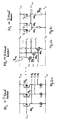
- FIG. 1 (a) shows, for a two-bit converter as an input stage, as an example three P-channel MOS field-effect transistors (MOSFETs) M1 1 , M1 2 and M1 3 forming input transistors arranged in parallel, whose source connections have a first voltage V DD and their drain connections are each connected to a second voltage V SS via a current source I 0 .
- the current source I 0 is also realized by a transistor. This is how a 2-bit converter can be set up.
- An analog input voltage U in to be converted into a digital signal is supplied to the individual gate connections of the MOSFETs M1 1 , M1 2 and M1 3 .
- Output voltages Out 1 , Out 2 and Out 3 are tapped at the drain connections of the MOSFETs M1 1 , M1 2 and M1 3 and coupled to a subsequent second stage of the analog-to-digital converter (ADC).
- ADC analog-to-digital converter
- the input stage of the ADC shown in FIG. 1 (a) forms a parallel arrangement of inverters with a current source load and with different threshold voltages (gray tone lithography comparator) defined in the transistors.
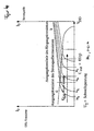
- FIG. 4 shows the profile of the output voltage of an inverter according to FIG. 1 (a) as a function of the threshold voltage U T of the input transistor, with different threshold voltages U T1 , U T2 shown discretely due to different channel doping.
- FIG. 1 (b) shows a 1-out-of-n encoder as an example of the 2-bit ADC from FIG. 1a.
- the respective gate connections of a multiplicity of cascaded N-channel MOSFETs M2 1 , M2 2 and M2 3 (the drain connection of a respective MOSFET is connected to the gate connection of the respective adjacent MOSFET) are the output voltages Out 1 , Out 2 and Out 3 fed.
- the drain connections of the individual N-channel MOSFETs M2 1 , M2 2 and M2 3 are each connected to corresponding resistors R Pu for signal level determination, the other connection of which is coupled to the first voltage V DD .
- Output voltages A 1 , A 2 , A 3 are tapped at the drain connections of the individual N-channel MOSFETs M2 1 , M2 2 and M2 3, which are coupled to the resistors R Pu, and are coupled to a subsequent third stage of the analog-to-digital converter.
- the 1-out-of-n encoder forms a selection means which, depending on the input signals of the encoders Out 1 , Out 2 and Out 3 , sets exactly one of the output signals of the encoders A 1 , A 2 and A 3 to a low level (low).
- FIG. 1 (c) shows the third stage of the analog-digital converter which forms an output stage and which comprises a multiplicity of P-channel MOSFETs M3 1 , M3 2 and M3 3 arranged in parallel, whose source connections have the first voltage V DD and their drain connections are each connected to the second voltage V SS via a resistor R PD .
- the gate connections of the MOSFETs M3 1 , M3 2 and M3 3 are coupled to the outputs A 1 , A 2 and A 3 of the encoder stage.
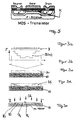
- FIG. 3 (a) to (d) show in simplified form a method in which a photoresist layer, for example a positive resist, is exposed by means of gray-tone photolithography, and can be seen in connection with FIG. 5 , which is a MOS transistor with a channel K shows.
- a photoresist layer for example a positive resist
- a gray value is represented on the photomask 9 by a plurality of white or black pixels, the pixel density and / or pixel size of which varies and thus produces a rasterization of the photomask given by the distribution of the pixels.
- Each screening area is assigned to a channel K of a transistor.
- the shade of gray lithography allows production of a parallel, a transistor threshold voltage cascade having analog-digital converter in a very compact Circuitry. Studies have shown that the circuit arrangement of such an analog-to-digital converter only about 20% of the area of the circuit arrangement one conventional parallel analog-to-digital converter required.
- FIG. 4 should be considered in conjunction with Figure 5 .
- the MOS transistor according to FIG. 5 has a channel region K between the drain and the source connection.
- the forward resistance of the channel is controlled by the voltage at the gate, opposite the D connection or opposite the S connection, depending on the channel doping (N-channel or P-channel).
- N-channel or P-channel the channel doping
- FIG. 4 It can be seen from the characteristic curves in FIG. 4 that a different threshold voltage of a transistor causes a different beginning of the conduction of the channel and the flow of current between drain and source. As the threshold voltage increases due to different channel doping (variation of the implantation dose of the channel), the linear saturation section of the characteristic curve is also shifted to the right and down. Together with a current source according to FIG. 1 (a) or according to FIG.
- the MOS transistors work with different threshold voltages according to FIG. 4 as comparators, the current of the current source being dimensioned such that behind the transition region the working point for the saturation range (in the saturation range).
- the circuits according to FIG. 1 (a) and according to FIG. 2 (a) thus work as comparators, the comparator threshold being determined by the threshold voltage of the MOS transistor.
- FIGS. 2 (a) to 2 (c) are comparable in their function to the circuits according to FIGS. 1 (a) to 1 (c) . Only other types of MOS transistors are used here, with the exception of the respective partial figure (a), which in each case uses a P-channel MOSFET.
- the output signals of the respective sub-figure (a) are staggered so that those outputs, which are coupled to input transistors M1 i , which have a threshold voltage above the difference between VDD and U in , are set to the potential of VSS by their non-conduction. All other outputs are set to the potential VDD and from this output signal configuration the circuit according to sub-figure (b) in FIGS. 1 and 2 converts to only one output with a high or low digital value, all other outputs of the respective sub-figure (b ) are at the other potential.
- the circuit in FIG. 2 (b) is constructed with P-channel transistors, while FIG. 1 (b) was constructed with N-channel transistors. The only difference is that the resistors R PU according to FIG. 1 (b) are switched into resistors R PD to the other potential VSS.
- the circuit according to FIG. 2 (c) is designed in such a way that the one logically active level of the three exemplary output signals from FIG. 2 (b) leads to the corresponding binary word being produced at the two output connections of the two-bit converter.
- the assignments of the output signals of FIG. 2 (b) to the gate connections of FIG. 2 (c) can be clearly seen by naming. If multi-bit output signals are used, correspondingly more transistors M3 1 , M3 2 etc. are connected in parallel, which are connected with their gate connections to the output connections of FIG. 2 (b) in such a way that the number of discrete digital stages of FIG. b) be converted to a binary word.
- FIG. 3 it should also be noted that it relates to the implantation with respect to FIGS. 2 (a) and 1 (a) to the transistors M1 i there .
- a resist layer 20 is applied to this substrate 10 and is exposed to the intensity profile I (x, y).
- a locally changed resist residual height is formed in the profiled resist 21, each residual height being assigned to a channel K i of a MOS transistor to be formed in the input stage of FIG. 1 (a) or FIG. 2 (a).
- the direct juxtaposition of the steps of the resist relief 21 serves to clarify the different heights that would have been no longer so clearly recognizable when spaced apart and associated with a respective transistor.
- FIG. 3 (e) does not indicate the removal of the substrate 10 at the differently masked “steps” K i , but rather indicates the different doping intensity, represented by a penetration of the implantation radiation into the substrate 10 of different depths. This illustration was chosen for reasons of illustration It does not describe that the channels of the MOS transistors to be formed are of different depths, widths or geometrically different designs, rather they are only designed differently in terms of their implantation dose to form different threshold voltages.
Landscapes
- Engineering & Computer Science (AREA)
- Theoretical Computer Science (AREA)
- Analogue/Digital Conversion (AREA)
Description
- Figuren 1 (a) bis (c)
- zeigen vereinfacht eine erste, eine zweite und eine dritte Stufe eines erfindungsgemäßen Analog-Digital-Umsetzers zum parallelen Umsetzen eines analogen Eingangssignals Uin in ein digitales Ausgangssignal Outbit.
- Figuren 2 (a) bis (c)
- zeigen einen alternativen Aufbau eines 2-Bit-AD-Wandlers.
- Figuren 3 (a) bis (e)
- zeigen abstrahiert ein Verfahren zur Belichtung einer auf ein Halbleitersubstrat 10 aufgebrachten Photoresistschicht 20 mittels der Grauton-Photolithographie und zur Erzeugung eines "Implantationsreliefs" 21 auf dem Halbleitersubstrat 10, wobei die verschiedenen Reliefstufen im tatsächlichen Prozess der AD-Wandler-Herstellung nicht nebeneinander, sondern jeweils einem Kanal K1,K2,Ki eines der Eingangstransistoren M11,M12,M13 ... M1i zugeordnet sind. Die Darstellung der Figur 4 soll den Unterschied der Stufenhöhen im Relief verdeutlichen, der zu unterschiedlichen Implantationsdosen in den jeweiligen Kanälen führt.
- Figur 4
- zeigt den Verlauf der Ausgangsspannung eines von der ersten Stufe nach Fig. 1 (a) oder Fig. 2 (a) umfaßten Inverters als Funktion der verschieden gewählten Schwellenspannung UT1,UT2,UT3 ... UTi.
- Figur 5
- ist ein - an sich bekannter - Aufbau eines MOS-Transistors mit Kanal K.
Claims (12)
- Analog-Digital-Umsetzer zum parallelen oder sofortigen Umsetzen eines analogen Eingangssignals (Uin) in ein digitales Ausgangssignal, mitwobei alle Transistoren der ersten Stufe als MOS-Feldeffekttransistoren mit einer jeweils vorbestimmten, unterschiedlichen Schwellenspannung (UT) ausgebildet sind; dadurch gekennzeichnet, daß die Schwellenspannungen (UT) bei der Herstellung im wesentlichen gleichzeitig durch eine Grautonlithographie-Photomaske vorgegeben worden sind, wobei Dotierungen der Kanäle der MOS-Feldeffekttransistoren nicht gleich sind bzw. zwei oder mehr Transistoren der ersten Stufe unterschiedliche Dotierungsintensitäten in ihren Kanälen haben.einer ersten Stufe mit mehreren ersten Transistoren (M11,M12,M13 ...M1i), deren Steueranschlüssen ein analoges Eingangssignal (Uin) zuführbar ist, wobei in Abhängigkeit von der Größe des analogen Eingangssignals am Ausgang (Out1, Out2 ...) der ersten Stufe ein erstes digitales Ausgangssignal abgebbar ist;einer zweiten Stufe mit mehreren zweiten Transistoren (M21,M22,M23 ...M2i), um an Steueranschlüssen das digitale Ausgangssignal der ersten Stufe als erstes digitales Eingangssignal zu empfangen, wobei in Abhängigkeit von der Größe dieses ersten Eingangssignals an einem Ausgang (A1,A2,A3 ...Ai) der zweiten Stufe ein zweites digitales Ausgangssignal abgebbar ist;einer dritten Stufe mit mehreren dritten Transistoren (M31,M32,M33 ... M3i), um an Steueranschlüssen das zweite digitale Ausgangssignal als zweites digitales Eingangssignal zu empfangen, wobei in Abhängigkeit von der Größe dieses zweiten Eingangssignals am Ausgang (Outbit) der dritten Stufe ein dem analogen Eingangssignal entsprechendes digitales Ausgangssignal gebildet und abgebar ist;
- Analog-Digital-Umsetzer nach Anspruch 1, wobei ein Implantationsschritt zur Einstellung der Schwellenspannungen (UT) von in dem Halbleitersubstrat angeordneten MOS-Feldeffekttransistoren die Oberflächenkonzentrationen ihrer Kanalbereiche in Übereinstimmung mit einer jeweiligen örtlich definierten Transparenz der Grautonlithographie-Photomaske erzeugt hat.
- Analog-Digital-Umsetzer nach Anspruch 1 oder 2, dadurch gekennzeichnet, daß die ersten Transistoren (M1i) P-Kanal Enhancement Mode MOS-Feldeffekttransistoren, daß die zweiten Transistoren (M2i) N-Kanal Enhancement Mode MOS-Feldeffekttransistoren, und daß die dritten Transistoren (M3i) P-Kanal Enhancement Mode Feldeffekttransistoren sind, oder vice versa hinsichtlich der zweiten und dritten Stufe.
- Analog-Digital-Umsetzer nach einem der Ansprüche 1 bis 3, dadurch gekennzeichnet, daß die ersten Transistoren an ihren Source-Anschlüssen mit einer ersten Spannung (VDD) und an ihren Drain-Anschlüssen mit jeweils einem Ausgangsanschluß und jeweils einer Stromquelle (I0) zu einer zweiten Spannung (VSS) verbunden sind, wobei das analoge Eingangssignal (Uin) den Gate-Anschlüssen der ersten Transistoren zuführbar ist.
- Analog-Digital-Umsetzer nach Anspruch 4, dadurch gekennzeichnet, daß die jeweilige Stromquelle (I0) einen Transistor mit vorbestimmter Schwellenspannung umfaßt, die auch mittels im Durchlaßverhalten gesteuert veränderter Maske im selben Belichtungs- und Implantationsschritt gebildet wurde, wie die Kanäle der ersten Transistoren (M1i) der ersten Stufe.
- Analog-Digital-Umsetzer nach Anspruch 5, dadurch gekennzeichnet, daß ein jeweiliger erster Transistor und die zugehörige Stromquelle einen Inverter bilden, dessen erste Schaltschwelle (UT) in Abhängigkeit von der Schwellenspannung des ersten Transistors und/oder des zugehörigen Stromquellentransistors festgelegt ist, wobei weitere erste Transistoren (M1i) andere Schwellen-Spannungen (UTi) als der erste Transistor aufweisen.
- Analog-Digital-Umsetzer nach einem der Ansprüche 1 bis 6, wobei die erste Stufe die Vielzahl von parallel angeordneten ersten Transistoren (M11, M12, M13) umfaßt, die zweite Stufe die Vielzahl von in Kaskadenschaltung angeordneten zweiten Transistoren (M21, M22, M23) umfaßt, und die dritte Stufe die Vielzahl von parallel angeordneten dritten Transistoren (M31, M32, M33) umfaßt.
- Analog-Digital-Umsetzer nach Anspruch 1 oder 7, dadurch gekennzeichnet, daß die zweite Stufe als 1-aus-n-Encoder ausgebildet, um in Abhängigkeit von den Pegeln einer Vielzahl von zugeführten ersten digitalen Bits des digitalen Eingangssignals genau einen Ausgangsanschluß (A) auf einen hohen oder niedrigen Pegel zu schalten.
- Analog-Digital-Umsetzer nach Anspruch 1, 7 oder 8, dadurch gekennzeichnet, daß in der dritten Stufe zur Ausgabe eines mit mehreren Bits versehenen binär codierten digitalen Ausgangssignals des Analog-Digital-Umsetzers eine Vielzahl paralleler Ausgangsleitungen (Outbit) in Abhängigkeit von dem genau einen Ausgangs-Anschluß auf hohen bzw. niedrigen Pegel schaltbar sind.
- Verfahren zur Herstellung eines Analog-Digital-Umsetzers zum parallelen Umsetzen eines analogen Eingangssignals in ein digitales Ausgangssignal, gekennzeichnet durch die Schritte(a) Aufbringen einer Photoresistschicht (20) auf die Oberfläche eines Halbleitersubstrats (10);(b) Belichten der Photoresistschicht mit einem Strahlungs-Intensitätsprofil entsprechend einer vorbestimmten Bildpunkt-Rasterung einer optischen Grautonlithographie-Photomaske (9) jeweils an den Orten der Kanäle (Ki) der zu bildenden Transistoren (M1i);(c) Erzeugen eines lokal auf die Orte der jeweiligen Kanäle (Ki) der zu bildenden Transistoren (M1i) ausgerichteten Resistreliefs (21) in der Photoresistschicht (20) durch Entwickeln und/oder Ätzen der belichteten Photoresistschicht;(d) lokal unterschiedliches Implantieren von Dotierungsstoffen durch das Resistrelief hindurch in die Kanalbereiche des Halbleitersubstrats (10), trotz gleichmäßiger Implantatstrahlung auf die Resistschicht (21), so daß die Dotieringen für eine Ausbildung von Schwellenspannungen (UT) der zu bilden den Transistoren im wesentlichen gleichzeitig durch die Grautonlithographie-Photomaske vorgegeben werden.
- Verfahren nach Anspruch 10, dadurch gekennzeichnet, daß als Grautonlithographie-Photomaske eine Maske verwendet wird, deren Bildpunkt-Rasterung eine Transparenz für die Einstellung der lokalen Durchlässigkeit zwischen 0% und 100% aufweist (unter 100%, über 0%).
- Verfahren nach Anspruch 11, dadurch gekennzeichnet, daß der Implantationsschritt gemäß (d) zur Einstellung der Schwellenspannung (UT) von in dem Halbleitersubstrat angeordneten MOS-Feldeffekttransistoren die Oberflächenkonzentrationen ihrer Kanalbereiche in Übereinstimmung mit einer jeweiligen örtlich definierten Transparenz der Grautonlithographie-Photomaske erzeugt.
Applications Claiming Priority (2)
| Application Number | Priority Date | Filing Date | Title |
|---|---|---|---|
| DE19540153 | 1995-10-27 | ||
| DE19540153 | 1995-10-27 |
Publications (3)
| Publication Number | Publication Date |
|---|---|
| EP0771077A2 EP0771077A2 (de) | 1997-05-02 |
| EP0771077A3 EP0771077A3 (de) | 1998-05-20 |
| EP0771077B1 true EP0771077B1 (de) | 2004-07-28 |
Family
ID=7776009
Family Applications (1)
| Application Number | Title | Priority Date | Filing Date |
|---|---|---|---|
| EP96117194A Expired - Lifetime EP0771077B1 (de) | 1995-10-27 | 1996-10-25 | Paralleler Analog-Digital-Umsetzer mit Schwellenwertspannungs-Einstellung |
Country Status (3)
| Country | Link |
|---|---|
| EP (1) | EP0771077B1 (de) |
| AT (1) | ATE272269T1 (de) |
| DE (1) | DE59611045D1 (de) |
Families Citing this family (1)
| Publication number | Priority date | Publication date | Assignee | Title |
|---|---|---|---|---|
| DE19819867C2 (de) * | 1997-05-02 | 2003-04-24 | Fraunhofer Ges Forschung | Verfahren zur Herstellung einer digitalen Gatterschaltung mit herabgesetztem Querstrom |
Family Cites Families (3)
| Publication number | Priority date | Publication date | Assignee | Title |
|---|---|---|---|---|
| US4420743A (en) * | 1980-02-11 | 1983-12-13 | Rca Corporation | Voltage comparator using unequal gate width FET's |
| DE3402653A1 (de) * | 1984-01-26 | 1985-08-01 | Siemens AG, 1000 Berlin und 8000 München | Verfahren zur herstellung speziell dotierter bereiche in halbleitermaterial |
| US5237326A (en) * | 1989-02-02 | 1993-08-17 | Samsung Electronics Co., Ltd. | Flash type analog-to-digital converter having MOS comparators |
-
1996
- 1996-10-25 EP EP96117194A patent/EP0771077B1/de not_active Expired - Lifetime
- 1996-10-25 DE DE59611045T patent/DE59611045D1/de not_active Expired - Lifetime
- 1996-10-25 AT AT96117194T patent/ATE272269T1/de active
Also Published As
| Publication number | Publication date |
|---|---|
| EP0771077A2 (de) | 1997-05-02 |
| DE59611045D1 (de) | 2004-09-02 |
| EP0771077A3 (de) | 1998-05-20 |
| ATE272269T1 (de) | 2004-08-15 |
Similar Documents
| Publication | Publication Date | Title |
|---|---|---|
| EP0006167B1 (de) | Mehrwertiger FET-Festwertspeicher | |
| DE3878559T2 (de) | Analog/digital-umwandler, hergestellt nach der ionenstrahltechnologie. | |
| DE68910740T2 (de) | Pegelumsetzungsschaltung zur Erzeugung eines Signals mit gesteuertem logischen Pegel. | |
| DE2833218A1 (de) | Festkoerper-abbildungsvorrichtung | |
| DE1572374A1 (de) | Elektrophotographisches Aufzeichnungsmaterial | |
| DE2837315A1 (de) | Verfahren zur aenderung der leitfaehigkeit einer halbleiterschicht in einem halbleiterkoerper | |
| DE2047672A1 (de) | Hochfrequenz Feldeffekttransistor | |
| DE1537966A1 (de) | Digital-Analog-Umwandler | |
| EP0010149B1 (de) | Referenzquelle auf einem integrierten FET-Baustein sowie Verfahren zum Betrieb der Referenzquelle | |
| DE2831522A1 (de) | Integrierte schaltung und verfahren zu deren herstellung | |
| DE4420409B4 (de) | Photomaske mit Mustern zur Verringerung der erforderlichen Lichtleistung eines Steppers | |
| EP0157926A1 (de) | Verfahren zum Herstellen einer hochintegrierten MOS-Feld-effekttransistorschaltung | |
| DE3315155A1 (de) | Bildsensor | |
| DE3104210A1 (de) | Umsetzer | |
| DE60124812T2 (de) | Analog-Digital-Wandler nach dem Parallelverfahren | |
| EP0771077B1 (de) | Paralleler Analog-Digital-Umsetzer mit Schwellenwertspannungs-Einstellung | |
| DE19644450B4 (de) | Digitalisierende Eingangsstufe eines AD-Direktumsetzers und Herstellverfahren | |
| DE3009042A1 (de) | Halbleiterwiderstand | |
| EP3637157B1 (de) | Gitterstruktur für eine diffraktive optik | |
| DE2738641A1 (de) | Integrierte halbleiterschaltung | |
| DE10060159A1 (de) | Analog-Digital-Wandler und Verfahren zur Wandlung eines Analogsignals in ein Digitalsignal | |
| DE69712753T2 (de) | Mehrwertiger FET-Festwertspeicher mit einem Substratspannungsgenerator | |
| DE19825043B4 (de) | Maske für die Herstellung integrierter Schaltungen | |
| DE19819867C2 (de) | Verfahren zur Herstellung einer digitalen Gatterschaltung mit herabgesetztem Querstrom | |
| DE19700983C2 (de) | Digital/Analog-Umsetzer |
Legal Events
| Date | Code | Title | Description |
|---|---|---|---|
| PUAI | Public reference made under article 153(3) epc to a published international application that has entered the european phase |
Free format text: ORIGINAL CODE: 0009012 |
|
| AK | Designated contracting states |
Kind code of ref document: A2 Designated state(s): AT BE CH DE FR GB IT LI NL SE |
|
| RIN1 | Information on inventor provided before grant (corrected) |
Inventor name: EICHHOLZ, JOERG Inventor name: QUENZER, HANS JOACHIM Inventor name: STAUDT-FISCHBACH, PETER |
|
| PUAL | Search report despatched |
Free format text: ORIGINAL CODE: 0009013 |
|
| AK | Designated contracting states |
Kind code of ref document: A3 Designated state(s): AT BE CH DE FR GB IT LI NL SE |
|
| 17P | Request for examination filed |
Effective date: 19981120 |
|
| 17Q | First examination report despatched |
Effective date: 20020415 |
|
| RAP1 | Party data changed (applicant data changed or rights of an application transferred) |
Owner name: FRAUNHOFER-GESELLSCHAFT ZUR FOERDERUNG DERANGEWAND |
|
| GRAP | Despatch of communication of intention to grant a patent |
Free format text: ORIGINAL CODE: EPIDOSNIGR1 |
|
| GRAS | Grant fee paid |
Free format text: ORIGINAL CODE: EPIDOSNIGR3 |
|
| GRAA | (expected) grant |
Free format text: ORIGINAL CODE: 0009210 |
|
| AK | Designated contracting states |
Kind code of ref document: B1 Designated state(s): AT BE CH DE FR GB IT LI NL SE |
|
| REG | Reference to a national code |
Ref country code: GB Ref legal event code: FG4D Free format text: NOT ENGLISH |
|
| REG | Reference to a national code |
Ref country code: CH Ref legal event code: EP |
|
| REF | Corresponds to: |
Ref document number: 59611045 Country of ref document: DE Date of ref document: 20040902 Kind code of ref document: P |
|
| REG | Reference to a national code |
Ref country code: CH Ref legal event code: NV Representative=s name: KELLER & PARTNER PATENTANWAELTE AG |
|
| REG | Reference to a national code |
Ref country code: SE Ref legal event code: TRGR |
|
| GBT | Gb: translation of ep patent filed (gb section 77(6)(a)/1977) |
Effective date: 20041111 |
|
| ET | Fr: translation filed | ||
| PLBE | No opposition filed within time limit |
Free format text: ORIGINAL CODE: 0009261 |
|
| STAA | Information on the status of an ep patent application or granted ep patent |
Free format text: STATUS: NO OPPOSITION FILED WITHIN TIME LIMIT |
|
| 26N | No opposition filed |
Effective date: 20050429 |
|
| REG | Reference to a national code |
Ref country code: CH Ref legal event code: PCAR Free format text: NEW ADDRESS: EIGERSTRASSE 2 POSTFACH, 3000 BERN 14 (CH) |
|
| REG | Reference to a national code |
Ref country code: FR Ref legal event code: PLFP Year of fee payment: 20 |
|
| PGFP | Annual fee paid to national office [announced via postgrant information from national office to epo] |
Ref country code: GB Payment date: 20151026 Year of fee payment: 20 Ref country code: IT Payment date: 20151026 Year of fee payment: 20 Ref country code: CH Payment date: 20151026 Year of fee payment: 20 Ref country code: DE Payment date: 20151022 Year of fee payment: 20 |
|
| PGFP | Annual fee paid to national office [announced via postgrant information from national office to epo] |
Ref country code: BE Payment date: 20151022 Year of fee payment: 20 Ref country code: NL Payment date: 20151026 Year of fee payment: 20 Ref country code: AT Payment date: 20151022 Year of fee payment: 20 Ref country code: FR Payment date: 20151026 Year of fee payment: 20 Ref country code: SE Payment date: 20151026 Year of fee payment: 20 |
|
| REG | Reference to a national code |
Ref country code: DE Ref legal event code: R071 Ref document number: 59611045 Country of ref document: DE |
|
| REG | Reference to a national code |
Ref country code: NL Ref legal event code: MK Effective date: 20161024 |
|
| REG | Reference to a national code |
Ref country code: CH Ref legal event code: PL |
|
| REG | Reference to a national code |
Ref country code: GB Ref legal event code: PE20 Expiry date: 20161024 |
|
| REG | Reference to a national code |
Ref country code: SE Ref legal event code: EUG |
|
| REG | Reference to a national code |
Ref country code: AT Ref legal event code: MK07 Ref document number: 272269 Country of ref document: AT Kind code of ref document: T Effective date: 20161025 |
|
| PG25 | Lapsed in a contracting state [announced via postgrant information from national office to epo] |
Ref country code: GB Free format text: LAPSE BECAUSE OF EXPIRATION OF PROTECTION Effective date: 20161024 |