EP0768783A2 - Adaptive Symbolrückgewinnung für APSK-Signale - Google Patents
Adaptive Symbolrückgewinnung für APSK-Signale Download PDFInfo
- Publication number
- EP0768783A2 EP0768783A2 EP96307251A EP96307251A EP0768783A2 EP 0768783 A2 EP0768783 A2 EP 0768783A2 EP 96307251 A EP96307251 A EP 96307251A EP 96307251 A EP96307251 A EP 96307251A EP 0768783 A2 EP0768783 A2 EP 0768783A2
- Authority
- EP
- European Patent Office
- Prior art keywords
- bit
- keyed
- amplitude
- bang
- digital
- Prior art date
- Legal status (The legal status is an assumption and is not a legal conclusion. Google has not performed a legal analysis and makes no representation as to the accuracy of the status listed.)
- Withdrawn
Links
- 238000011084 recovery Methods 0.000 title claims abstract description 51
- 230000003044 adaptive effect Effects 0.000 title claims abstract description 10
- 238000004891 communication Methods 0.000 claims abstract description 22
- 238000012545 processing Methods 0.000 claims abstract description 6
- 230000004044 response Effects 0.000 claims abstract description 6
- 238000001514 detection method Methods 0.000 claims description 13
- 238000013459 approach Methods 0.000 claims description 2
- 238000000034 method Methods 0.000 abstract description 9
- 230000001427 coherent effect Effects 0.000 description 3
- 238000012544 monitoring process Methods 0.000 description 3
- 238000000926 separation method Methods 0.000 description 1
- 230000001629 suppression Effects 0.000 description 1
Images

Classifications
-
- H—ELECTRICITY
- H04—ELECTRIC COMMUNICATION TECHNIQUE
- H04L—TRANSMISSION OF DIGITAL INFORMATION, e.g. TELEGRAPHIC COMMUNICATION
- H04L27/00—Modulated-carrier systems
- H04L27/02—Amplitude-modulated carrier systems, e.g. using on-off keying; Single sideband or vestigial sideband modulation
-
- H—ELECTRICITY
- H04—ELECTRIC COMMUNICATION TECHNIQUE
- H04L—TRANSMISSION OF DIGITAL INFORMATION, e.g. TELEGRAPHIC COMMUNICATION
- H04L25/00—Baseband systems
- H04L25/02—Details ; arrangements for supplying electrical power along data transmission lines
- H04L25/06—DC level restoring means; Bias distortion correction ; Decision circuits providing symbol by symbol detection
- H04L25/068—DC level restoring means; Bias distortion correction ; Decision circuits providing symbol by symbol detection by sampling faster than the nominal bit rate
-
- H—ELECTRICITY
- H04—ELECTRIC COMMUNICATION TECHNIQUE
- H04L—TRANSMISSION OF DIGITAL INFORMATION, e.g. TELEGRAPHIC COMMUNICATION
- H04L27/00—Modulated-carrier systems
- H04L27/32—Carrier systems characterised by combinations of two or more of the types covered by groups H04L27/02, H04L27/10, H04L27/18 or H04L27/26
- H04L27/34—Amplitude- and phase-modulated carrier systems, e.g. quadrature-amplitude modulated carrier systems
- H04L27/38—Demodulator circuits; Receiver circuits
- H04L27/3818—Demodulator circuits; Receiver circuits using coherent demodulation, i.e. using one or more nominally phase synchronous carriers
- H04L27/3827—Demodulator circuits; Receiver circuits using coherent demodulation, i.e. using one or more nominally phase synchronous carriers in which the carrier is recovered using only the demodulated baseband signals
Definitions
- the present invention relates to amplitude phased keyed communications systems, and more particularly to an improved amplitude phased keyed digital symbol recovery circuit for use in an amplitude phased keyed digital communications system.
- adaptive digital symbol recovery is performed by analog threshold processing of I and Q baseband signals. Any signal can be decomposed into orthogonal signals comprising in-phase (I) and quadrature (Q) signals.
- I in-phase
- Q quadrature
- amplitude phase keyed (APK) communications signals the transmitted symbols are typically recovered via sum and difference circuits operating, on the orthogonal signals at baseband. With the knowledge of the amplitude of each of the signals at the correct sample times, amplitude phase keyed symbols can be recovered.
- conventional communication systems are not expandable nor programmable. Conventional communication systems typically do not process a very wide variety of signal constellations and cannot be programmed to process new signal constellations using only a memory upload sequence.
- False lock detection is conventionally done by monitoring the bit error rate of the system. which typically involves the use of added circuitry. Therefore, false lock detection is relatively complex and costly to implement.
- Carrier lock status is conventionally implemented using a complex circuit configuration, and is also relatively costly to implement.
- the present invention seeks to provide for an amplitude phased keyed digital communications system having an improved digital symbol recovery circuit.
- the present invention may permit the provision of an amplitude phased keyed digital communications system having an improved digital symbol recovery circuit that is programmable and expandable and that provides a means for cost-effectively implementing carrier tracking and recovery and false lock detection, automatic gain control and that is capable of processing a wide variety of signal constellations using only a memory upload sequence to adapt to the new signal constellation.
- a digital symbol recovery circuit for a digital communications system, the circuit comprising a programmable addressable random access memory coupled to the adaptive baseband equalizer for storing a plurality of eight bit words comprising decoded symbol sets of the received amplitude phased keyed signals, and for outputting the decoded symbol sets in response to addresses corresponding to the in-phase and quadrature output signals received thereby and a quadrature demodulator coupled to the digital symbol recovery circuit for processing the decoded symbol sets and for outputting recovered amplitude phased keyed symbols corresponding to the received amplitude phased keyed signals in response thereto.
- the present invention permits improvements to amplitude phased keyed (APK) digital communications systems and to the processing of amplitude phase keyed symbols transmitted over radio frequency channels.
- the adaptive baseband equalizer can be arranged to receive amplitude phased keyed signals and provide outputs in-phase (I) and quadrature (Q) digital amplitude values corresponding to the received amplitude-phased keyed (APK) signals.
- the digital symbol recovery circuit may store a plurality of eight bit words comprising decoded symbol sets of the received amplitude phased keyed signals, and output the decoded symbol sets in response to addresses corresponding to the I and Q output signals.
- the quadrature demodulator processes the received passband symbols and output digital words representing recovered APK I and Q baseband signals corresponding to the received amplitude phased keyed symbols in the radio frequency (RF) channel.
- RF radio frequency
- the I and Q signals may be sampled at the symbol centers and then quantized.
- the digital amplitudes of the I and Q signals are input to a digital symbol recovery circuit.
- the digital symbol recovery circuit is programmable and adaptable to channel distortions, providing programmable adaptable decision regions that optimize symbol recovery and minimize bit error rates.
- the digital symbol recovery circuit processes digital (quantized) versions of the analog I and Q component signal voltages
- the digital symbol recovery decision regions and thresholds of separation may be fully programmable (memory uploadable).
- the digital symbol recovery decision boundaries can be adaptable to conform to the distortion characteristics of a given communications channel.
- the digital symbol recovery circuit may support digital automatic phase control (APC) boundary decisions for carrier recovery, digital automated gain control (AGC), and digital false lock detection data.
- APC digital automatic phase control
- APC digital automated gain control
- the fully programmable symbol recovery circuit may be used to process any of a large class of APK signals and can be optimized for the distortions of a given channel.
- a refinement of the present invention is that, for each symbol received, the digital symbol recovery circuit outputs a 1-bit quantized (bang-bang) phase error bit to a quadrature demodulator indicating whether the phase of the received signal is ahead of or lagging the estimated phase.
- This programmable capability drives a bang-bang phase lock loop in the quadrature demodulator to provide coherent carrier tracking and recovery.
- the circuit processes multiple amplitude signals as well as constant envelope signals.
- AGC false-lock signals may be provided as output signals therefrom by means of a simple and highly accurate implementation of the digital symbol recovery circuit. False lock detection is conventionally done by monitoring the bit error rate of the communication system.
- Another refinement of the present invention is that, if the bang-bang phase lock loop is in false lock, the bang-bang phase bit for certain predeterminable points in the constellation will be predominantly 0's or 1's.
- False lock detection in conjunction with digital symbol recovery provided by the present circuit provides the programmable capability to monitor any selected constellation points and use the bang-bang phase bit to determine false lock. Monitoring a given constellation allows the bang-bang phase bit decision to drive the bang-bang phase lock loop in a direction required to correct the lock state.
- the bang-bang phase lock loop may encounter additional false lock states on the way to the correct lock state, but the process is repeated until the correct lock state is achieved.
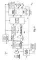
- Figure 1 illustrates an amplitude phased keyed digital symbol recovery circuit 10 in accordance with the principles of the present invention employed with an amplitude phased keyed digital communications system 20.
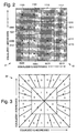
- Figure 2 illustrates a 16 QAM symbol map 21 employed in the digital symbol recovery circuit 10 of Figure 1.
- Figure 3 illustrates a carrier tracking bang-bang servo map 22 employed in the digital symbol recovery circuit 10 of Figure 1.
- Figure 4 illustrates a 16 QAM automatic gain control map 23 employed in the digital symbol recovery circuit 10 of Figure 1.
- Figure 5 illustrates a false lock detection map 24 employed in the digital symbol recovery circuit 10 of Figure 1.
- a portion of the amplitude phased keyed digital communications system 20 is shown in Figure 1 and comprises an adaptive baseband equalizer 11, the present digital symbol recovery circuit 10, and a quadrature demodulator 12.
- the quadrature demodulator 12 comprises an amplifier 31, for receiving amplitude phased keyed signals 13 or symbols 13, a coherent detector 32 comprising a bang-bang phase lock loop 33, a symbol clock recovery circuit 34, I and Q sampler and quantizer circuits 35a, 35b, and an IF gain control circuit 36.
- the IF gain control circuit 36 has a reference voltage applied thereto and a bang-bang phase bit 16 derived from the digital symbol recovery circuit 10.
- the digital symbol recovery circuit 10 is a programmable (memory uploadable) circuit 10 that makes symbol decisions in the 1-Q plane for received signals containing a wide class of amplitude phase keyed (APK) modulations.
- the architecture of the digital symbol recovery circuit 10 comprises a large addressable random access memory 10a (RAM look-up table 10a) whose memory contents are addressed by 8 bit quantized I and Q digital amplitude values 13a of received amplitude phased keyed signals 13 or symbols 13.
- the addressable memory 10a has 256 x 256 (64K) locations (illustrated in Figure 2). Each memory location stores an 8 bit word 25 that contains the decoded symbol "n-tuple" 14 corresponding to the received amplitude phased keyed signals 13.
- 16-ary i.e. 16 QAM
- four bits (4-tuples) define each of 16 possible amplitude phased keyed (APK) symbol states.
- APK amplitude phased keyed
- four bits are read out from the digital symbol recovery circuit 10 (memory 10a) and a symbol decision is made. Additional bits are available for larger APK symbol sets (n-tuples), such as 64 (6-tuples), 256 (8-tuples), 1024 (10-tuples) APK, etc., communications signals.
- This aspect of the present invention provides for expansion of the addressable memory locations in the memory 10a and the size of the digital words 25 stored at each location from 8 bits to a word size required to recover higher order APK signal symbols 13.
- extra bits are available for determining whether the phase sample of a phase tracking coherent detector (not shown) lags or leads the estimated phase state shown in Figure 3.
- This datum facilitates "bang-bang" phase lock loop tracking of the complex APK received sequence and comprises the bang-bang phase bit 15 or automated phase control bit 15 (APC-bit) shown in Figures 1 and 3.
- An additional bit determines whether of the amplitude of the received symbol 13 is greater or smaller than the ideal amplitude of the symbol 13. This is an automatic gain control bit 16 (AGC-bit) shown in Figure 4.
- AGC-bit automatic gain control bit 16
- an additional bit is designated as a "false lock detect” indicator bit 17.
- the false lock detect bit 17 shown in Figure 5 facilitates suppression of false lock modes that are encountered in the bang-bang phase tracking system.
- decision regions for the recovered symbols 13 may be arbitrarily changed.
- the decision regions may be redefined for other APK symbol structures such as 8 PSK. 12, 4 APK, 64 QAM or many others.
- the decision regions in the memory 10a of the digital symbol recovery circuit 10 may be optimized to provide a minimum probability of symbol decision error, by statistically analyzing the received samples in 1-Q space, and thereby adapting system 20 for near optimum performance in a particular distorting channel environment.
- the digital symbol recovery circuit 10 receives digital I and Q amplitude values 13a from an adaptive baseband equalizer 11.
- the 8-bit I and 8-bit Q amplitude values 13a address 256 x 256 memory locations (64K) in the memory 10a of the digital symbol recovery circuit 10.
- a 7 bit word 25 is stored. This may be expanded to larger words for more complex constellations.
- the first four bits define a 4-tuple 14 for the decoded symbol 13. This is only in the instance of 16-ary APK waveforms.
- 3 bits represent the decoded symbol.
- 64-ary 6 bits represent the decoded symbol.
- the fifth bit is the bang-bang phase error bit 15 or carrier tracking bit 15.
- the sixth bit is the bang-bang AGC error bit 16.
- the seventh bit is the false lock indicator bit 17.
- Any signal 13 may be decomposed into orthogonal signals comprising in-phase (I) and quadrature (Q) signals 13a.
- I and Q signals 13 are digitally sampled at centers of the symbol 13a by I and Q sampler and quantizer circuits 35a, 35b, and the digital amplitudes of the I and Q symbols 13 are input to the digital symbol recovery circuit 10.
- the digital symbol recovery circuit 10 outputs the AGC bit 16 to the quadrature demodulator 12 indicating whether the amplitude of the received signal 13 was above or below an ideal amplitude.
- This programmable capability drives an AGC bang-bang circuit (not shown) in the quadrature demodulator 12 to provide highly accurate gain control.
- the bang-bang bit stream (bits 14-18) is low pass filtered in the quadrature demodulator 12 and the bang-bang AGC loop is closed.
- An additional bit (the false lock bit 17) in each memory location is coded with a "0' or a " 1" depending on whether that point in the constellation is to be used as a false lock detection point.
- Figure 3 shows the bang-bang carrier tracking map 22.
- Figure 4 shows the AGC map 23.
- Figure 5 shows the false lock detect map 24.
- the bang-bang phase bits 15 are monitored to determine if there is a predominance of 0's or 1's. If a programmable ratio of 0's or 1's is exceeded, the bang-bang phase locked loop is driven with either 0's or 1's by a programmable distance to approach the correct lock position. If another false lock condition is encountered, the process in repeated until correct lock is achieved.
Landscapes
- Engineering & Computer Science (AREA)
- Computer Networks & Wireless Communication (AREA)
- Signal Processing (AREA)
- Power Engineering (AREA)
- Digital Transmission Methods That Use Modulated Carrier Waves (AREA)
- Cable Transmission Systems, Equalization Of Radio And Reduction Of Echo (AREA)
- Synchronisation In Digital Transmission Systems (AREA)
Applications Claiming Priority (2)
| Application Number | Priority Date | Filing Date | Title |
|---|---|---|---|
| US08/543,814 US5898737A (en) | 1995-10-16 | 1995-10-16 | Adaptive digital symbol recovery for amplitude phased keyed digital communication systems |
| US543814 | 1995-10-16 |
Publications (2)
| Publication Number | Publication Date |
|---|---|
| EP0768783A2 true EP0768783A2 (de) | 1997-04-16 |
| EP0768783A3 EP0768783A3 (de) | 1998-04-01 |
Family
ID=24169650
Family Applications (1)
| Application Number | Title | Priority Date | Filing Date |
|---|---|---|---|
| EP96307251A Withdrawn EP0768783A3 (de) | 1995-10-16 | 1996-10-03 | Adaptive Symbolrückgewinnung für APSK-Signale |
Country Status (11)
| Country | Link |
|---|---|
| US (1) | US5898737A (de) |
| EP (1) | EP0768783A3 (de) |
| JP (1) | JPH09181789A (de) |
| KR (1) | KR970024755A (de) |
| CN (1) | CN1153426C (de) |
| AU (1) | AU720461B2 (de) |
| BR (1) | BR9605144A (de) |
| CA (1) | CA2184306A1 (de) |
| IL (1) | IL119340A (de) |
| SG (1) | SG90014A1 (de) |
| TW (1) | TW333732B (de) |
Cited By (2)
| Publication number | Priority date | Publication date | Assignee | Title |
|---|---|---|---|---|
| WO2001001650A1 (en) * | 1999-06-30 | 2001-01-04 | Harris Corporation | Device and methods for false carrier lock detection in a receiver |
| EP1039712A3 (de) * | 1999-03-25 | 2003-10-22 | SANYO ELECTRIC Co., Ltd. | Vermeidung von Fehlverriegelung in Quadraturdemodulatoren |
Families Citing this family (8)
| Publication number | Priority date | Publication date | Assignee | Title |
|---|---|---|---|---|
| US6614861B1 (en) * | 1999-04-16 | 2003-09-02 | Nokia Networks Oy | Method and apparatus for higher dimensional modulation |
| KR100652028B1 (ko) * | 1999-07-13 | 2006-11-30 | 엘지전자 주식회사 | 다매체 디지털 방송 수신기의 락 디텍트(lock detect)장치 |
| US6373389B1 (en) | 2000-04-21 | 2002-04-16 | Usm Systems, Ltd. | Event driven information system |
| US6812783B2 (en) * | 2001-08-31 | 2004-11-02 | Northrop Grumman Corporation | Discritized phase constellation continuous phase modulation demodulator |
| DE102006030915B4 (de) * | 2006-06-29 | 2008-04-10 | Fraunhofer-Gesellschaft zur Förderung der angewandten Forschung e.V. | Optischer Empfänger für den Empfang eines Signales mit M-wertiger sternförmiger Quadratur-Amplitudenmodulation mit differenzieller Phasenkodierung und dessen Verwendung |
| FR3085568B1 (fr) * | 2018-08-31 | 2020-08-07 | Zodiac Data Systems | Procede de datation de signaux de telemesure |
| CN113189403B (zh) * | 2021-04-12 | 2022-11-25 | 东北大学 | 一种自适应正交解调方法 |
| CN117172163B (zh) * | 2023-08-15 | 2024-04-12 | 重庆西南集成电路设计有限责任公司 | 幅相控制电路的幅相二维优化方法、系统、介质及电子设备 |
Family Cites Families (11)
| Publication number | Priority date | Publication date | Assignee | Title |
|---|---|---|---|---|
| US4546322A (en) * | 1983-08-24 | 1985-10-08 | Reliance Electric Company | Adaptable demodulator for arbitrary amplitude and phase keyed modulation signals |
| US4866395A (en) * | 1988-11-14 | 1989-09-12 | Gte Government Systems Corporation | Universal carrier recovery and data detection for digital communication systems |
| US4987375A (en) * | 1990-02-15 | 1991-01-22 | Northern Telecom Limited | Carrier lock detector for a QAM system |
| FI85548C (fi) * | 1990-06-14 | 1992-04-27 | Nokia Oy Ab | Mottagningsfoerfarande och mottagare foer diskreta signaler. |
| JP2794964B2 (ja) * | 1991-02-27 | 1998-09-10 | 日本電気株式会社 | 制御信号発生回路 |
| AU655384B2 (en) * | 1991-07-26 | 1994-12-15 | General Instrument Corporation | Carrier phase recovery for an adaptive equalizer |
| US5315617A (en) * | 1992-05-29 | 1994-05-24 | General Electric Company | QAM encoding for high-definition television system |
| US5264937A (en) * | 1992-07-29 | 1993-11-23 | Thomson Consumer Electronics, Inc. | Apparatus for time division multiplexed processing of frequency division multiplexed signals |
| US5563916A (en) * | 1995-06-05 | 1996-10-08 | Hitachi America, Ltd. | Apparatus and method for varying the slew rate of a digital automatic gain control circuit |
| US5671253A (en) * | 1995-07-12 | 1997-09-23 | Thomson Consumer Electronics, Inc. | Apparatus for demodulating and decoding video signals encoded in different formats |
| US5809086A (en) * | 1996-03-20 | 1998-09-15 | Lucent Technologies Inc. | Intelligent timing recovery for a broadband adaptive equalizer |
-
1995
- 1995-10-16 US US08/543,814 patent/US5898737A/en not_active Expired - Lifetime
-
1996
- 1996-08-28 CA CA002184306A patent/CA2184306A1/en not_active Abandoned
- 1996-09-23 AU AU65780/96A patent/AU720461B2/en not_active Ceased
- 1996-10-01 IL IL11934096A patent/IL119340A/en not_active IP Right Cessation
- 1996-10-03 EP EP96307251A patent/EP0768783A3/de not_active Withdrawn
- 1996-10-09 TW TW085112379A patent/TW333732B/zh not_active IP Right Cessation
- 1996-10-12 SG SG9610849A patent/SG90014A1/en unknown
- 1996-10-15 JP JP8291225A patent/JPH09181789A/ja active Pending
- 1996-10-15 KR KR1019960046020A patent/KR970024755A/ko not_active Ceased
- 1996-10-15 BR BR9605144A patent/BR9605144A/pt not_active IP Right Cessation
- 1996-10-16 CN CNB961226420A patent/CN1153426C/zh not_active Expired - Fee Related
Cited By (2)
| Publication number | Priority date | Publication date | Assignee | Title |
|---|---|---|---|---|
| EP1039712A3 (de) * | 1999-03-25 | 2003-10-22 | SANYO ELECTRIC Co., Ltd. | Vermeidung von Fehlverriegelung in Quadraturdemodulatoren |
| WO2001001650A1 (en) * | 1999-06-30 | 2001-01-04 | Harris Corporation | Device and methods for false carrier lock detection in a receiver |
Also Published As
| Publication number | Publication date |
|---|---|
| CN1153426C (zh) | 2004-06-09 |
| CN1155800A (zh) | 1997-07-30 |
| AU720461B2 (en) | 2000-06-01 |
| US5898737A (en) | 1999-04-27 |
| KR970024755A (ko) | 1997-05-30 |
| IL119340A (en) | 2001-09-13 |
| IL119340A0 (en) | 1997-01-10 |
| CA2184306A1 (en) | 1997-04-17 |
| SG90014A1 (en) | 2002-07-23 |
| TW333732B (en) | 1998-06-11 |
| BR9605144A (pt) | 1998-07-07 |
| EP0768783A3 (de) | 1998-04-01 |
| JPH09181789A (ja) | 1997-07-11 |
| AU6578096A (en) | 1997-04-24 |
Similar Documents
| Publication | Publication Date | Title |
|---|---|---|
| US5872812A (en) | Carrier reproducing circuit including region deciding circuitry | |
| US4885756A (en) | Method of demodulating digitally modulated signals, and apparatus implementing such a method | |
| US5898737A (en) | Adaptive digital symbol recovery for amplitude phased keyed digital communication systems | |
| US4849991A (en) | Method and circuitry for determining symbol timing for time division multiple access radio systems | |
| WO1998023070A9 (en) | Passband dqpsk detector for a digital communications receiver | |
| JPS61198848A (ja) | デ−タ受信システム | |
| AU2005278238A1 (en) | Method and apparatus for calculating log-likelihood ratio for decoding in a receiver for a mobile communication system | |
| EP0572376B1 (de) | Spektral wirksames digital-fm-modulationssystem | |
| US6038264A (en) | Data receiving apparatus | |
| US5509030A (en) | RF receiver AGC incorporating time domain equalizer circuity | |
| US4647864A (en) | Variable-delay, sine-cosine non-coherent demodulator | |
| JP3691936B2 (ja) | 多値直交振幅変調装置及び多値直交振幅変調方法 | |
| US6973142B2 (en) | Timing synchronization for M-DPSK channels | |
| CA1268222A (en) | Method for recovering a phase difference signal | |
| US6519303B1 (en) | Clock reproduction circuit | |
| JPH04271551A (ja) | 制御信号発生回路 | |
| US5333150A (en) | Demodulation and synchronization method and system for digitally modulated signals | |
| HK1000652A (en) | Adaptive symbol recovery for apsk signals | |
| US4432094A (en) | Method for recognizing digital information transmitted in a mobile radio communication system | |
| US4803385A (en) | Phase detecting circuit | |
| KR20050033863A (ko) | 동기화 방법 및 회로 | |
| EP0785647A1 (de) | Verfahren und Anordnung in einem Empfänger zur Synchronisierung von FSK modulierten Signalen | |
| EP1263162B1 (de) | Einrichtung und Verfahren zur digitalen Demodulation eines Empfangssignals durch Selektion eines Filters und damit hergestellter digitaler Kommunikationsempfänger | |
| CA2552020C (en) | Method and apparatus for wide dynamic range reduction | |
| CN1152976A (zh) | 直接变频接收机 |
Legal Events
| Date | Code | Title | Description |
|---|---|---|---|
| PUAI | Public reference made under article 153(3) epc to a published international application that has entered the european phase |
Free format text: ORIGINAL CODE: 0009012 |
|
| AK | Designated contracting states |
Kind code of ref document: A2 Designated state(s): AT BE CH DE DK ES FI FR GB GR IE IT LI LU MC NL PT SE |
|
| PUAL | Search report despatched |
Free format text: ORIGINAL CODE: 0009013 |
|
| AK | Designated contracting states |
Kind code of ref document: A3 Designated state(s): AT BE CH DE DK ES FI FR GB GR IE IT LI LU MC NL PT SE |
|
| 17P | Request for examination filed |
Effective date: 19980812 |
|
| 17Q | First examination report despatched |
Effective date: 20040216 |
|
| STAA | Information on the status of an ep patent application or granted ep patent |
Free format text: STATUS: THE APPLICATION IS DEEMED TO BE WITHDRAWN |
|
| 18D | Application deemed to be withdrawn |
Effective date: 20040827 |
|
| REG | Reference to a national code |
Ref country code: HK Ref legal event code: WD Ref document number: 1000652 Country of ref document: HK |