EP0762637A2 - Amplificateur à puissance de sortie variable - Google Patents
Amplificateur à puissance de sortie variable Download PDFInfo
- Publication number
- EP0762637A2 EP0762637A2 EP96306236A EP96306236A EP0762637A2 EP 0762637 A2 EP0762637 A2 EP 0762637A2 EP 96306236 A EP96306236 A EP 96306236A EP 96306236 A EP96306236 A EP 96306236A EP 0762637 A2 EP0762637 A2 EP 0762637A2
- Authority
- EP
- European Patent Office
- Prior art keywords
- units
- unit
- variable gain
- power supply
- variable
- Prior art date
- Legal status (The legal status is an assumption and is not a legal conclusion. Google has not performed a legal analysis and makes no representation as to the accuracy of the status listed.)
- Ceased
Links
Images


Classifications
-
- H—ELECTRICITY
- H03—ELECTRONIC CIRCUITRY
- H03G—CONTROL OF AMPLIFICATION
- H03G3/00—Gain control in amplifiers or frequency changers
- H03G3/20—Automatic control
- H03G3/30—Automatic control in amplifiers having semiconductor devices
-
- H—ELECTRICITY
- H03—ELECTRONIC CIRCUITRY
- H03G—CONTROL OF AMPLIFICATION
- H03G3/00—Gain control in amplifiers or frequency changers
- H03G3/004—Control by varying the supply voltage
Definitions
- the present invention relates to a variable output amplifier apparatus which may, for example, be used in a mobile communications transmitter in which, severe restrictions are imposed on power dissipation.
- the level of received signals fluctuates greatly during communications by mobile apparatus.
- the range of the intensity level can be between about 80 dB to 100 dB.
- linear modulation systems and multi-valued transmission systems have been considered.
- the bandwidth occupied is made broad, and the information superposed on the amplitude of the carriers is destroyed.
- a wide range variable output amplifier apparatus is required at both the transmitter and the receiver in such systems.
- a base station in which a plurality of mobile stations use the same frequency band simultaneously, a base station has to receive signals from all of the mobile stations at approximately the same level. That is, if the intensity of a signal from one mobile station is too strong, it is difficult to exclude its effect upon the other mobile stations, which reduces the actual transmission capacity. Thus, a wide range variable output amplifier apparatus is also required at the transmitting side of such a system.
- DS-CDMA direct sequence code division multiple access
- a first previously proposed variable output amplifier apparatus for power transmission (see: JP-A-58-83437), an input signal is amplified by first and second power amplifiers. A part of an output signal from the second power amplifier is fed back by a directional coupler to a detector. The directional coupler also provides an output signal. A control circuit compares the output of the detector with a reference voltage, and as a result, the power supply of the first power amplifier is controlled in accordance with the result of the comparison of the output of the detector with the reference voltage. In addition, when the transmission power is low, a changeover switch is selected, so that the power supply of the second power amplifier is switched to the same power supply for the first power amplifier. This will be explained later in detail.
- a plurality of first amplifiers is connected in parallel for receiving an input signal.
- the first amplifiers are connected via a first changeover switch to a plurality of second amplifiers connected in parallel, the second amplifiers being connected via a second changeover switch to a detector.
- the second changeover switch provides an output signal.
- the output signal of the detector is supplied to a selection determination circuit for controlling the changeover switches. That is, the selection determination circuit selects an optimum combination of one of the first amplifiers and one of the second amplifiers in accordance with the output of the detector. This will also be explained later in detail.
- a feature of an arrangement to be described below and illustrative of the present invention is that a wide range variable output apparatus with a high efficiency is provided.
- an input signal is distributed by a distributing unit as first signals to a plurality of variable gain units having different gains and providing maximum output power.
- Second signals generated by the variable gain units are combined by a combining unit to generate an output signal.
- a plurality of power supply control units supplies power to each of the variable gain units, respectively.
- the variable gain units and the power supply control units are controlled by a control unit. When one of the variable gain units and one of the power supply control units are activated, the corresponding power supply is rapidly turned ON. When they are deactivated, the corresponding power supply is slowly turned OFF.
- variable output amplifier apparatus Before the description is made of the embodiments illustrative of the invention, previously proposed variable output amplifier apparatus will be described with reference to Figs. 1 and 2.
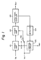
- Fig. 1 which illustrates a first previously proposed variable output amplifier apparatus for power transmission (see: JP-A-58-83437)
- an input signal S IN is amplified by power amplifiers 101 and 102.
- a part of an output signal of the power amplifiers 102 is fed back by a directional coupler 103 to a detector 104.
- the directional coupler 103 also feeds an output signal S OUT .
- a control circuit 105 compares a transmission power level detected by the detector 104 with a reference voltage V REF , and as a result, a power supply V CC, ' of the power amplifier 102 is controlled in accordance with the comparison result of the transmission power level with the reference voltage V REF.
- a changeover switch 106 is selected at an upper position, so that the power supply of the power amplifier 102 is switched from V CC to V CC '.
- Fig. 1 when the changeover switch 106 is switched, a large noise spike is generated in the transient state. Also, since the gains of the power amplifiers 101 and 102 are controlled by their power supply, the input/output impedance conditions of the power amplifiers 101 and 102 are changed. Generally, when there is large change in the power supply, it is very difficult to maintain the characteristics of the power amplifier. Further, the operation of the detector 104 is a wide range from approximately 80 dB to 100 dB is very difficult.
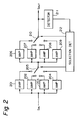
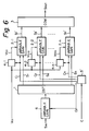
- Fig. 2 which illustrates a second previously proposed variable output amplifier apparatus (see: JP-A-60-212013)
- four amplifiers 201 through 204 are connected in parallel for receiving an input signal S IN .
- the amplifiers 201 through 204 are connected via a changeover switch 205 to four amplifiers 206 through 209 connected in parallel, the outputs of the amplifiers 206 to 209 being connected via a changeover switch 210 to a detector 211.
- the changeover switch 210 provides an output signal S OUT.
- the output signal of the detector 211 is supplied to a selection determination circuit 212 for controlling the changeover switches 205 and 210. That is, the selection determination circuit 212 selects an optimum combination of one of the amplifiers 201 through 204 and one of the amplifiers 206 through 209, in accordance with the output of the detector 211.
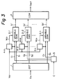
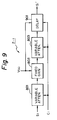
- a distributing unit 1 distributes an input signal S IN as signals S 1 , S 2 , .... S n to variable gain units 2-1, 2-2, ..., 2-n, respectively.
- Output signals S 1 ', S 2 ', ..., S n ' of the variable gain units 2-1, 2-2, ..., 2-n are combined by a combining unit 3 to generate an output signal S OUT .
- Power supply voltages V CC1 , V CC2 , ..., V CCn are applied to the variable gain units 2-1, 2-2, ..., 2-n from power supply control units 4-1, 4-2, ..., 4-n, respectively, which commonly receive a power supply V CC .
- variable gain units 2-1, 2-2, ..., 2-n and the power supply control units 4-1, 4-2, ..., 4-n are controlled by control signals C 1 , C 2 , ..., C n , respectively, of a control unit 5 which receives a gain control signal C.
- control signal C 1 rises from low to high
- the power supply control unit 4-1 promptly raises the power supply V CC1 from GND to V CC , and then, the gain of the variable gain unit 2-1 gradually starts to change from the minimum value to the maximum value.
- the gain of the variable gain unit 2-1 starts gradually to change from the minimum value to the maximum value, and then the power supply control unit 4-1 switches the power supply V CC1 from V CC to GND.
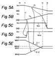
- Examples of the gains of the variable gain units 2-1, 2-2,..., 2-n are as shown in Fig. 4. That is, the gain of the variable gain unit 2-1 ranges from MAX1 to MIN1; the gain of the variable gain unit 2-2 ranges from MAX2 to MIN2: ...; and the gain of the variable gain unit 2-n ranges from MAXn to MINn.
- the value MIN1 is smaller than the value MAX2
- the value MIN2 is smaller than value MAX3, and so on.
- the control signals C 1 and C 2 are V CC and GND, respectively, as shown in Figs. 5A and 5B, and accordingly, the power supplies V CC1 and V CC2 are V CC and GND, respectively, as shown in Figs. 5C and 5D.
- the gain of,the variable gain unit 2-1 is MAX1
- the gain of the variable gain unit 2-2 is MIN2, as shown in Fig. 5E.
- the control signal C 1 starts to fall from V CC to GND, and almost simultaneously, at time t 1 , the control signal C 2 starts to rise from GND to V CC .
- the power supply V CC2 is switched by the power supply control unit 4-2 from GND to V CC .
- noise may be generated due to the rising of the power supply V CC2 in the variable gain unit 2-2.
- such noise can be neglected since the gain of the variable gain unit 2-2 is still MIN2.
- the gain of the variable gain unit 2-1 gradually decreases, as a result of the falling of the control signal C 1 , and the gain of the variable gain unit 2-2 gradually increases.
- the gain of the variable gain unit 2-1 reaches MIN1, while the gain of the variable gain unit 2-2 reaches MAX2.
- the power supply V CC1 is switched by the power supply control unit 4-1 from V CC to GND.
- noise may be generated due to the falling of the power supply V CC1 in the variable gain unit 2-1.
- noise can be neglected since the gain of the variable gain unit 2-1 is already MIN1.
- variable gain unit 2-1, 2-2, ..., 2-n the larger the power dissipation. Therefore, one of the variable gain units 2-1, 2-2, ..., 2-n, whose power dissipation is optimised at its maximum output power, and which can use the power supply effectively is selected.
- variable output amplifier apparatus of Fig. 3 if only one of the variable gain units 2-1, 2-2, 2-n is selected, the gain of the apparatus of Fig. 3 can be changed discretely from MAX1, MAX2 MAXn, as shown in Fig. 3. Therefore, if the number of the variable gain units 2-1, 2-2, ..., 2-n is increased, the gain of the apparatus of Fig. 3 can be almost continuously changed from MAX1 to MAXn.
- a variable gain unit 6 is added in a pre-stage to the elements of Fig. 3, thus obtaining a completely continuous change of the gain of the apparatus.
- the variable gain unit 6 is controlled by a control signal C 0 that is generated by a control unit 5'.
- the range of gain of the variable gain unit 5 is small, for example, form 0 to MAX, where MAX is larger than MAX2 in Fig. 4.
- control unit 5' An example of the operation of the control unit 5' is explained with reference to Figs. 7A, 7B, 7C and 7D.
- the gain control signal C gradually decreases so that the variable gain units 2-1, 2-2, ..., 2-n are sequentially activated as shown in Figs. 7A, 7B and 7C.
- the level of the gain control signal C 0 for the variable gain unit 6 decreases gradually and stepwise as the gain control signal C gradually decreases. Therefore, the control unit 5' can be formed by a voltage divider, or the like, in addition to the elements of the control unit 5 of Fig. 3.
- the variable attenuation units 801 and 803 are controlled by the control signal C i
- the fixed gain unit 802 and the delay unit 804 are activated by the power supply V CCi .
- the maximum attenuations of the variable attenuation units 801 and 803 are larger than the maximum gain of the fixed gain unit 802.
- the delay time of the delay unit 804 compensates for the fluctuation of the variable attenuation units 801 and 803, so that the delay times of the variable gain units 2-1, 2-2, ..., 2-n are equalized.
- variable attenuation units 801 and 803, defining the gain of the variable gain unit 2-i are gradually changed in response to the change of the control signal C i .
- the gain of the variable gain unit 2-i is gradually changed, as shown in Fig. 5E.
- the fixed gain unit 802 is turned ON and OFF when the attenuations of the variable attenuation units 801 and 803 are maximum. Therefore, the input/output impedance of the fixed gain unit 802 fluctuates, and there is no adverse effect on the input signal S i and the output signal S i '.
- a delay unit 901 is provided instead of the delay unit 804 of Fig. 8. That is, the delay unit 901 is also controlled by the control signal C i , so that the delay time of the entire variable gain unit 2-i is almost constant regardless of the change of the gain thereof.
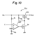
- a comparator CMP compares the voltage of the signal C with a reference voltage V R defined by resistors R 1 and R 2 , so as to control an N-channel MOS transistor Q n .
- a P-channel MOS transistor Q p is interposed between an input for the power supply V CC and an output for the power supply V CCi , and is controlled by the N-channel MOS transistor Q n .
- a resistor R 3 is connected between the gate of the P-channel MOS transistor Q p and the input for the power supply V CC .
- the comparator CMP turns OFF the n-channel MOS transistor Q n .
- the P-channel MOS transistor Q p is turned OFF.
- the power supply v CCi becomes GND (see Figs. 5A and 5C).
Landscapes
- Amplifiers (AREA)
- Control Of Amplification And Gain Control (AREA)
Applications Claiming Priority (2)
| Application Number | Priority Date | Filing Date | Title |
|---|---|---|---|
| JP7219232A JP3039613B2 (ja) | 1995-08-28 | 1995-08-28 | 増幅器 |
| JP219232/95 | 1995-08-28 |
Publications (2)
| Publication Number | Publication Date |
|---|---|
| EP0762637A2 true EP0762637A2 (fr) | 1997-03-12 |
| EP0762637A3 EP0762637A3 (fr) | 1998-01-28 |
Family
ID=16732280
Family Applications (1)
| Application Number | Title | Priority Date | Filing Date |
|---|---|---|---|
| EP96306236A Ceased EP0762637A3 (fr) | 1995-08-28 | 1996-08-28 | Amplificateur à puissance de sortie variable |
Country Status (7)
| Country | Link |
|---|---|
| US (1) | US5796306A (fr) |
| EP (1) | EP0762637A3 (fr) |
| JP (1) | JP3039613B2 (fr) |
| KR (1) | KR100191101B1 (fr) |
| CN (1) | CN1138339C (fr) |
| CA (1) | CA2184225C (fr) |
| TW (1) | TW393828B (fr) |
Cited By (7)
| Publication number | Priority date | Publication date | Assignee | Title |
|---|---|---|---|---|
| WO1999018678A1 (fr) * | 1997-10-06 | 1999-04-15 | Hughes Electronics Corporation | Systeme permettant une meilleure utilisation de l'energie de charge utile d'un satellite et technique afferente |
| US8149761B2 (en) | 2006-08-29 | 2012-04-03 | Wildblue Communications, Inc. | Incrementally increasing deployment of gateways |
| US8411798B2 (en) | 2008-11-05 | 2013-04-02 | Viasat, Inc. | Reducing receiver power dissipation |
| US8493881B2 (en) | 2009-09-04 | 2013-07-23 | Viasat, Inc. | Distributed cache—adaptive multicast architecture for bandwidth reduction |
| US8538328B2 (en) | 2008-09-11 | 2013-09-17 | Viasat, Inc. | Antenna and satellite alignment using beam projections |
| US8660142B2 (en) | 2008-09-25 | 2014-02-25 | Viasat, Inc. | Scheduling virtual bandwidth requests |
| US8730086B2 (en) | 2008-08-26 | 2014-05-20 | Viasat, Inc. | Weather detection using satellite communication signals |
Families Citing this family (18)
| Publication number | Priority date | Publication date | Assignee | Title |
|---|---|---|---|---|
| US6066983A (en) * | 1998-12-21 | 2000-05-23 | At&T Corp | PCS multi-carrier linear power amplifier |
| US6816016B2 (en) * | 2000-08-10 | 2004-11-09 | Tropian, Inc. | High-efficiency modulating RF amplifier |
| KR100837048B1 (ko) * | 2000-10-10 | 2008-06-11 | 엔엑스피 비 브이 | 증폭 회로 및 무선전기 신호 수신 디바이스 |
| KR100489693B1 (ko) * | 2001-02-16 | 2005-05-17 | 인티그런트 테크놀로지즈(주) | 선형성이 향상된 증폭 회로 및 믹서 회로 |
| JP2003258653A (ja) * | 2002-02-26 | 2003-09-12 | Toshiba Corp | 移動無線端末 |
| US7225967B2 (en) * | 2003-12-16 | 2007-06-05 | The Boeing Company | Structural assemblies and preforms therefor formed by linear friction welding |
| US7398911B2 (en) * | 2003-12-16 | 2008-07-15 | The Boeing Company | Structural assemblies and preforms therefor formed by friction welding |
| DE102004010169B4 (de) * | 2004-03-02 | 2010-09-02 | Infineon Technologies Ag | Schaltungsanordnung und Verfahren zur Reduzierung von Übersprechen sowie Verwendung derartiger Schaltungsanordnungen |
| US7492222B2 (en) * | 2006-06-30 | 2009-02-17 | Intel Corporation | Compound automatic gain control |
| US8731410B2 (en) * | 2007-10-02 | 2014-05-20 | Luxtera, Inc. | Method and system for split voltage domain receiver circuits |
| US10425165B1 (en) * | 2008-09-11 | 2019-09-24 | Luxtera, Inc. | Method and system for a distributed optical transmitter with local domain splitting |
| CN102043084B (zh) * | 2010-12-06 | 2014-10-15 | 上海思盛信息科技事务所 | 一种检测避雷器阻性电流的检测方法 |
| US8461928B2 (en) * | 2011-01-25 | 2013-06-11 | Provigent Ltd. | Constant-gain power amplifier |
| US8451062B2 (en) * | 2011-07-25 | 2013-05-28 | Honeywell International Inc. | Radiation hardened differential amplifier |
| JP6122583B2 (ja) * | 2012-06-05 | 2017-04-26 | ホーチキ株式会社 | 信号処理装置 |
| CN104682905B (zh) * | 2014-12-26 | 2017-08-11 | 北京航天测控技术有限公司 | 一种超宽带可变增益放大装置 |
| JP2016158176A (ja) * | 2015-02-25 | 2016-09-01 | 株式会社豊田中央研究所 | 電磁場変動センサ及び相互認識システム |
| EP3926827A1 (fr) * | 2020-06-18 | 2021-12-22 | Renesas Electronics America Inc. | Système d'amplificateur de gain variable, en particulier pour des systèmes de récepteur optique |
Family Cites Families (8)
| Publication number | Priority date | Publication date | Assignee | Title |
|---|---|---|---|---|
| JPS5883437A (ja) * | 1981-11-13 | 1983-05-19 | Hitachi Denshi Ltd | 送信電力制御方式 |
| JPS60212013A (ja) * | 1984-04-05 | 1985-10-24 | Nec Corp | 多段増幅器 |
| US4598252A (en) * | 1984-07-06 | 1986-07-01 | Itt Corporation | Variable gain power amplifier |
| US4636741A (en) * | 1985-11-01 | 1987-01-13 | Motorola, Inc. | Multi-level power amplifying circuitry for portable radio transceivers |
| JPH03104408A (ja) * | 1989-09-19 | 1991-05-01 | Fujitsu Ltd | 電力増幅器 |
| JPH0454006A (ja) * | 1990-06-22 | 1992-02-21 | Fujitsu Ltd | 増幅装置 |
| US5101173A (en) * | 1990-11-28 | 1992-03-31 | The United States Of America As Represented By The Secretary Of The Air Force | Stored program controlled module amplifier bias and amplitude/phase compensation apparatus |
| US5561395A (en) * | 1995-01-27 | 1996-10-01 | Motorola, Inc. | Method and apparatus for self-adjusting a multistage radio frequency power amplifier |
-
1995
- 1995-08-28 JP JP7219232A patent/JP3039613B2/ja not_active Expired - Fee Related
-
1996
- 1996-08-26 TW TW085110361A patent/TW393828B/zh not_active IP Right Cessation
- 1996-08-27 CA CA002184225A patent/CA2184225C/fr not_active Expired - Fee Related
- 1996-08-27 US US08/703,775 patent/US5796306A/en not_active Expired - Lifetime
- 1996-08-28 KR KR1019960037777A patent/KR100191101B1/ko not_active Expired - Fee Related
- 1996-08-28 CN CNB961133945A patent/CN1138339C/zh not_active Expired - Fee Related
- 1996-08-28 EP EP96306236A patent/EP0762637A3/fr not_active Ceased
Cited By (12)
| Publication number | Priority date | Publication date | Assignee | Title |
|---|---|---|---|---|
| WO1999018678A1 (fr) * | 1997-10-06 | 1999-04-15 | Hughes Electronics Corporation | Systeme permettant une meilleure utilisation de l'energie de charge utile d'un satellite et technique afferente |
| US6157812A (en) * | 1997-10-06 | 2000-12-05 | Hughes Electronics Corporation | System and method for enhanced satellite payload power utilization |
| US8149761B2 (en) | 2006-08-29 | 2012-04-03 | Wildblue Communications, Inc. | Incrementally increasing deployment of gateways |
| US8634768B2 (en) | 2006-08-29 | 2014-01-21 | Viasat, Inc. | Redundant communication path for satellite communication data |
| US8711758B2 (en) | 2006-08-29 | 2014-04-29 | Viasat, Inc. | Incrementally increasing deployment of gateways |
| US8730086B2 (en) | 2008-08-26 | 2014-05-20 | Viasat, Inc. | Weather detection using satellite communication signals |
| US9091763B2 (en) | 2008-08-26 | 2015-07-28 | Viasat, Inc. | Weather detection using satellite communication signals |
| US8538328B2 (en) | 2008-09-11 | 2013-09-17 | Viasat, Inc. | Antenna and satellite alignment using beam projections |
| US8660142B2 (en) | 2008-09-25 | 2014-02-25 | Viasat, Inc. | Scheduling virtual bandwidth requests |
| US8411798B2 (en) | 2008-11-05 | 2013-04-02 | Viasat, Inc. | Reducing receiver power dissipation |
| US8493881B2 (en) | 2009-09-04 | 2013-07-23 | Viasat, Inc. | Distributed cache—adaptive multicast architecture for bandwidth reduction |
| US9130889B2 (en) | 2009-09-04 | 2015-09-08 | Viasat, Inc. | Distributed cache—adaptive multicast architecture for bandwidth reduction |
Also Published As
| Publication number | Publication date |
|---|---|
| CN1138339C (zh) | 2004-02-11 |
| US5796306A (en) | 1998-08-18 |
| KR100191101B1 (ko) | 1999-06-15 |
| CN1155782A (zh) | 1997-07-30 |
| EP0762637A3 (fr) | 1998-01-28 |
| KR970013658A (ko) | 1997-03-29 |
| CA2184225C (fr) | 1999-08-17 |
| TW393828B (en) | 2000-06-11 |
| JP3039613B2 (ja) | 2000-05-08 |
| CA2184225A1 (fr) | 1997-03-01 |
| JPH0964667A (ja) | 1997-03-07 |
Similar Documents
| Publication | Publication Date | Title |
|---|---|---|
| EP0762637A2 (fr) | Amplificateur à puissance de sortie variable | |
| US5831477A (en) | Power amplifier system with variable output | |
| US6215987B1 (en) | Mobile communication transmitter capable of selectively activating amplifiers | |
| KR100423854B1 (ko) | 고주파증폭기,송신장치및수신장치 | |
| US6157253A (en) | High efficiency power amplifier circuit with wide dynamic backoff range | |
| US5126686A (en) | RF amplifier system having multiple selectable power output levels | |
| US7170341B2 (en) | Low power consumption adaptive power amplifier | |
| US6337974B1 (en) | Cellular mobile telephone terminal | |
| JP2003204230A (ja) | 信号を増幅するための方法および装置 | |
| KR19990076806A (ko) | 효율적인 병렬단 전력 증폭기 | |
| US6624700B2 (en) | Radio frequency power amplifier for cellular telephones | |
| US7454182B2 (en) | Attenuator with switch function and mobile telephone terminal device using the same | |
| KR20010075166A (ko) | 전력 증폭기의 포화 상태를 방지하기 위한 방법 및 장치 | |
| US12362715B2 (en) | Voltage controlled attenuator | |
| US5160898A (en) | Power amplifier | |
| KR100251560B1 (ko) | 부호분할 다중 접속방식 단말기의 외부 간섭신호 제거장치 | |
| US5239695A (en) | Radio-frequency power control circuit of mobile radiophone | |
| US7023278B1 (en) | Digital power amplifier level control | |
| US7245170B2 (en) | Attenuator and portable telephone terminal apparatus using the same | |
| US6253070B1 (en) | Diode amplifier bypass circuit | |
| CA2371593A1 (fr) | Circuit amplificateur | |
| GB2316561A (en) | Improving the efficiency of a power amplifier by selecting stored values of supply and/or bias voltage in dependence on measured output power | |
| KR100303309B1 (ko) | 이동통신단말기에서전류제어를통한증폭기의선형성개선장치 | |
| JPH09148945A (ja) | 送信出力制御方式 | |
| JPH09199960A (ja) | 電力増幅器 |
Legal Events
| Date | Code | Title | Description |
|---|---|---|---|
| PUAI | Public reference made under article 153(3) epc to a published international application that has entered the european phase |
Free format text: ORIGINAL CODE: 0009012 |
|
| AK | Designated contracting states |
Kind code of ref document: A2 Designated state(s): GB SE |
|
| PUAL | Search report despatched |
Free format text: ORIGINAL CODE: 0009013 |
|
| AK | Designated contracting states |
Kind code of ref document: A3 Designated state(s): GB SE |
|
| 17P | Request for examination filed |
Effective date: 19980122 |
|
| 17Q | First examination report despatched |
Effective date: 20020723 |
|
| STAA | Information on the status of an ep patent application or granted ep patent |
Free format text: STATUS: THE APPLICATION HAS BEEN REFUSED |
|
| 18R | Application refused |
Effective date: 20040129 |