EP0759643A1 - Mikrowellenfilter - Google Patents
Mikrowellenfilter Download PDFInfo
- Publication number
- EP0759643A1 EP0759643A1 EP96306059A EP96306059A EP0759643A1 EP 0759643 A1 EP0759643 A1 EP 0759643A1 EP 96306059 A EP96306059 A EP 96306059A EP 96306059 A EP96306059 A EP 96306059A EP 0759643 A1 EP0759643 A1 EP 0759643A1
- Authority
- EP
- European Patent Office
- Prior art keywords
- filter
- regulating element
- switch
- radio frequency
- frequency filter
- Prior art date
- Legal status (The legal status is an assumption and is not a legal conclusion. Google has not performed a legal analysis and makes no representation as to the accuracy of the status listed.)
- Withdrawn
Links
Images


Classifications
-
- H—ELECTRICITY
- H01—ELECTRIC ELEMENTS
- H01P—WAVEGUIDES; RESONATORS, LINES, OR OTHER DEVICES OF THE WAVEGUIDE TYPE
- H01P1/00—Auxiliary devices
- H01P1/20—Frequency-selective devices, e.g. filters
- H01P1/201—Filters for transverse electromagnetic waves
- H01P1/205—Comb or interdigital filters; Cascaded coaxial cavities
- H01P1/2056—Comb filters or interdigital filters with metallised resonator holes in a dielectric block
Definitions
- the present invention relates to a radio frequency filter comprising a first transmission line resonator and a second transmission line resonator.
- Radio devices generally employ filters which are based on transmission line resonators with electromagnetic couplings between them. Between transmission line resonators coupled through an insulating material by means of electromagnetic fields there usually is both a capacitive and an inductive coupling, which together result in a certain frequency response in the filter constituted by the resonators.
- the capacitive and inductive couplings together cause in the frequency response of a bandpass filter a so-called transmission zero, or a certain relatively narrow frequency area which limits the pass band of the filter on one side and in which the attenuation of the filter is particularly high.
- ⁇ /4 resonators ie.
- the location of said transmission zero with respect to the pass band of the filter depends on the interrelation of the strengths of the capacitive and inductive couplings between the resonators. If the capacitive coupling is dominant, the transmission zero is located below the pass band, and if the inductive coupling is dominant, the transmission zero is located above the pass band.
- the strength of the coupling between two resonators depends on the combined effect of the capacitive and inductive coupling between them.
- the phase difference between the capacitive and inductive coupling is 180 degrees, which means they have opposite signs and therefore tend to cancel each other. Because of this, both couplings in a bandpass filter can be made high enough for the zero of the frequency response to be located at a suitable distance from the pass band while the combined effect is small enough to realize the bandpass characteristic of the filter. If the absolute values of the inductive and capacitive couplings are identical, the total coupling between the resonators is zero, in which case they cannot be used to realize a bandpass filter.
- a radio frequency filter comprising a first transmission line resonator and a second transmission line resonator and an electromagnetic coupling between the first and second transmission line resonators, which coupling comprises a capacitive and inductive portion, characterized in that the radio frequency filter includes means for changing the capacitive and/or inductive portion of said coupling to affect the frequency response of the radio frequency filter, said means comprising an electrically conductive element and means for changing the potential of the conductive element.
- the potential of the conductive element is changed on the basis of a signal, ideally an electric signal.
- Exemplary embodiments in accordance with the invention may provide a radio frequency filter based on transmission line resonators the frequency response of which can be changed electrically. Also exemplary embodiments in accordance with the invention may provide a bandpass filter operating at radio frequencies in which the location on the frequency axis of the frequency response zero limiting the pass band can be altered electrically. Furthermore exemplary embodiments in accordance with the invention may provide a filter as described above in which the frequency response adjustment is realized in a simple manner.
- Embodiments in accordance with the invention may be achieved by adding an electrically controllable switch or an electrically adjustable reactive component between a prior-art passive regulating element located in the vicinity of the resonators and the ground potential of the filter to change the reactance between said regulating element and the filter ground plane.
- Embodiments in accordance with the invention may relate to the adjustment of the frequency response of a filter, based on transmission line resonators and operating at radio frequencies.
- the adjustment may be directed especially to the location on the frequency axis of the so-called transmission zero, or the attenuation peak limiting the pass band of a bandpass filter.
- the frequency response of the filter particularly the location of the transmission zero, or the frequency response zero, could be altered using an external control voltage or current.
- Embodiments in accordance with the invention may be based on the idea that when examining a prior-art passive regulating element located in the vicinity of resonators, we can see that its regulating characteristics are affected, in addition to its location and conductivity properties, by its potential which can be electrically altered using the method in accordance with the invention.
- an electrically controlled switch advantageously a PIN diode, field-effect transistor or other voltage- and/or current-controlled semiconductor switch known to one skilled in the art or an electrically variable reactive element, advantageously a capacitance diode, or a varactor, may be placed between said regulating element, which can be e.g. a metal strip, and the ground potential.
- a semiconductor switch made of gallium arsenide (GaAs) is fast and reliable, whereby the frequency response of a filter can be changed very quickly between two different states. Adding more regulating elements and more switches one can implement adjustment arrangements with more steps. By placing a variable reactive component, such as a capacitance diode, between the regulating element and the ground potential of the filter instead of a switch, one can have an arrangement in which the frequency response of the filter can be steplessly adjusted by means of a control voltage and/or current.
- GaAs gallium arsenide
- Fig. 1a there is a coupling K between two transmission line resonators R1, R2, which can be influenced with a control signal C.
- the practical implementation of Fig. 1a can be realized in many ways by embodiments in accordance with the present invention.
- Fig. 1b shows a circuit diagram of an advantageous embodiment wherein an electrically conducting regulating element S3, which affects the coupling between resonators R1 and R2, can be grounded by means of switch SW1 when desired.
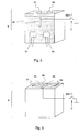
- Fig. 2 shows a dielectric filter made of one piece (so-called monoblock) comprising two transmission line resonators R1, R2.
- the manufacture of this kind of filter will not be described since it is known to one skilled in the art.
- the dielectric block B which constitutes the body of the filter is advantageously of ceramic material, and the resonators R1 and R2 are cylindrical holes in the block, extending from the lower surface of the block to the upper surface (the top surface in the figure) of the block, and the walls of the holes are coated with a conductive material. Most of the side surfaces of the block B are also coated with a conductive material, which is indicated by white colour in the figure.
- Fig. 2 is not entirely coated, but strip-like conductive patterns S1, S2 and S3 are formed on it.
- the top side shown in Fig. 2 is uncoated.
- the uncoated ceramic material is shown as gray in the figure.
- the two widest conductive patterns S1 and S2 constitute the input and output port of the filter, ie. they provide the coupling interface to the resonators R1 and R2.
- the third conductive pattern S3 is a regulating element known in the prior art which, as such, strengthens in a known manner the capacitive coupling between the resonators R1 and R2.
- the alternative embodiment shown in Fig. 3 is also a dielectric filter which differs from the embodiment in Fig. 2 in that there the front side is coated with a conductive material and the conductive patterns S1, S2 and S3 are formed on the top surface which is uncoated except for the conductive patterns.
- the embodiments shown in Figs. 1b, 2 and 3 include a switch SW1, which is shown in the figures only diagrammatically, but which is realized by a PIN diode, field-effect transistor or other semiconductor switch in a manner which is known to one skilled in the art.
- the switch component is coupled e.g. by soldering to connection pads (not shown in the figures) which are formed on the surface of the dielectric block B in the same way as the other conductive patterns S1, S2 and S3.
- a control signal C which opens and closes the switch SW1, is coupled to said switch component by means of strip lines (not shown) formed on the surface of the dielectric.
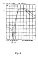
- Fig. 4 shows a qualitative representation of a real frequency response measurement, in which the frequency response of a filter according to the embodiment shown in Fig.
- Fig. 4 shows clearly that closing the switch SW1, ie. grounding the regulating element S3, shifts the transmission zero in the frequency response upwards on the frequency axis, or, in Fig. 4, to the right, from position O1 to position O1'.
- the pass band of the filter, or the frequency area with the lowest attenuation becomes somewhat narrower when the switch SW1 is closed, because the absolute value of the combined effect of the capacitive and inductive coupling becomes smaller.
- Fig. 5 is a simplified illustration of a frequency response measurement for the frequency response of a third embodiment of the invention. Since the transmission zero is in this case above the pass band, ie. on the right-hand side in the figure, the inductive coupling is dominant in a filter according to the third embodiment. It is clear to one skilled in the art how to implement a filter the frequency response of which qualitatively corresponds to the solid-line curve using known methods discussed above in conjunction with the description of the prior art, advantageously a regulating element made of a conductive material. When such a regulating element is grounded according to the invention, the relative portion of the inductive coupling increases compared to the capacitive coupling, whereby the transmission zero is shifted upwards on the frequency axis, ie. in Fig. 5, to the right, from position 02 to position 02'. At the same time the pass band of the filter becomes somewhat wider, because the absolute value of the combined effect of the capacitive and inductive coupling becomes greater.
- This fourth embodiment of the invention is shown as a circuit diagram in Fig. 6a including regulating elements S3 and S4, which advantageously are strip lines, and corresponding switches SW1 and SW2.
- the regulating element S3 primarily affects the capacitive coupling between the resonators R1 and R2
- the regulating element S4 primarily affects the inductive coupling between the resonators R1 and R2.
- the switches are controlled by separate control signals C and C'.
- a further alternative is to use, instead of the aforementioned simple two-state switch SW1, a switch SW3 with three or more states which is included in the fifth embodiment of the invention as shown in the circuit diagram of Fig. 6b.
- a switch SW3 with three or more states which is included in the fifth embodiment of the invention as shown in the circuit diagram of Fig. 6b.
- the switch SW3 could be open in its first state, connect the regulating element S3 directly to the ground in the second state and, in the third state, ground the regulating element S3 through a transmission line SL1 which advantageously could be a strip line similar to the other strip lines in the filter structure. Grounding through a transmission line SL1 would affect the resonance characteristics of the regulating element S3 differently than direct grounding, whereby the effect on the frequency response would be different.
- Various other embodiments may be realised within the scope of the inventive idea disclosed here.
- a coupling is implemented by replacing the switch SW1 mentioned above with a reactive component, advantageously a capacitance diode, or varactor D controlled with a voltage and/or current signal, as shown in the circuit diagram of Fig. 7 illustrating a sixth embodiment of the invention.
- the reactance of the capacitance diode can be steplessly adjusted by changing the voltage serving as control signal C"'.
- Fig. 8 is a simplified representation of a frequency response measurement in which the frequency response of a filter according to the embodiment shown in Fig. 7 is measured with three different values of the control voltage C"'. Each curve represents a certain value of the control voltage C"'.
- a bandpass filter in accordance with the invention the shifting of the transmission zero is easy and quick, and only one switch and a suitable ground strip line need be added to a filter according to the prior art.
- the invention is in no way limited to bandpass filters only but it can be generalized to apply to other transmission line resonators when their frequency response characteristics need be electrically changed. Neither is the invention limited to dielectric filters, but it can be applied in all filter structures which are based on transmission line resonators and in which the coupling between the resonators can be affected with a conductive regulating element.
- Another example of a possible filter structure is a helix filter based on cylindrical coil conductors, known e.g. from Finnish Patent Fl-90157, wherein the regulating elements according to the invention can be manufactured as strip lines in the same way as in the embodiments described above. Filters according to the invention can be advantageously used in small radio communication devices, such as mobile phones.
Landscapes
- Physics & Mathematics (AREA)
- Electromagnetism (AREA)
- Control Of Motors That Do Not Use Commutators (AREA)
Applications Claiming Priority (2)
| Application Number | Priority Date | Filing Date | Title |
|---|---|---|---|
| FI953962 | 1995-08-23 | ||
| FI953962A FI953962A (fi) | 1995-08-23 | 1995-08-23 | Esto-ominaisuuksiltaan säädettävä kaistanpäästosuodatin |
Publications (1)
| Publication Number | Publication Date |
|---|---|
| EP0759643A1 true EP0759643A1 (de) | 1997-02-26 |
Family
ID=8543900
Family Applications (1)
| Application Number | Title | Priority Date | Filing Date |
|---|---|---|---|
| EP96306059A Withdrawn EP0759643A1 (de) | 1995-08-23 | 1996-08-20 | Mikrowellenfilter |
Country Status (4)
| Country | Link |
|---|---|
| EP (1) | EP0759643A1 (de) |
| AU (1) | AU5944796A (de) |
| CA (1) | CA2179673A1 (de) |
| FI (1) | FI953962A (de) |
Cited By (1)
| Publication number | Priority date | Publication date | Assignee | Title |
|---|---|---|---|---|
| DE19857358A1 (de) * | 1998-11-03 | 2000-05-18 | Samsung Electro Mech | Dielektrisches Filter |
Citations (3)
| Publication number | Priority date | Publication date | Assignee | Title |
|---|---|---|---|---|
| US5055808A (en) * | 1990-09-21 | 1991-10-08 | Motorola, Inc. | Bandwidth agile, dielectrically loaded resonator filter |
| EP0481607A1 (de) * | 1990-10-15 | 1992-04-22 | Hewlett-Packard Company | Amplitudenkorrektor von von feldgekoppelten Varaktoren abgestimmten Filtern |
| EP0520641A1 (de) * | 1991-06-25 | 1992-12-30 | Lk-Products Oy | Abstimmbare Resonatoranordnung |
-
1995
- 1995-08-23 FI FI953962A patent/FI953962A/fi unknown
-
1996
- 1996-06-21 CA CA 2179673 patent/CA2179673A1/en not_active Abandoned
- 1996-07-11 AU AU59447/96A patent/AU5944796A/en not_active Abandoned
- 1996-08-20 EP EP96306059A patent/EP0759643A1/de not_active Withdrawn
Patent Citations (3)
| Publication number | Priority date | Publication date | Assignee | Title |
|---|---|---|---|---|
| US5055808A (en) * | 1990-09-21 | 1991-10-08 | Motorola, Inc. | Bandwidth agile, dielectrically loaded resonator filter |
| EP0481607A1 (de) * | 1990-10-15 | 1992-04-22 | Hewlett-Packard Company | Amplitudenkorrektor von von feldgekoppelten Varaktoren abgestimmten Filtern |
| EP0520641A1 (de) * | 1991-06-25 | 1992-12-30 | Lk-Products Oy | Abstimmbare Resonatoranordnung |
Cited By (2)
| Publication number | Priority date | Publication date | Assignee | Title |
|---|---|---|---|---|
| DE19857358A1 (de) * | 1998-11-03 | 2000-05-18 | Samsung Electro Mech | Dielektrisches Filter |
| US6169464B1 (en) | 1998-11-03 | 2001-01-02 | Samsung Electro-Mechanics Co., Ltd. | Dielectric filter |
Also Published As
| Publication number | Publication date |
|---|---|
| FI953962A (fi) | 1997-02-24 |
| CA2179673A1 (en) | 1997-02-24 |
| AU5944796A (en) | 1997-02-27 |
| FI953962A0 (fi) | 1995-08-23 |
Similar Documents
| Publication | Publication Date | Title |
|---|---|---|
| US5815048A (en) | Switchable duplex filter | |
| US6037848A (en) | Electrically regulated filter having a selectable stop band | |
| US5793269A (en) | Stepwise regulated filter having a multiple-step switch | |
| FI88442C (fi) | Foerfarande foer foerskjutning av den karakteristika kurvan av en resonator i frekvensplanet och en resonatorkonstruktion | |
| FI95851B (fi) | Siirtojohtoresonaattorin sähköinen taajuudensäätökytkentä sekä säädettävä suodatin | |
| US5065120A (en) | Frequency agile, dielectrically loaded resonator filter | |
| US20030128084A1 (en) | Compact bandpass filter for double conversion tuner | |
| US6522220B2 (en) | Frequency variable filter, antenna duplexer, and communication apparatus incorporating the same | |
| US6346853B1 (en) | Predistortion linearizer circuit | |
| Presser | Varactor-tunable, high-Q microwave filter | |
| US6288620B1 (en) | Antenna-duplexer and communication apparatus | |
| US6798319B2 (en) | High-frequency filter | |
| US4471330A (en) | Digital phase bit for microwave operation | |
| US5307032A (en) | Wideband frequency distributed signal selector using electromagnetic coupling | |
| RU2649050C1 (ru) | Микроволновый аналоговый фазовращатель и система, содержащая его | |
| FI97754C (fi) | Resonaattorin resonanssitaajuuden sähköinen säätö | |
| EP0759643A1 (de) | Mikrowellenfilter | |
| US7479856B2 (en) | High-frequency filter using coplanar line resonator | |
| JPH10247801A (ja) | Rfスイッチ回路および送受共用器 | |
| JPH08213802A (ja) | 高周波スイッチ回路 | |
| JP2846240B2 (ja) | 周波数帯域可変フィルタ | |
| JP4189971B2 (ja) | 周波数可変型高周波フィルタ | |
| KR100305577B1 (ko) | 유전체 듀플렉서의 제조방법 | |
| JPH0253306A (ja) | ミキサ回路 | |
| CA2020365A1 (en) | Filter |
Legal Events
| Date | Code | Title | Description |
|---|---|---|---|
| PUAI | Public reference made under article 153(3) epc to a published international application that has entered the european phase |
Free format text: ORIGINAL CODE: 0009012 |
|
| AK | Designated contracting states |
Kind code of ref document: A1 Designated state(s): CH DE DK FR GB IT LI SE |
|
| STAA | Information on the status of an ep patent application or granted ep patent |
Free format text: STATUS: THE APPLICATION IS DEEMED TO BE WITHDRAWN |
|
| 18D | Application deemed to be withdrawn |
Effective date: 19970827 |
|
| RAP1 | Party data changed (applicant data changed or rights of an application transferred) |
Owner name: LK-PRODUCTS OY |