EP0758788A1 - Solid electrolytic capacitor and its manufacturing method - Google Patents
Solid electrolytic capacitor and its manufacturing method Download PDFInfo
- Publication number
- EP0758788A1 EP0758788A1 EP96904299A EP96904299A EP0758788A1 EP 0758788 A1 EP0758788 A1 EP 0758788A1 EP 96904299 A EP96904299 A EP 96904299A EP 96904299 A EP96904299 A EP 96904299A EP 0758788 A1 EP0758788 A1 EP 0758788A1
- Authority
- EP
- European Patent Office
- Prior art keywords
- chip
- solid electrolytic
- substrate
- layer
- master substrate
- Prior art date
- Legal status (The legal status is an assumption and is not a legal conclusion. Google has not performed a legal analysis and makes no representation as to the accuracy of the status listed.)
- Granted
Links
- 239000003990 capacitor Substances 0.000 title claims abstract description 109
- 239000007787 solid Substances 0.000 title claims abstract description 72
- 238000004519 manufacturing process Methods 0.000 title description 11
- 239000000758 substrate Substances 0.000 claims abstract description 175
- 229910052751 metal Inorganic materials 0.000 claims abstract description 65
- 239000002184 metal Substances 0.000 claims abstract description 65
- 239000011248 coating agent Substances 0.000 claims abstract description 36
- 238000000576 coating method Methods 0.000 claims abstract description 36
- 239000007784 solid electrolyte Substances 0.000 claims abstract description 34
- 239000011347 resin Substances 0.000 claims abstract description 32
- 229920005989 resin Polymers 0.000 claims abstract description 32
- 239000000843 powder Substances 0.000 claims abstract description 26
- 238000000034 method Methods 0.000 claims abstract description 23
- 230000008569 process Effects 0.000 claims abstract description 17
- 238000010292 electrical insulation Methods 0.000 claims abstract description 4
- 238000005520 cutting process Methods 0.000 claims description 13
- 238000005245 sintering Methods 0.000 claims description 12
- 229910021332 silicide Inorganic materials 0.000 claims description 11
- FVBUAEGBCNSCDD-UHFFFAOYSA-N silicide(4-) Chemical compound [Si-4] FVBUAEGBCNSCDD-UHFFFAOYSA-N 0.000 claims description 11
- 229910010293 ceramic material Inorganic materials 0.000 claims description 9
- 238000010438 heat treatment Methods 0.000 claims description 7
- 229910052710 silicon Inorganic materials 0.000 claims description 7
- 239000010703 silicon Substances 0.000 claims description 7
- 239000011810 insulating material Substances 0.000 claims description 6
- 239000000126 substance Substances 0.000 claims description 6
- 239000000463 material Substances 0.000 claims description 5
- 239000007769 metal material Substances 0.000 claims 1
- GUVRBAGPIYLISA-UHFFFAOYSA-N tantalum atom Chemical compound [Ta] GUVRBAGPIYLISA-UHFFFAOYSA-N 0.000 description 67
- 239000010408 film Substances 0.000 description 58
- 229910052715 tantalum Inorganic materials 0.000 description 49
- 230000001965 increasing effect Effects 0.000 description 8
- 239000000243 solution Substances 0.000 description 8
- OKTJSMMVPCPJKN-UHFFFAOYSA-N Carbon Chemical compound [C] OKTJSMMVPCPJKN-UHFFFAOYSA-N 0.000 description 7
- 229910002804 graphite Inorganic materials 0.000 description 7
- 239000010439 graphite Substances 0.000 description 7
- MIVBAHRSNUNMPP-UHFFFAOYSA-N manganese(2+);dinitrate Chemical compound [Mn+2].[O-][N+]([O-])=O.[O-][N+]([O-])=O MIVBAHRSNUNMPP-UHFFFAOYSA-N 0.000 description 7
- 238000004544 sputter deposition Methods 0.000 description 7
- PXHVJJICTQNCMI-UHFFFAOYSA-N Nickel Chemical compound [Ni] PXHVJJICTQNCMI-UHFFFAOYSA-N 0.000 description 6
- 238000007493 shaping process Methods 0.000 description 6
- XUIMIQQOPSSXEZ-UHFFFAOYSA-N Silicon Chemical compound [Si] XUIMIQQOPSSXEZ-UHFFFAOYSA-N 0.000 description 5
- 239000007864 aqueous solution Substances 0.000 description 5
- BPUBBGLMJRNUCC-UHFFFAOYSA-N oxygen(2-);tantalum(5+) Chemical compound [O-2].[O-2].[O-2].[O-2].[O-2].[Ta+5].[Ta+5] BPUBBGLMJRNUCC-UHFFFAOYSA-N 0.000 description 5
- 238000000206 photolithography Methods 0.000 description 5
- PBCFLUZVCVVTBY-UHFFFAOYSA-N tantalum pentoxide Inorganic materials O=[Ta](=O)O[Ta](=O)=O PBCFLUZVCVVTBY-UHFFFAOYSA-N 0.000 description 5
- 239000010409 thin film Substances 0.000 description 5
- NBIIXXVUZAFLBC-UHFFFAOYSA-N Phosphoric acid Chemical compound OP(O)(O)=O NBIIXXVUZAFLBC-UHFFFAOYSA-N 0.000 description 4
- NUJOXMJBOLGQSY-UHFFFAOYSA-N manganese dioxide Chemical compound O=[Mn]=O NUJOXMJBOLGQSY-UHFFFAOYSA-N 0.000 description 4
- 230000004048 modification Effects 0.000 description 4
- 238000012986 modification Methods 0.000 description 4
- 230000003647 oxidation Effects 0.000 description 4
- 238000007254 oxidation reaction Methods 0.000 description 4
- 239000002245 particle Substances 0.000 description 4
- 229920002120 photoresistant polymer Polymers 0.000 description 4
- 229910000679 solder Inorganic materials 0.000 description 4
- 230000008901 benefit Effects 0.000 description 3
- 239000011230 binding agent Substances 0.000 description 3
- 230000007423 decrease Effects 0.000 description 3
- 229910052759 nickel Inorganic materials 0.000 description 3
- 229920003002 synthetic resin Polymers 0.000 description 3
- 239000000057 synthetic resin Substances 0.000 description 3
- 229910052582 BN Inorganic materials 0.000 description 2
- PZNSFCLAULLKQX-UHFFFAOYSA-N Boron nitride Chemical compound N#B PZNSFCLAULLKQX-UHFFFAOYSA-N 0.000 description 2
- 229910052581 Si3N4 Inorganic materials 0.000 description 2
- VYPSYNLAJGMNEJ-UHFFFAOYSA-N Silicium dioxide Chemical compound O=[Si]=O VYPSYNLAJGMNEJ-UHFFFAOYSA-N 0.000 description 2
- 229910000147 aluminium phosphate Inorganic materials 0.000 description 2
- 239000004020 conductor Substances 0.000 description 2
- 230000003247 decreasing effect Effects 0.000 description 2
- 238000005530 etching Methods 0.000 description 2
- 238000007654 immersion Methods 0.000 description 2
- 238000009413 insulation Methods 0.000 description 2
- 239000012466 permeate Substances 0.000 description 2
- 238000005268 plasma chemical vapour deposition Methods 0.000 description 2
- 238000006116 polymerization reaction Methods 0.000 description 2
- 239000000047 product Substances 0.000 description 2
- HBMJWWWQQXIZIP-UHFFFAOYSA-N silicon carbide Chemical compound [Si+]#[C-] HBMJWWWQQXIZIP-UHFFFAOYSA-N 0.000 description 2
- 229910010271 silicon carbide Inorganic materials 0.000 description 2
- HQVNEWCFYHHQES-UHFFFAOYSA-N silicon nitride Chemical compound N12[Si]34N5[Si]62N3[Si]51N64 HQVNEWCFYHHQES-UHFFFAOYSA-N 0.000 description 2
- 229910052814 silicon oxide Inorganic materials 0.000 description 2
- 239000013585 weight reducing agent Substances 0.000 description 2
- 238000005452 bending Methods 0.000 description 1
- 239000000919 ceramic Substances 0.000 description 1
- 238000009792 diffusion process Methods 0.000 description 1
- 230000002708 enhancing effect Effects 0.000 description 1
- 239000003822 epoxy resin Substances 0.000 description 1
- 238000012685 gas phase polymerization Methods 0.000 description 1
- 230000006872 improvement Effects 0.000 description 1
- 230000001678 irradiating effect Effects 0.000 description 1
- 229910044991 metal oxide Inorganic materials 0.000 description 1
- 150000004706 metal oxides Chemical class 0.000 description 1
- 239000002923 metal particle Substances 0.000 description 1
- 238000000465 moulding Methods 0.000 description 1
- 230000001590 oxidative effect Effects 0.000 description 1
- 229920000647 polyepoxide Polymers 0.000 description 1
- 229920001721 polyimide Polymers 0.000 description 1
- 239000009719 polyimide resin Substances 0.000 description 1
- 229920000642 polymer Polymers 0.000 description 1
- 230000009467 reduction Effects 0.000 description 1
- 229910052709 silver Inorganic materials 0.000 description 1
- 239000004332 silver Substances 0.000 description 1
- 238000005549 size reduction Methods 0.000 description 1
Images








Classifications
-
- H—ELECTRICITY
- H01—ELECTRIC ELEMENTS
- H01G—CAPACITORS; CAPACITORS, RECTIFIERS, DETECTORS, SWITCHING DEVICES, LIGHT-SENSITIVE OR TEMPERATURE-SENSITIVE DEVICES OF THE ELECTROLYTIC TYPE
- H01G9/00—Electrolytic capacitors, rectifiers, detectors, switching devices, light-sensitive or temperature-sensitive devices; Processes of their manufacture
- H01G9/004—Details
- H01G9/04—Electrodes or formation of dielectric layers thereon
-
- H—ELECTRICITY
- H01—ELECTRIC ELEMENTS
- H01G—CAPACITORS; CAPACITORS, RECTIFIERS, DETECTORS, SWITCHING DEVICES, LIGHT-SENSITIVE OR TEMPERATURE-SENSITIVE DEVICES OF THE ELECTROLYTIC TYPE
- H01G9/00—Electrolytic capacitors, rectifiers, detectors, switching devices, light-sensitive or temperature-sensitive devices; Processes of their manufacture
- H01G9/15—Solid electrolytic capacitors
Definitions
- This invention relates generally to solid electrolytic capacitors such as tantalum capacitors. More specifically, the present invention relates to a solid electrolytic capacitor which is suitably designed for surface mounting. The present invention also relates to a process for making such a solid electrolytic capacitor.
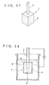
- metal powder such as tantalum powder is compacted into a porous chip 2 from which a metal anode wire 3 made of e.g. tantalum projects out and thereafter sintered.
- the chip 2 is immersed in a chemical solution A such as aqueous solution of phosphoric acid, and a direct current is passed between the anode wire 3 and the solution A for performing anodic oxidation.
- a dielectric film 4 of tantalum pentoxide for example is formed on the surfaces of the metal particles of the chip 2.
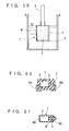
- the steps are repeated plural times which comprise immersing the chip 2 in an aqueous solution B of manganese nitrate until the manganese nitrate solution B permeates into the chip 2, and thereafter lifting out the chip for baking.
- a solid electrolyte layer 5 of a metal oxide such as manganese dioxide is formed on the surface of the dielectric film 4.
- a cathode film made of a metal such as silver or nickel is formed after graphitizing the surface of the solid electrolyte layer 5 of the chip 2. This provides a capacitor element 1.
- the anode wire 3 projecting from the chip 2 is indispensable and cannot be obviated. Therefore, it was conventional to employ the structure of Fig. 60 or 61 for making a surface-mounting type solid electrolytic capacitor by incorporating the capacitor element 1.
- the capacitor element 1 is arranged between a cathode lead terminal 6a and an anode lead terminal 6b.
- the chip 2 of the capacitor element 1 is attached to the cathode lead terminal 6b, whereas the anode wire 3 is attached to the anode lead terminal 6a.
- the capacitor element 1 together with the inner ends of the respective lead terminals 6a, 6b is enclosed in a molded synthetic resin package 7.
- the solid electrolytic capacitor of such a structure is disclosed in Japanese Patent Application Laid-open No. 60-220922 for example.
- the capacitor element 1 is enclosed in a molded synthetic resin package 8 in a manner such that the tip portion of the anode wire 3 and the end face of the chip 2 opposite to the anode wire 3 are exposed.
- the exposed tip portion of the anode wire 3 is formed with an anode terminal portion 9a made of e.g. solder, whereas the exposed end face of the chip is formed with a cathode terminal portion 9b made of e.g. solder.
- the capacitor element 1 need be enclosed in the resin package7, 8 in such a manner as to contain both the chip 2 and the projecting anode wire 3. Therefore, the package 7, 8 must be larger in size than the chip 2 of the capacitor element 1 by as much as the anode wire 3 projects out from the chip 2, so that the ratio of the volume of the chip 2 relative to the overall volume of the capacitor decreases to result in a volume efficiency reduction. Further, the effective volume of the chip 2 also reduces by as much as the anode wire 3 is embedded in the chip 2. Due to these factors, the prior art solid electrolytic capacitor poses difficulty in increasing the capacitance per unit volume while also giving rise to a weight increase problem. These problems are particularly remarkable with respect the solid electrolytic capacitor having the structure of Figs. 60 which incorporates the two lead terminals 6a, 6b.
- each of the projecting anode wires 3 of plural sintered chips 1 is attached to a metal bar 10 of e.g. tantalum, as shown in Fig. 62.
- various process steps are performed which include forming the dielectric layer 4 by immersion in the chemical solution A (Fig. 58), forming the solid electrolyte layer 5 by immersion in the aqueous solution B of manganese nitrate (Fig. 59), graphitizing, forming the cathode film, and the like.
- each of the capacitor elements 1 is cut off the metal bar 10. Therefore, there is a limitation in the number of capacitor elements 1 which can be produced by using the single metal bar 10, so that there is difficulty in meeting the requirements for mass production. Thus, combined with a low yield of production, a production cost will result.
- the solid electrolytic capacitor of the type shown in Fig. 60 incorporates the two lead terminals 6a, 6b, it is necessary to perform additional steps of attaching the respective lead terminals 6a, 6b to the capacitor element 1 and bending the lead terminals 6a, 6b as shown.
- the production cost becomes even higher in comparison with the solid electrolytic capacitor shown in Fig. 61.
- Another object of the present invention is to provide a process for making such a solid electrolytic capacitor.
- a solid electrolytic capacitor comprising: a chip substrate segment; a sintered chip of metal powder mounted on an upper surface of the chip substrate segment; a solid electrolyte layer formed on the chip in electrical insulation from the metal powder of the chip via a dielectric film; a resin coating covering the chip with a portion of the solid electrolyte layer exposed; a cathode terminal electrode film formed in electrical conduction with the exposed portion of the solid electrolyte layer; and an anode terminal electrode film formed on the chip substrate segment in electrical conduction with the metal powder of the chip.
- the chip substrate segment may be formed with a filling bore extending from the upper surface thereof, and the metal powder of the chip may be made to fill in the filling bore.
- This arrangement leads to a volume increase of the chip to additionally enhance the volume efficiency, thereby increasing the capacitance of the solid electrolytic capacitor per unit volume.
- the filling bore is a through-bore
- a portion of the metal powder filled in the through-bore is directly bonded to the anode terminal electrode film on the lower surface of the chip substrate segment, thereby providing an additional volume increase of the chip while also improving reliability of electrical conduction between the metal powder of the chip and the anode terminal electrode film.
- the chip substrate segment may be made of a material which has electrical conductivity at least in a thickness direction of the chip substrate segment, and the metal powder of the chip may be electrically connected to the chip substrate chip with the anode terminal electrode film formed on the chip substrate chip.
- the chip substrate segment itself takes the place of a conventional anode wire and is therefore effective in enhancing the volume efficiency.
- an insulating layer is formed on the upper surface of the chip substrate segment to surround the chip, it electrically insulates between the chip substrate segment and the solid electrolyte layer, thereby reliably preventing current leakage between the two.
- a process for making solid electrolytic capacitors comprising the steps of: preparing a master substrate corresponding in size to a plurality of chip substrate segments; compacting metal powder on an upper surface of the master substrate into porous chips at positions corresponding to the chip substrate segments; heating each of the chips for sintering; forming a dielectric layer on each said chip of metal powder; forming a solid electrolyte layer on the dielectric layer; applying a resin coating at least on side surfaces of said each chip; forming a cathode terminal electrode film on the solid electrolyte layer of each said chip, while also forming an anode terminal layer on a lower surface of the master substrate at least at positions corresponding to the chip substrate segments; and cutting the master substrate between the chips for division into the respective chip substrate segments.
- the step of compacting the metal powder into the chips and the step of heating the chips for sintering can be performed simultaneously with respect to plural items by using the single master substrate.
- the subsequent steps of forming the dielectric film, the solid electrolyte layer, the resin coating, the anode terminal electrode film and the cathode terminal electrode film can also be performed under the condition wherein the plural chips are bonded to the master substrate.
- the master substrate need only be cut between the respective chips for division into the respective chip substrate segments, thereby yielding a plurality of surface-mounting type solid electrolytic capacitors at one time. Therefore, the manufacturing process of the present invention is more suitable for mass production than the prior art process wherein a plurality of solid electrolytic capacitors are separately manufactured.
- the process of the present invention which is capable of decreasing the occurrence of rejectable products is advantageous in greatly reducing the production cost.
- Figs. 1 through 22 show a first embodiment of the present invention.
- a tantalum solid electrolytic capacitor 30 (Fig. 20) is manufactured by using a master substrate made of silicon.
- a master substrate 11 made of silicon is first prepared which has electric conductivity in the thickness direction, as shown in Fig. 1.
- the master substrate 11 corresponds in size to a plurality of chip substrate segments 12 each of which is rectangular with a width W and a length L.
- the master substrate 11 provides the plurality of chip substrate segments 12 when cut along longitudinal cutting lines 13 and transverse cutting lines 14 in the final process step.
- an insulating film 15 made of silicon oxide or nitride for example is formed on the master substrate 11 by thermal oxidation, PV sputtering or plasma CVD for example.
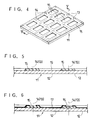
- rectangular bonding openings 16 are formed, by known photolithography for example, in the insulating film 15 at the portions thereof corresponding to the respective chip substrate segments 12.
- the photolithography includes the steps of forming a photoresist film on the upper surface of the insulating film 15, placing on the photoresist film a photomask having windows which are identical in configuration to the bonding openings 16, irradiating the masked photoresist film for subsequent development, removing the portions of the photoresist film corresponding to the windows, and etching the insulating film 15 in this condition to remove the dissolved portions thereof corresponding to the windows for thereby forming the bonding openings 16.
- a thin film 17 of tantalum silicide is formed on the master substrate 11 at each of the bonding openings 16 by sputtering for example.
- a metal layer 18 of tantalum as a bonding layer is formed on the thin film 17 similarly by sputtering for example.
- a frame layer 19 of e.g. a synthetic resin having a relatively large thickness is formed over the entire upper surface of the master substrate 11.
- shaping bores 20 are formed, by photolithography for example, in the shaping layer 19 at the portions thereof corresponding to the respective chip substrate segments 12. It should be noted however that, in place of the process steps shown in Figs. 8 through 10, a frame layer 19 having previously formed shaping bores 20 may be adhered to the master substrate 11.
- a suitable amount of tantalum powder previously mixed with a binder is loaded into each of the shaping bores 20 of the frame layer 19 and compacted for forming a porous chip 21 which is subsequently subjected to a debinder treatment wherein the binder is removed by heating for example.
- the frame layer 19 is removed by suitable means such as peeling or etching. It should be noted that the above-described binder removal may be performed after the removal of the frame layer 19.
- the master substrate 11 together with the related parts formed thereon is placed in a vacuum heating oven (not shown) and heated to the sintering temperature of tantalum under vacuum.
- the tantalum powder constituting each chip 21 is sintered while also fusing to the bonding metal layer 18, thereby electrically connecting the chip 21 to the master substrate 11.
- the thin layer 17 of tantalum silicide as a backing for the bonding metal layer 18 of tantalum performs the following function.
- tantalum within the bonding metal layer 17 abnormally diffuses into the silicon master substrate 11 due to the heat of sintering, so that the bonding strength between the chip 21 of tantalum powder and the silicon master substrate 11 will greatly reduce.
- the presence of the tantalum silicide thin layer 17 prevents diffusion of tantalum from the bonding metal layer 18 into the master substrate 11, so that the chip 21 will be bonded reliably and stably onto the master substrate 11.
- the master substrate 11 together with the related parts formed thereon is immersed in a chemical solution (not shown) such as aqueous solution of phosphoric acid to perform anodic oxidation by passing a direct current between the master substrate 11 and the chemical solution.
- a chemical solution such as aqueous solution of phosphoric acid
- a dielectric film 22 of tantalum pentoxide is formed on the surfaces of the tantalum particles of each chip 21 as well as on the exposed surfaces of the thin film 17 and bonding metal layer 18, as shown in Fig. 14, as shown in Fig. 14.
- the steps are repeated plural times which comprises immersing each chip 21 on the master substrate 11 in an aqueous solution of manganese nitrate (not shown) until the solution permeate into the chip 21, and baking the chip 21 after lifting it out of the manganese nitrate solution.
- a solid electrolyte layer 23 of manganese dioxide is formed on the surface of the tantalum pentoxide dielectric layer 22, thereby providing a capacitor element 24, as shown in Fig. 15.
- the solid electrolyte layer 23 may be made of a conductive electrolytic polymer which can be formed by chemical polymerization, electrolytic oxidizing polymerization, gas-phase polymerization or the like, as disclosed in Japanese Patent Application Laid-open Nos. 60-37114 and 1-253226 for example.
- a resin coating 25 of e.g. a polyimide or epoxy resin is formed over the entire upper surface of the master substrate 11 to cover the entire surfaces of the capacitor element 24, as shown in Fig. 16.
- a window opening 24 is formed, by photolithography for example, in the resin coating 25 at the portions thereof corresponding to the upper surface of each capacitor element 24.
- a cathode terminal electrode film 27 including a base nickel layer and an upper solder layer is formed on the upper surface of each capacitor element 24 by sputtering for example.
- the cathode terminal electrode film 27 conducts electrically with the solid electrode layer 23 via the above-described graphite layer.
- an anode terminal electrode film 28 including a base nickel layer and an upper solder layer is formed on the lower surface of each capacitor element 24 by sputtering for example.
- the master substrate 11 and the resin coating 25 are cut along the respective cutting lines 13, 14 by high-speed rotary cutters 29 for division into the respective chip substrate segments 19. As a result, a plurality of tantalum solid electrolytic capacitors are obtained.
- Figs. 20 through 22 show the structure of the tantalum solid electrolytic capacitor 30 obtained by the above-described process.
- the the tantalum solid electrolytic capacitor 30 has a width W, a length L and a high H.
- the the tantalum solid electrolytic capacitor 30 comprises a chip substrate segment 12, a sintered tantalum powder chip 21 formed on the chip substrate segment 12, and a solid electrolyte layer 23 formed on the chip 21 but electrically insulated from the tantalum particles thereof via a dielectric layer 22. Further, the capacitor 30 also includes a resin coating 25 covering the chip 21 except for a central portion of its upper surface, a cathode terminal electrode film 27 formed on the exposed portion of the solid electrolyte layer 23 in electrical conduction therewith, and an anode terminal electrode film 28 formed on the lower surface of each capacitor element 24 in electrical conduction therewith.
- the tantalum particles of the chip 21 conduct with the anode terminal electrode film 28 via the tantalum silicide thin layer 17, the bonding metal layer 18 and the chip substrate segment 12.
- electrical insulation between the anode side and cathode side of the tantalum solid electrolytic capacitor 30 is established by the insulating 15 formed on the upper surface of the chip substrate segment 12.
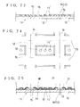
- the first embodiment of the present invention may be modified in the manner illustrated in Figs. 23 through 25. Specifically, as shown in Figs. 23 and 24, the bonding openings 15 are formed in the insulating layer 15 in a manner such that part of the insulating layer 15 remains a plurality of projections 15' in each of the bonding openings 15. As a result, the bonding metal layer 18 subsequently formed is rugged, as shown in Fig. 25.
- Figs. 26 through 34 show a second embodiment of the present invention.
- a master substrate 11a made of tantalum is first prepared which corresponds in size to a plurality of chip substrate segments 12a, and an insulating film 15a made of silicon oxide or nitride for example is formed on the master substrate 11a by thermal oxidation, PV sputtering or plasma CVD for example.
- bonding openings 16a are formed, by known photolithography for example, in the insulating film 15a at the portions thereof corresponding to the respective chip substrate segments 12a. As a result, a bonding surface 18a provided by the original surface of the master substrate 11a is exposed.
- tantalum powder is compacted into chips 21a at each of the bonding openings 16a as in the first embodiment, and after a debinder treatment the master substrate 11a is placed in a vacuum heating oven (not shown) and heated to the sintering temperature of tantalum under vacuum. As a result, the tantalum powder of each chip 21a is sintered while also fusing to the bonding surface 18a.
- steps include forming a dielectric layer 22a of tantalum pentoxide on each chip 21a (Fig. 29), forming a solid electrolyte layer 23a of manganese nitrate (Fig. 30), forming a resin coating 25a (Fig. 31) after forming a coating graphite layer (not shown) to convert the chip 21a into a capacitor element 24a, forming window openings 26a in the resin coating 25a (Fig. 32), forming a cathode terminal electrode film 27a on the upper surface of the capacitor element 24a (Fig. 33), forming an anode terminal electrode film 28a on the lower surface of the master substrate 11a (also Fig. 33), and cutting the master substrate 11a and the resin coating 25a by a high-speed rotary cutter 29a or the like (also Fig. 33).
- the foregoing process steps result in simultaneous production of a plurality of tantalum solid electrolytic capacitors 30a each having a structure which is similar to that of the first embodiment.
- the tantalum master substrate 11a since the surface of the master substrate 11a itself can be utilized as the bonding surface 18a, it is unnecessary to form a bonding metal layer of tantalum and a thin base layer of tantalum silicide on the master substrate, as opposed to the first embodiment.
- the bonding surface 18a of the master substrate 11a may be rugged, as shown in Figs. 23 through 25.
- Figs. 35 through 42 show a third embodiment of the present invention.
- a tantalum solid electrolytic capacitor 30b (Fig. 34) is manufactured by using a master substrate made of a ceramic material to which a conductive material such as BN (boron nitride) or SiC (silicon carbide) is added to impart electric conductivity.
- a conductive material such as BN (boron nitride) or SiC (silicon carbide) is added to impart electric conductivity.
- a master substrate 11b made of a conductive ceramic material is first prepared which corresponds in size to a plurality of chip substrate segments 12b, and a tantalum bonding layer 18b is formed on the master substrate 11b by sputtering for example.
- tantalum powder is compacted into chips 21b as in the first embodiment at the portions thereof corresponding to the respective chip substrate segments 12b, and after a debinder treatment the master substrate 11b is placed in a vacuum heating oven (not shown) and heated to the sintering temperature of tantalum under vacuum.
- the tantalum powder of each chip 21b is sintered while also fusing to the bonding metal layer 18b for bonding to the master substrate 11b.
- steps include forming a dielectric layer 22b of tantalum pentoxide on each chip 21b (Fig. 37), forming a solid electrolyte layer 23b of manganese nitrate (Fig. 38), forming a resin coating 25b (Fig. 39) after forming a coating graphite layer (not shown) to convert the chip 21b into a capacitor element 24b, forming window openings 26b in the resin coating 25b (Fig. 40), forming a cathode terminal electrode film 27b on the upper surface of the capacitor element 24b (Fig. 41), forming an anode terminal electrode film 28b on the lower surface of the master substrate 11b (also Fig.
- the third embodiment since an electrically conductive ceramic material is used to make the master substrate 11b, it is possible to realize a production cost decrease through saving of the material cost, as compared with the second embodiment wherein a tantalum master substrate is used.
- an insulating layer 15 or 15a may be formed on the master substrate 11b as in the first and second embodiments, and the bonding metal layer 18b on the master substrate 11b may be rugged in the same manner as shown in Figs. 23 through 25.
- Figs. 43 through 45 show a fourth embodiment of the present invention.
- a large-capacity tantalum solid electrolytic capacitor 30c is manufactured by using a master substrate 11c made of a material such as silicon, tantalum or electrically conductive ceramic which has an electric conductivity at least in its thickness direction.
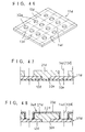
- an insulating layer 15c is formed on the master substrate 11c, and bonding openings 16c are thereafter formed in the insulating layer 15c at the portions thereof corresponding to the respective chip substrate segments 12c. Further, the master substrate 11c is formed with filling through-bores 32 at the portions thereof corresponding to the respective chip substrate segments 12c.
- a film 33 is attached to the lower surface of the master substrate 11c to close the respective filling through-bores 32, and thereafter tantalum powder is compacted into chips 21c on the master substrate 11c in a manner such that the tantalum powder also fills the respective filling through-bores 32.
- the film 33 is removed after compacting the chips 21c.
- steps are followed by the steps which are similar to those of each foregoing embodiment. These steps include sintering each of the chips 21c, forming a dielectric layer 22c on the chip 21c, forming a solid electrolyte layer 23c, forming a coating graphite layer to provide a capacitor element 24c, forming a resin coating 25c, forming a cathode terminal electrode film 27c, forming an anode terminal electrode film 28c, and cutting the master substrate 11c along the respective cutting lines for division into the respective chip substrate segments 12c. As a result of these steps, a plurality of tantalum solid electrolytic capacitors 30c each having the structure shown in Fig. 45 are produced simultaneously.
- the tantalum powder of each chip 21c also fills the filling through-bore 32, the volume of the chip 21c is correspondingly increased, thereby increasing the capacity of the tantalum solid electrolytic capacitor 30c. Further, an additional advantage is also obtainable that the bonding strength between the chip substrate segment 12c and the chip 21c is increased by the portion of the chip 21c projecting into the filling through-bore 32.
- the filling through-bore 32 may be replaced with a bottomed bore (or recess).
- the through-bore 32 makes it possible to directly and reliably bring the anode terminal electrode film 28c on the lower surface of the chip substrate segment 12c into electrical conduction with the tantalum powder of the chip 21c with the intervention of the chip substrate segment 12c. It is therefore possible to reduce the need for forming a bonding metal layer on the upper surface of the master substrate 11c as in the first and third embodiments or for providing a rugged bonding metal layer as shown in Figs. 23 through 25.
- Figs. 46 through 50 show a fifth embodiment of the present invention.
- a large-capacity tantalum solid electrolytic capacitor 30d (Fig. 50) is manufactured by using a master substrate 11d made of an insulating material such as a ceramic material.
- a master substrate 11d of an insulating ceramic material is first prepared which corresponds in size to a plurality of chip substrate segments 12d and which is formed with filling through-bores 32a at the portions thereof corresponding to the respective chip substrate segments 12d.
- a film 33a is attached to the lower surface of the master substrate 11d to close the respective filling through-bores 32a, and thereafter tantalum powder is compacted into chips 21d on the master substrate 11d in a manner such that the tantalum powder also fills the respective filling through-bores 32a.
- the film 33a is removed after compacting the chips 21d.
- steps are followed by the steps which are similar to those of each foregoing embodiment. These steps include sintering each of the chips 21d, forming a dielectric layer 22d on the chip 21d (Fig. 48), forming a solid electrolyte layer 23d (also Fig. 48), forming a coating graphite layer to provide a capacitor element 24d (also Fig. 48), forming a resin coating 25d (Fig. 49), forming a cathode terminal electrode film 27d (also Fig. 49), forming an anode terminal electrode film 28d (also Fig. 49), and cutting the master substrate 11d along the respective cutting lines 13d, 14d for division into the respective chip substrate segments 12d. As a result of these steps, a plurality of tantalum solid electrolytic capacitors 30d each having the structure shown in Fig. 50 are produced simultaneously.
- the fifth embodiment described above is similar to the fourth embodiment in that the tantalum powder of th chip 21d which fills the filling through-bore 32a increases the capacity of the tantalum solid electrolytic capacitor 30d.
- the chip substrate segment 12d is made of an insulating material such as ceramic material, the anode and cathode sides of the capacitor element 24d can be reliably insulated electrically without separately providing an insulating layer on the chip substrate segment 12d, thereby providing an advantage of realizing a cost and weight reduction in comparison with the case wherein the chip substrate segment 12d is made of a conductive material.
- Figs. 51 through 56 show a sixth embodiment of the present invention.
- a large-capacity tantalum solid electrolytic capacitor 30e (Fig. 56) is manufactured by using a master substrate 11e made of an insulating material such as a ceramic material as in the fifth embodiment.
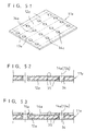
- a master substrate 11e of an insulating ceramic material is first prepared which corresponds in size to a plurality of chip substrate segments 12e and which is formed with conduction through-bores 34 between the respective chip substrate segments 12e.
- a metal layer 35 of e.g. tantalum is formed on the upper and lower surfaces of the master substrate and the inner surfaces of the respective conduction through-bores 34.
- an insulating layer 15e is formed on the upper surface of the master substrate 11e, and bonding openings 16e are formed in the insulating layer 15e.
- tantalum powder is compacted into chips 21e on the master substrate 11e.
- steps are followed by the steps which are similar to those of each foregoing embodiment. These steps include sintering each of the chips 21e, forming a dielectric layer 22e on the chip 21e (Fig. 55), forming a solid electrolyte layer 23e (also Fig. 55), forming a coating graphite layer to provide a capacitor element 24e (also Fig. 55), forming a resin coating 25e (also Fig. 55), forming a cathode terminal electrode film 27e (also Fig. 55), forming an anode terminal electrode film 28e (also Fig. 55), and cutting the master substrate 11e along the respective cutting lines 13e, 14e for division into the respective chip substrate segments 12e. As a result of these steps, a plurality of tantalum solid electrolytic capacitors 30e each having the structure shown in Fig. 56 are produced simultaneously.
- the chip substrate segment 12e is made of an inexpesive insulating material, it is possible to reliably establish electrical connection between the anode terminal electrode film 28e on the lower surface of the chip substrate segment and the tantalum particles of the chip 21e via the metal layer 35 formed on the chip substrate segment 12e.
Landscapes
- Engineering & Computer Science (AREA)
- Power Engineering (AREA)
- Microelectronics & Electronic Packaging (AREA)
- Fixed Capacitors And Capacitor Manufacturing Machines (AREA)
- Parts Printed On Printed Circuit Boards (AREA)
Abstract
Description
- This invention relates generally to solid electrolytic capacitors such as tantalum capacitors. More specifically, the present invention relates to a solid electrolytic capacitor which is suitably designed for surface mounting. The present invention also relates to a process for making such a solid electrolytic capacitor.
- Conventionally, a capacitor element for use in a solid electrolytic capacitor of this type was most typically manufactured in the following manner.
- First, as shown in Fig. 57 of the accompanying drawings, metal powder such as tantalum powder is compacted into a
porous chip 2 from which ametal anode wire 3 made of e.g. tantalum projects out and thereafter sintered. - Then, as shown in Fig. 58, the
chip 2 is immersed in a chemical solution A such as aqueous solution of phosphoric acid, and a direct current is passed between theanode wire 3 and the solution A for performing anodic oxidation. As a result, adielectric film 4 of tantalum pentoxide for example is formed on the surfaces of the metal particles of thechip 2. - Then, as shown in Fig. 59, the steps are repeated plural times which comprise immersing the
chip 2 in an aqueous solution B of manganese nitrate until the manganese nitrate solution B permeates into thechip 2, and thereafter lifting out the chip for baking. As a result, asolid electrolyte layer 5 of a metal oxide such as manganese dioxide is formed on the surface of thedielectric film 4. - Finally, a cathode film made of a metal such as silver or nickel is formed after graphitizing the surface of the
solid electrolyte layer 5 of thechip 2. This provides acapacitor element 1. - As described above, in making the
capacitor element 1 for the prior art solid electrolytic capacitor, theanode wire 3 projecting from thechip 2 is indispensable and cannot be obviated. Therefore, it was conventional to employ the structure of Fig. 60 or 61 for making a surface-mounting type solid electrolytic capacitor by incorporating thecapacitor element 1. - Specifically, according to the structure shown in Fig. 60, the
capacitor element 1 is arranged between acathode lead terminal 6a and ananode lead terminal 6b. Thechip 2 of thecapacitor element 1 is attached to thecathode lead terminal 6b, whereas theanode wire 3 is attached to theanode lead terminal 6a. Thecapacitor element 1 together with the inner ends of therespective lead terminals synthetic resin package 7. The solid electrolytic capacitor of such a structure is disclosed in Japanese Patent Application Laid-open No. 60-220922 for example. - According to the structure shown in Fig. 61, on the other hand, the
capacitor element 1 is enclosed in a moldedsynthetic resin package 8 in a manner such that the tip portion of theanode wire 3 and the end face of thechip 2 opposite to theanode wire 3 are exposed. The exposed tip portion of theanode wire 3 is formed with ananode terminal portion 9a made of e.g. solder, whereas the exposed end face of the chip is formed with acathode terminal portion 9b made of e.g. solder. - However, in either one of the above-described solid electrolytic capacitors, the
capacitor element 1 need be enclosed in the resin package7, 8 in such a manner as to contain both thechip 2 and the projectinganode wire 3. Therefore, thepackage chip 2 of thecapacitor element 1 by as much as theanode wire 3 projects out from thechip 2, so that the ratio of the volume of thechip 2 relative to the overall volume of the capacitor decreases to result in a volume efficiency reduction. Further, the effective volume of thechip 2 also reduces by as much as theanode wire 3 is embedded in thechip 2. Due to these factors, the prior art solid electrolytic capacitor poses difficulty in increasing the capacitance per unit volume while also giving rise to a weight increase problem. These problems are particularly remarkable with respect the solid electrolytic capacitor having the structure of Figs. 60 which incorporates the twolead terminals - Additionally, in each of the solid electrolytic capacitors, large stresses are applied to the
chip 2 when molding theresin package - Further, when conventionally making a plurality of
capacitor elements 1 at a time, each of the projectinganode wires 3 of plural sinteredchips 1 is attached to ametal bar 10 of e.g. tantalum, as shown in Fig. 62. In this condition, various process steps are performed which include forming thedielectric layer 4 by immersion in the chemical solution A (Fig. 58), forming thesolid electrolyte layer 5 by immersion in the aqueous solution B of manganese nitrate (Fig. 59), graphitizing, forming the cathode film, and the like. After these steps, each of thecapacitor elements 1 is cut off themetal bar 10. Therefore, there is a limitation in the number ofcapacitor elements 1 which can be produced by using thesingle metal bar 10, so that there is difficulty in meeting the requirements for mass production. Thus, combined with a low yield of production, a production cost will result. - In particular, since the solid electrolytic capacitor of the type shown in Fig. 60 incorporates the two
lead terminals respective lead terminals capacitor element 1 and bending thelead terminals - It is, therefore, an object of the present invention to provide a surface mounting type solid electrolytic capacitor which overcomes the above-described problems.
- Another object of the present invention is to provide a process for making such a solid electrolytic capacitor.
- According to a first aspect of the present invention, there is provided a solid electrolytic capacitor comprising: a chip substrate segment; a sintered chip of metal powder mounted on an upper surface of the chip substrate segment; a solid electrolyte layer formed on the chip in electrical insulation from the metal powder of the chip via a dielectric film; a resin coating covering the chip with a portion of the solid electrolyte layer exposed; a cathode terminal electrode film formed in electrical conduction with the exposed portion of the solid electrolyte layer; and an anode terminal electrode film formed on the chip substrate segment in electrical conduction with the metal powder of the chip.
- With the arrangement described above, it is only necessary to cover the side surfaces of the capacitor element with the resin coating, and an anode wire projecting from the chip may be obviated. Therefore, since the effective volume of the chip will not be decreased due to the presence of the anode wire, the ratio of the volume of the chip relative to the overall volume can be reliably increased in comparison with a conventional solid electrolytic capacitor having an anode wire, thereby realizing an improvement of space efficiency and a size reduction. In particular, a great size and weight reduction is obtainable over the solid electrolytic capacitor of the type which has metal plate lead terminals as shown in Fig. 60.
- The chip substrate segment may be formed with a filling bore extending from the upper surface thereof, and the metal powder of the chip may be made to fill in the filling bore. This arrangement leads to a volume increase of the chip to additionally enhance the volume efficiency, thereby increasing the capacitance of the solid electrolytic capacitor per unit volume. In particular, in case where the filling bore is a through-bore, a portion of the metal powder filled in the through-bore is directly bonded to the anode terminal electrode film on the lower surface of the chip substrate segment, thereby providing an additional volume increase of the chip while also improving reliability of electrical conduction between the metal powder of the chip and the anode terminal electrode film.
- The chip substrate segment may be made of a material which has electrical conductivity at least in a thickness direction of the chip substrate segment, and the metal powder of the chip may be electrically connected to the chip substrate chip with the anode terminal electrode film formed on the chip substrate chip. In this case, since the chip substrate segment itself takes the place of a conventional anode wire and is therefore effective in enhancing the volume efficiency. Further, if an insulating layer is formed on the upper surface of the chip substrate segment to surround the chip, it electrically insulates between the chip substrate segment and the solid electrolyte layer, thereby reliably preventing current leakage between the two.
- According to a second aspect of the present invention, there is provided a process for making solid electrolytic capacitors comprising the steps of: preparing a master substrate corresponding in size to a plurality of chip substrate segments; compacting metal powder on an upper surface of the master substrate into porous chips at positions corresponding to the chip substrate segments; heating each of the chips for sintering; forming a dielectric layer on each said chip of metal powder; forming a solid electrolyte layer on the dielectric layer; applying a resin coating at least on side surfaces of said each chip; forming a cathode terminal electrode film on the solid electrolyte layer of each said chip, while also forming an anode terminal layer on a lower surface of the master substrate at least at positions corresponding to the chip substrate segments; and cutting the master substrate between the chips for division into the respective chip substrate segments.
- With the process described above, the step of compacting the metal powder into the chips and the step of heating the chips for sintering can be performed simultaneously with respect to plural items by using the single master substrate. In addition, the subsequent steps of forming the dielectric film, the solid electrolyte layer, the resin coating, the anode terminal electrode film and the cathode terminal electrode film can also be performed under the condition wherein the plural chips are bonded to the master substrate. Finally, the master substrate need only be cut between the respective chips for division into the respective chip substrate segments, thereby yielding a plurality of surface-mounting type solid electrolytic capacitors at one time. Therefore, the manufacturing process of the present invention is more suitable for mass production than the prior art process wherein a plurality of solid electrolytic capacitors are separately manufactured.
- In addition, by applying the resin coating at least on the side surfaces of each chip, it is possible to reliably decrease the likelihood of increasing the leak current (LC) and insulation failure occurrence. Thus, combined with the above-described suitability for mass production, the process of the present invention which is capable of decreasing the occurrence of rejectable products is advantageous in greatly reducing the production cost.
- Various features and advantages of the present invention will be become apparent from the following description of the preferred embodiments given with reference to the accompanying drawings.
-
- Fig. 1 is a perspective view showing a master substrate for use in a first embodiment of the present invention;
- Fig. 2 is a perspective view showing the same master substrate which is formed with an insulating layer;
- Fig. 3 is an enlarged sectional view taken along lines III-III in Fig. 2;
- Fig. 4 is a perspective view showing the state wherein the insulating layer of the same master substrate is formed with bonding openings;
- Fig. 5 is an enlarged sectional view taken along lines V-V in Fig. 4;
- Fig. 6 is an enlarged sectional view showing the state wherein a thin film of tantalum silicide is formed in the bonding openings according to the first embodiment;
- Fig. 7 is an enlarged sectional view showing the state wherein a bonding metal layer is formed on the thin film of tantalum silicide;
- Fig. 8 is an enlarged sectional view showing the state wherein a frame layer is formed on the same master substrate according to the first embodiment;
- Fig. 9 is a perspective view showing the state wherein shaping bores are formed in the frame layer;
- Fig. 10 is an enlarged sectional view taken along lines X-X in Fig. 9;
- Fig. 11 is an enlarged sectional view showing the state wherein tantalum powder is compacted into chips in the shaping bores of the frame layer;
- Fig. 12 is a perspective view showing the state wherein the frame layer has been removed in the first embodiment;
- Fig. 13 is an enlarged sectional view taken along lines XIII-XIII in Fig. 12;
- Fig. 14 is an enlarged sectional view showing the state wherein a dielectric layer has been formed on the chips according to the first embodiment;
- Fig. 15 is an enlarged sectional view showing the state wherein a solid electrolyte layer has been formed on the chips according to the first embodiment;
- Fig. 16 is an enlarged sectional view showing the state wherein a resin coating has been formed on the master substrate according to the first embodiment;
- Fig. 17 is a perspective view showing the state wherein window openings have been formed in the resin coating according to the first embodiment;
- Fig. 18 is an enlarged sectional view taken along lines XVIII-XVIII in Fig. 17;
- Fig. 19 is a perspective view showing the state wherein a cathode terminal electrode film and an anode terminal electrode film have been formed according to the first embodiment;
- Fig. 20 is a perspective view showing a solid electrolytic capacitor made according to the first embodiment;
- Fig. 21 is an enlarged sectional view taken along lines XXI-XXI in Fig. 20;
- Fig. 22 is an enlarged sectional view taken along lines XXII-XXII in Fig. 20;
- Fig. 23 is an enlarged sectional view showing a principal portion of a modification of the first embodiment;
- Fig. 24 is a plan view showing the modification of Fig. 23;
- Fig. 25 is an enlarged sectional view showing the state wherein a thin layer of tantalum silicide and a bonding metal layer have been formed in the modification of Fig. 23;
- Fig. 26 is an enlarged sectional view showing a master substrate for use in a second embodiment of the present invention;
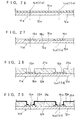
- Fig. 27 is an enlarged sectional view showing the state wherein bonding openings has been formed in an insulating layer according to the second embodiment;
- Fig. 28 is an enlarged sectional view showing the state wherein chips have been compacted on the master substrate according to the second embodiment;
- Fig. 29 is an enlarged sectional view showing the state wherein a dielectric layer has been formed on the chips according to the second embodiment;
- Fig. 30 is an enlarged sectional view showing the state wherein a solid electrolyte layer has been formed on the chips according to the second embodiment;
- Fig. 31 is an enlarged sectional view showing the state wherein a resin coating have been formed on the master substrate according to the second embodiment;
- Fig. 32 is an enlarged sectional view showing the state wherein window openings have been formed in the resin coating according to the second embodiment;
- Fig. 33 is an enlarged sectional view showing the state wherein a cathode terminal electrode film and an anode terminal electrode film have been formed according to the second embodiment;
- Fig. 34 is an enlarged sectional view showing a solid electrolytic capacitor made according to the second embodiment;
- Fig. 35 is an enlarged sectional view showing a master substrate for use in a third embodiment of the present invention;
- Fig. 36 is an enlarged sectional view showing the state wherein chips have been compacted on the master substrate according to the third embodiment;
- Fig. 37 is an enlarged sectional view showing the state wherein a dielectric layer has been formed on the chips according to the third embodiment;
- Fig. 38 is an enlarged sectional view showing the state wherein a solid electrolyte layer has been formed on the chips according to the third embodiment;
- Fig. 39 is an enlarged sectional view showing the state wherein a resin coating have been formed on the master substrate according to the third embodiment;
- Fig. 40 is an enlarged sectional view showing the state wherein window openings have been formed in the resin coating according to the third embodiment;
- Fig. 41 is an enlarged sectional view showing the state wherein a cathode terminal electrode film and an anode terminal electrode film have been formed according to the third embodiment;
- Fig. 42 is an enlarged sectional view showing a solid electrolytic capacitor made according to the third embodiment;
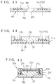
- Fig. 43 is an enlarged sectional view showing a master substrate for use in a fourth embodiment of the present invention;
- Fig. 44 is an enlarged sectional view showing the state wherein chips have been compacted on the master substrate according to the fourth embodiment;
- Fig. 45 is an enlarged sectional view showing a solid electrolytic capacitor made according to the fourth embodiment;
- Fig. 46 is a perspective view showing a master substrate for use in a fifth embodiment of the present invention;
- Fig. 47 is an enlarged sectional view showing the state wherein chips have been compacted on the upper surface of the master substrate according to the fifth embodiment;
- Fig. 48 is an enlarged sectional view showing the state wherein a dielectric layer and a solid electrolyte layer have been formed on the chips according to the fifth embodiment;
- Fig. 49 is an enlarged sectional view showing the state wherein a resin coating, a cathode terminal electrode film and an anode terminal electrode film have been formed according to the fifth embodiment;
- Fig. 50 is an enlarged sectional view showing a solid electrolytic capacitor made according to the fifth embodiment;
- Fig. 51 is a perspective view showing a master substrate for use in a sixth embodiment of the present invention;
- Fig. 52 is an enlarged sectional view showing the state wherein a metal film has been formed on the master substrate according to the sixth embodiment;
- Fig. 53 is an enlarged sectional view showing the state wherein an insulating layer has been formed on the master substrate according to the sixth embodiment;
- Fig. 54 is an enlarged sectional view showing the state wherein chips have been compacted on the master substrate according to the sixth embodiment;
- Fig. 55 is an enlarged sectional view showing the state wherein a dielectric layer, a solid electrolyte layer, a resin coating, a cathode terminal electrode film and an anode terminal electrode film have been formed according to the sixth embodiment;
- Fig. 56 is an enlarged sectional view showing a solid electrolytic capacitor made according to the sixth embodiment;
- Fig. 57 is a perspective view showing a capacitor element for use in making a prior art solid electrolytic capacitor;
- Fig. 58 is a view showing the process step of forming a dielectric layer on the capacitor element of Fig. 57;
- Fig. 59 is a view showing the process step of forming a solid electrolyte layer on the capacitor element of Fig. 57;
- Fig. 60 is a sectional front view showing a prior art solid electrolytic capacitor;
- Fig. 61 is a sectional front view showing another prior art solid electrolytic capacitor; and
- Fig. 62 is a perspective view showing the state wherein capacitor elements are attached to a metal bar in the process of making prior art solid electrolytic capacitors.
- Embodiments of the present invention are described below with reference to the accompanying drawings.
- Figs. 1 through 22 show a first embodiment of the present invention. In this embodiment, a tantalum solid electrolytic capacitor 30 (Fig. 20) is manufactured by using a master substrate made of silicon.
- According to the first embodiment, a
master substrate 11 made of silicon is first prepared which has electric conductivity in the thickness direction, as shown in Fig. 1. Themaster substrate 11 corresponds in size to a plurality ofchip substrate segments 12 each of which is rectangular with a width W and a length L. As described hereinafter, themaster substrate 11 provides the plurality ofchip substrate segments 12 when cut alonglongitudinal cutting lines 13 andtransverse cutting lines 14 in the final process step. - Then, as shown in Figs. 2 and 3, an insulating
film 15 made of silicon oxide or nitride for example is formed on themaster substrate 11 by thermal oxidation, PV sputtering or plasma CVD for example. - Then, as shown in Figs. 4 and 5,
rectangular bonding openings 16 are formed, by known photolithography for example, in the insulatingfilm 15 at the portions thereof corresponding to the respectivechip substrate segments 12. The photolithography includes the steps of forming a photoresist film on the upper surface of the insulatingfilm 15, placing on the photoresist film a photomask having windows which are identical in configuration to thebonding openings 16, irradiating the masked photoresist film for subsequent development, removing the portions of the photoresist film corresponding to the windows, and etching the insulatingfilm 15 in this condition to remove the dissolved portions thereof corresponding to the windows for thereby forming thebonding openings 16. - Then, as shown in Fig. 6, a
thin film 17 of tantalum silicide is formed on themaster substrate 11 at each of thebonding openings 16 by sputtering for example. - Then, as shown in Fig. 7, a
metal layer 18 of tantalum as a bonding layer is formed on thethin film 17 similarly by sputtering for example. - Then, as shown in Fig. 8, a
frame layer 19 of e.g. a synthetic resin having a relatively large thickness is formed over the entire upper surface of themaster substrate 11. - Then, as shown in Figs. 9 and 10, shaping bores 20 are formed, by photolithography for example, in the
shaping layer 19 at the portions thereof corresponding to the respectivechip substrate segments 12. It should be noted however that, in place of the process steps shown in Figs. 8 through 10, aframe layer 19 having previously formed shaping bores 20 may be adhered to themaster substrate 11. - Then, as shown in Fig. 11, a suitable amount of tantalum powder previously mixed with a binder is loaded into each of the shaping bores 20 of the
frame layer 19 and compacted for forming aporous chip 21 which is subsequently subjected to a debinder treatment wherein the binder is removed by heating for example. - Then, as shown in Figs. 12 and 13, the
frame layer 19 is removed by suitable means such as peeling or etching. It should be noted that the above-described binder removal may be performed after the removal of theframe layer 19. - Then, the
master substrate 11 together with the related parts formed thereon is placed in a vacuum heating oven (not shown) and heated to the sintering temperature of tantalum under vacuum. As a result, the tantalum powder constituting eachchip 21 is sintered while also fusing to thebonding metal layer 18, thereby electrically connecting thechip 21 to themaster substrate 11. In this sintering step, thethin layer 17 of tantalum silicide as a backing for thebonding metal layer 18 of tantalum performs the following function. Specifically, absent thethin layer 17 of tantalum silicide, tantalum within thebonding metal layer 17 abnormally diffuses into thesilicon master substrate 11 due to the heat of sintering, so that the bonding strength between thechip 21 of tantalum powder and thesilicon master substrate 11 will greatly reduce. By contrast, the presence of the tantalum silicidethin layer 17 prevents diffusion of tantalum from thebonding metal layer 18 into themaster substrate 11, so that thechip 21 will be bonded reliably and stably onto themaster substrate 11. - Then, the
master substrate 11 together with the related parts formed thereon is immersed in a chemical solution (not shown) such as aqueous solution of phosphoric acid to perform anodic oxidation by passing a direct current between themaster substrate 11 and the chemical solution. As a result, adielectric film 22 of tantalum pentoxide is formed on the surfaces of the tantalum particles of eachchip 21 as well as on the exposed surfaces of thethin film 17 andbonding metal layer 18, as shown in Fig. 14, as shown in Fig. 14. - Then, the steps are repeated plural times which comprises immersing each
chip 21 on themaster substrate 11 in an aqueous solution of manganese nitrate (not shown) until the solution permeate into thechip 21, and baking thechip 21 after lifting it out of the manganese nitrate solution. As a result, asolid electrolyte layer 23 of manganese dioxide is formed on the surface of the tantalumpentoxide dielectric layer 22, thereby providing acapacitor element 24, as shown in Fig. 15. It should be noted that thesolid electrolyte layer 23 may be made of a conductive electrolytic polymer which can be formed by chemical polymerization, electrolytic oxidizing polymerization, gas-phase polymerization or the like, as disclosed in Japanese Patent Application Laid-open Nos. 60-37114 and 1-253226 for example. - Then, after forming a coating graphite layer (not shown) over the entire surface of each
capacitor element 24, aresin coating 25 of e.g. a polyimide or epoxy resin is formed over the entire upper surface of themaster substrate 11 to cover the entire surfaces of thecapacitor element 24, as shown in Fig. 16. - Then, as shown in Figs. 17 and 18, a
window opening 24 is formed, by photolithography for example, in theresin coating 25 at the portions thereof corresponding to the upper surface of eachcapacitor element 24. - Then, as shown in Fig. 19, a cathode
terminal electrode film 27 including a base nickel layer and an upper solder layer is formed on the upper surface of eachcapacitor element 24 by sputtering for example. The cathodeterminal electrode film 27 conducts electrically with thesolid electrode layer 23 via the above-described graphite layer. - On the other hand, as also shown in Fig. 19, an anode
terminal electrode film 28 including a base nickel layer and an upper solder layer is formed on the lower surface of eachcapacitor element 24 by sputtering for example. - Finally, as also shown in Fig. 19, the
master substrate 11 and theresin coating 25 are cut along therespective cutting lines speed rotary cutters 29 for division into the respectivechip substrate segments 19. As a result, a plurality of tantalum solid electrolytic capacitors are obtained. - Figs. 20 through 22 show the structure of the tantalum solid
electrolytic capacitor 30 obtained by the above-described process. The the tantalum solidelectrolytic capacitor 30 has a width W, a length L and a high H. - The the tantalum solid
electrolytic capacitor 30 comprises achip substrate segment 12, a sinteredtantalum powder chip 21 formed on thechip substrate segment 12, and asolid electrolyte layer 23 formed on thechip 21 but electrically insulated from the tantalum particles thereof via adielectric layer 22. Further, thecapacitor 30 also includes aresin coating 25 covering thechip 21 except for a central portion of its upper surface, a cathodeterminal electrode film 27 formed on the exposed portion of thesolid electrolyte layer 23 in electrical conduction therewith, and an anodeterminal electrode film 28 formed on the lower surface of eachcapacitor element 24 in electrical conduction therewith. The tantalum particles of thechip 21 conduct with the anodeterminal electrode film 28 via the tantalum silicidethin layer 17, thebonding metal layer 18 and thechip substrate segment 12. On the other hand, electrical insulation between the anode side and cathode side of the tantalum solidelectrolytic capacitor 30 is established by the insulating 15 formed on the upper surface of thechip substrate segment 12. - The first embodiment of the present invention may be modified in the manner illustrated in Figs. 23 through 25. Specifically, as shown in Figs. 23 and 24, the
bonding openings 15 are formed in the insulatinglayer 15 in a manner such that part of the insulatinglayer 15 remains a plurality of projections 15' in each of thebonding openings 15. As a result, thebonding metal layer 18 subsequently formed is rugged, as shown in Fig. 25. - According to the above-described modification, it is possible to increase the contact area between the tantalum powder of the
chip 21 of thecapacitor element 24 and the bonding metal layer 18 (bonding layer). This improves the bonding strength and reliability when bonding thechip 21 to themaster substrate 11 simultaneously with sintering thechip 21. - Figs. 26 through 34 show a second embodiment of the present invention. In this embodiment, use is made of a tantalum master substrate for making a tantalum solid
electrolytic capacitor 30a (Fig. 34). - According to the second embodiment, as shown in Fig. 26, a
master substrate 11a made of tantalum is first prepared which corresponds in size to a plurality ofchip substrate segments 12a, and an insulatingfilm 15a made of silicon oxide or nitride for example is formed on themaster substrate 11a by thermal oxidation, PV sputtering or plasma CVD for example. - Then, as shown in Fig. 27, bonding openings 16a are formed, by known photolithography for example, in the insulating
film 15a at the portions thereof corresponding to the respectivechip substrate segments 12a. As a result, abonding surface 18a provided by the original surface of themaster substrate 11a is exposed. - Then, as shown in Fig. 28, tantalum powder is compacted into
chips 21a at each of the bonding openings 16a as in the first embodiment, and after a debinder treatment themaster substrate 11a is placed in a vacuum heating oven (not shown) and heated to the sintering temperature of tantalum under vacuum. As a result, the tantalum powder of eachchip 21a is sintered while also fusing to thebonding surface 18a. - The above-described steps are followed by the steps which are similar to those of the first embodiment. These steps include forming a
dielectric layer 22a of tantalum pentoxide on eachchip 21a (Fig. 29), forming asolid electrolyte layer 23a of manganese nitrate (Fig. 30), forming aresin coating 25a (Fig. 31) after forming a coating graphite layer (not shown) to convert thechip 21a into acapacitor element 24a, formingwindow openings 26a in theresin coating 25a (Fig. 32), forming a cathodeterminal electrode film 27a on the upper surface of thecapacitor element 24a (Fig. 33), forming an anodeterminal electrode film 28a on the lower surface of themaster substrate 11a (also Fig. 33), and cutting themaster substrate 11a and theresin coating 25a by a high-speed rotary cutter 29a or the like (also Fig. 33). - As shown in Fig. 34, the foregoing process steps result in simultaneous production of a plurality of tantalum solid
electrolytic capacitors 30a each having a structure which is similar to that of the first embodiment. However, due to the use of thetantalum master substrate 11a in the second embodiment, since the surface of themaster substrate 11a itself can be utilized as thebonding surface 18a, it is unnecessary to form a bonding metal layer of tantalum and a thin base layer of tantalum silicide on the master substrate, as opposed to the first embodiment. - In the second embodiment, the
bonding surface 18a of themaster substrate 11a may be rugged, as shown in Figs. 23 through 25. - Figs. 35 through 42 show a third embodiment of the present invention. In the third embodiment, a tantalum solid electrolytic capacitor 30b (Fig. 34) is manufactured by using a master substrate made of a ceramic material to which a conductive material such as BN (boron nitride) or SiC (silicon carbide) is added to impart electric conductivity.
- Specifically, according to the third embodiment, as shown in Fig. 35, a
master substrate 11b made of a conductive ceramic material is first prepared which corresponds in size to a plurality ofchip substrate segments 12b, and a tantalum bonding layer 18b is formed on themaster substrate 11b by sputtering for example. - Then, as shown in Fig. 36, tantalum powder is compacted into
chips 21b as in the first embodiment at the portions thereof corresponding to the respectivechip substrate segments 12b, and after a debinder treatment themaster substrate 11b is placed in a vacuum heating oven (not shown) and heated to the sintering temperature of tantalum under vacuum. As a result, the tantalum powder of eachchip 21b is sintered while also fusing to the bonding metal layer 18b for bonding to themaster substrate 11b. - The above-described steps are followed by the steps which are similar to those of the first embodiment. These steps include forming a
dielectric layer 22b of tantalum pentoxide on eachchip 21b (Fig. 37), forming asolid electrolyte layer 23b of manganese nitrate (Fig. 38), forming aresin coating 25b (Fig. 39) after forming a coating graphite layer (not shown) to convert thechip 21b into acapacitor element 24b, formingwindow openings 26b in theresin coating 25b (Fig. 40), forming a cathodeterminal electrode film 27b on the upper surface of thecapacitor element 24b (Fig. 41), forming an anodeterminal electrode film 28b on the lower surface of themaster substrate 11b (also Fig. 41), and cutting themaster substrate 11b and theresin coating 25b by a high-speed rotary cutter 29b or the like (also Fig. 41). As a result of these steps, a plurality of tantalum solid electrolytic capacitors 30b are produced simultaneously, as shown in Fig. 42. - According to the third embodiment, since an electrically conductive ceramic material is used to make the
master substrate 11b, it is possible to realize a production cost decrease through saving of the material cost, as compared with the second embodiment wherein a tantalum master substrate is used. - Again, in the third embodiment, an insulating
layer master substrate 11b as in the first and second embodiments, and the bonding metal layer 18b on themaster substrate 11b may be rugged in the same manner as shown in Figs. 23 through 25. - Figs. 43 through 45 show a fourth embodiment of the present invention. In the fourth embodiment, a large-capacity tantalum solid electrolytic capacitor 30c is manufactured by using a
master substrate 11c made of a material such as silicon, tantalum or electrically conductive ceramic which has an electric conductivity at least in its thickness direction. - Specifically, as shown in Fig. 43, an insulating
layer 15c is formed on themaster substrate 11c, andbonding openings 16c are thereafter formed in the insulatinglayer 15c at the portions thereof corresponding to the respectivechip substrate segments 12c. Further, themaster substrate 11c is formed with filling through-bores 32 at the portions thereof corresponding to the respectivechip substrate segments 12c. - Then, as shown in Fig. 44, a
film 33 is attached to the lower surface of themaster substrate 11c to close the respective filling through-bores 32, and thereafter tantalum powder is compacted intochips 21c on themaster substrate 11c in a manner such that the tantalum powder also fills the respective filling through-bores 32. Thefilm 33 is removed after compacting thechips 21c. - The above-described steps are followed by the steps which are similar to those of each foregoing embodiment. These steps include sintering each of the
chips 21c, forming a dielectric layer 22c on thechip 21c, forming asolid electrolyte layer 23c, forming a coating graphite layer to provide a capacitor element 24c, forming aresin coating 25c, forming a cathodeterminal electrode film 27c, forming an anodeterminal electrode film 28c, and cutting themaster substrate 11c along the respective cutting lines for division into the respectivechip substrate segments 12c. As a result of these steps, a plurality of tantalum solid electrolytic capacitors 30c each having the structure shown in Fig. 45 are produced simultaneously. - According to the fourth embodiment described above, since the tantalum powder of each
chip 21c also fills the filling through-bore 32, the volume of thechip 21c is correspondingly increased, thereby increasing the capacity of the tantalum solid electrolytic capacitor 30c. Further, an additional advantage is also obtainable that the bonding strength between thechip substrate segment 12c and thechip 21c is increased by the portion of thechip 21c projecting into the filling through-bore 32. - In the fourth embodiment, the filling through-
bore 32 may be replaced with a bottomed bore (or recess). However, the through-bore 32 makes it possible to directly and reliably bring the anodeterminal electrode film 28c on the lower surface of thechip substrate segment 12c into electrical conduction with the tantalum powder of thechip 21c with the intervention of thechip substrate segment 12c. It is therefore possible to reduce the need for forming a bonding metal layer on the upper surface of themaster substrate 11c as in the first and third embodiments or for providing a rugged bonding metal layer as shown in Figs. 23 through 25. - Figs. 46 through 50 show a fifth embodiment of the present invention. In the fifth embodiment, a large-capacity tantalum solid
electrolytic capacitor 30d (Fig. 50) is manufactured by using amaster substrate 11d made of an insulating material such as a ceramic material. - In the fifth embodiment, as shown in Fig. 46, a
master substrate 11d of an insulating ceramic material is first prepared which corresponds in size to a plurality ofchip substrate segments 12d and which is formed with filling through-bores 32a at the portions thereof corresponding to the respectivechip substrate segments 12d. - Then, as shown in Fig. 47, a
film 33a is attached to the lower surface of themaster substrate 11d to close the respective filling through-bores 32a, and thereafter tantalum powder is compacted intochips 21d on themaster substrate 11d in a manner such that the tantalum powder also fills the respective filling through-bores 32a. Thefilm 33a is removed after compacting thechips 21d. - The above-described steps are followed by the steps which are similar to those of each foregoing embodiment. These steps include sintering each of the
chips 21d, forming adielectric layer 22d on thechip 21d (Fig. 48), forming asolid electrolyte layer 23d (also Fig. 48), forming a coating graphite layer to provide acapacitor element 24d (also Fig. 48), forming aresin coating 25d (Fig. 49), forming a cathodeterminal electrode film 27d (also Fig. 49), forming an anodeterminal electrode film 28d (also Fig. 49), and cutting themaster substrate 11d along therespective cutting lines chip substrate segments 12d. As a result of these steps, a plurality of tantalum solidelectrolytic capacitors 30d each having the structure shown in Fig. 50 are produced simultaneously. - The fifth embodiment described above is similar to the fourth embodiment in that the tantalum powder of
th chip 21d which fills the filling through-bore 32a increases the capacity of the tantalum solidelectrolytic capacitor 30d. In addition, according to the fifth embodiment, since thechip substrate segment 12d is made of an insulating material such as ceramic material, the anode and cathode sides of thecapacitor element 24d can be reliably insulated electrically without separately providing an insulating layer on thechip substrate segment 12d, thereby providing an advantage of realizing a cost and weight reduction in comparison with the case wherein thechip substrate segment 12d is made of a conductive material. - Figs. 51 through 56 show a sixth embodiment of the present invention. In the sixth embodiment, a large-capacity tantalum solid electrolytic capacitor 30e (Fig. 56) is manufactured by using a
master substrate 11e made of an insulating material such as a ceramic material as in the fifth embodiment. - According to the sixth embodiment, as shown in Fig. 51, a
master substrate 11e of an insulating ceramic material is first prepared which corresponds in size to a plurality ofchip substrate segments 12e and which is formed with conduction through-bores 34 between the respectivechip substrate segments 12e. - Then, as shown in Fig. 52, a
metal layer 35 of e.g. tantalum is formed on the upper and lower surfaces of the master substrate and the inner surfaces of the respective conduction through-bores 34. - Then, as shown in Fig. 53, an insulating
layer 15e is formed on the upper surface of themaster substrate 11e, andbonding openings 16e are formed in the insulatinglayer 15e. - Then, as shown in Fig. 54, tantalum powder is compacted into
chips 21e on themaster substrate 11e. - The above-described steps are followed by the steps which are similar to those of each foregoing embodiment. These steps include sintering each of the
chips 21e, forming adielectric layer 22e on thechip 21e (Fig. 55), forming asolid electrolyte layer 23e (also Fig. 55), forming a coating graphite layer to provide acapacitor element 24e (also Fig. 55), forming aresin coating 25e (also Fig. 55), forming a cathodeterminal electrode film 27e (also Fig. 55), forming an anodeterminal electrode film 28e (also Fig. 55), and cutting themaster substrate 11e along therespective cutting lines chip substrate segments 12e. As a result of these steps, a plurality of tantalum solid electrolytic capacitors 30e each having the structure shown in Fig. 56 are produced simultaneously. - According to the sixth embodiment described above, while the
chip substrate segment 12e is made of an inexpesive insulating material, it is possible to reliably establish electrical connection between the anodeterminal electrode film 28e on the lower surface of the chip substrate segment and the tantalum particles of thechip 21e via themetal layer 35 formed on thechip substrate segment 12e.
Claims (18)
- A solid electrolytic capacitor comprising:a chip substrate segment;a sintered chip of metal powder mounted on an upper surface of the chip substrate segment;a solid electrolyte layer formed on the chip in electrical insulation from the metal powder of the chip via a dielectric film;a resin coating covering the chip with a portion of the solid electrolyte layer exposed;a cathode terminal electrode film formed in electrical conduction with the exposed portion of the solid electrolyte layer; andan anode terminal electrode film formed on the chip substrate segment in electrical conduction with the metal powder of the chip.
- The solid electrolytic capacitor of claim 1, wherein the anode terminal electrode film is formed on a lower surface of the chip substrate segment, the resin coating being formed to cover the entire side surfaces of the chip.
- The solid electrolytic capacitor of claim 1, wherein the chip substrate segment is formed with a filling bore extending from the upper surface thereof, the metal powder of the chip filling the filling bore.
- The solid electrolytic capacitor of claim 1, wherein the chip substrate segment is made of a material which has electrical conductivity at least in a thickness direction of the chip substrate segment.
- The solid electrolytic capacitor of claim 1, wherein the chip substrate segment is made of an insulating material, the chip substrate segment being formed with a metal layer for electrically connecting the metal powder of the chip and the anode terminal electrode film.
- The solid electrolytic capacitor of claim 3, wherein the filling bore of the chip substrate segment is a through-bore, a portion of the metal powder located within the through-bore being bonded to the anode terminal electrode film on the chip substrate segment.
- The solid electrolytic capacitor of claim 4, wherein an insulating layer is formed on the upper surface of the chip substrate segment to surround the chip for electrically insulating between the chip substrate segment and the solid electrolyte layer.
- The solid electrolytic capacitor of claim 4, wherein the chip substrate segment is made of silicon.
- The solid electrolytic capacitor of claim 4, wherein the chip substrate segment is made of the same metal material as the metal powder of the chip.
- The solid electrolytic capacitor of claim 4, wherein the chip substrate segment is made of a conductive ceramic material containing a conductive substance.
- A process for making solid electrolytic capacitors comprising the steps of:preparing a master substrate corresponding in size to a plurality of chip substrate segments;compacting metal powder on an upper surface of the master substrate into porous chips at positions corresponding to the chip substrate segments;heating each of the chips for sintering;forming a dielectric layer on each said chip of metal powder;forming a solid electrolyte layer on the dielectric layer;applying a resin coating at least on side surfaces of said each chip;forming a cathode terminal electrode film on the solid electrolyte layer of each said chip, while also forming an anode terminal layer on a lower surface of the master substrate at least at positions corresponding to the chip substrate segments; andcutting the master substrate between the chips for division into the respective chip substrate segments.
- The process for making solid electrolytic capacitors according to claim 11, wherein the master substrate is formed with a filling through-bore at each of the chip substrate segments, the chip compacting step comprising filling the metal powder into the through-bore.
- The process for making solid electrolytic capacitors according to claim 11, wherein the master substrate is made of a material which has electric conductivity at least in a thickness direction of the master substrate, the chip compacting step is preceded by a further step of forming an insulating layer on the master substrate to surround a portion thereof at which each said chip is compacted.
- The process for making solid electrolytic capacitors according to claim 11, wherein the chip compacting step is preceded by a further step of forming a bonding metal layer on the upper surface of the master substrate at least at positions corresponding to the chip substrate segments, the bonding metal layer being made of the same metal as the metal powder of each said chip.
- The process for making solid electrolytic capacitors according to claim 14, wherein the master substrate is made of silicon, the step of forming the bonding metal layer is preceded by a further step of forming a metal silicide film on the upper surface of the master substrate at least at positions corresponding to the chip substrate segments, the metal of the metal silicide being the same as the metal of the bonding metal layer.
- The process for making solid electrolytic capacitors according to claim 14, wherein the step of forming the bonding metal layer is performed so that the bonding metal layer is rugged.
- The process for making solid electrolytic capacitors according to claim 11, wherein the master substrate is made of the same metal as the metal powder of each said chip, the upper surface of the master substrate itself being utilized as a surface for bonding to each said chip.
- The process for making solid electrolytic capacitors according to claim 11, wherein the master substrate is made of an insulating material and formed with conduction through-bores, the chip compacting step being preceded by a further step of an electrically conductive film on the upper and lower surfaces of the master substrate as well as on the inner surface of each through-bore.
Applications Claiming Priority (3)
| Application Number | Priority Date | Filing Date | Title |
|---|---|---|---|
| JP44236/95 | 1995-03-03 | ||
| JP4423695 | 1995-03-03 | ||
| PCT/JP1996/000494 WO1996027889A1 (en) | 1995-03-03 | 1996-02-29 | Solid electrolytic capacitor and its manufacturing method |
Publications (3)
| Publication Number | Publication Date |
|---|---|
| EP0758788A1 true EP0758788A1 (en) | 1997-02-19 |
| EP0758788A4 EP0758788A4 (en) | 2004-11-10 |
| EP0758788B1 EP0758788B1 (en) | 2006-11-22 |
Family
ID=12685906
Family Applications (1)
| Application Number | Title | Priority Date | Filing Date |
|---|---|---|---|
| EP96904299A Expired - Lifetime EP0758788B1 (en) | 1995-03-03 | 1996-02-29 | Solid electrolytic capacitor and its manufacturing method |
Country Status (9)
| Country | Link |
|---|---|
| US (1) | US5812366A (en) |
| EP (1) | EP0758788B1 (en) |
| JP (1) | JP3519739B2 (en) |
| KR (1) | KR100244159B1 (en) |
| CN (1) | CN1076857C (en) |
| DE (1) | DE69636710T2 (en) |
| MY (1) | MY131896A (en) |
| TW (2) | TW321777B (en) |
| WO (1) | WO1996027889A1 (en) |
Cited By (3)
| Publication number | Priority date | Publication date | Assignee | Title |
|---|---|---|---|---|
| WO2001004919A1 (en) * | 1999-07-08 | 2001-01-18 | Avx Limited | Solid state capacitors and methods of manufacturing them |
| WO2001008178A1 (en) * | 1999-07-08 | 2001-02-01 | Avx Limited | Solid state capacitors and methods of manufacturing them |
| GB2412241A (en) * | 2004-03-02 | 2005-09-21 | Vishay Sprague Inc | A surface mountable capacitor |
Families Citing this family (18)
| Publication number | Priority date | Publication date | Assignee | Title |
|---|---|---|---|---|
| US6400554B1 (en) * | 1998-06-19 | 2002-06-04 | Matsushita Electric Industrial Co., Ltd. | Electrolytic capacitor, its anode body, and method of producing the same |
| GB9824442D0 (en) * | 1998-11-06 | 1999-01-06 | Avx Ltd | Manufacture of solid state capacitors |
| JP2001307946A (en) * | 2000-04-24 | 2001-11-02 | Hitachi Aic Inc | Chip type capacitor |
| AUPR194400A0 (en) * | 2000-12-06 | 2001-01-04 | Energy Storage Systems Pty Ltd | An energy storage device |
| US20100297350A1 (en) * | 2003-12-05 | 2010-11-25 | David Thomas Forrest | Free-standing silicon carbide articles formed by chemical vapor deposition and methods for their manufacture |
| USD562817S1 (en) * | 2007-02-09 | 2008-02-26 | Carl Fiorentino | USB flash drives with holder |
| JP5158966B2 (en) * | 2008-10-28 | 2013-03-06 | 三洋電機株式会社 | Solid electrolytic capacitor and manufacturing method thereof |
| CN201415063Y (en) * | 2009-05-25 | 2010-03-03 | 林华龙 | A three-dimensional plastic diamond of split toy |
| USD702693S1 (en) * | 2011-11-23 | 2014-04-15 | Digital Hard Copy | Digital storage medium card |
| USD702692S1 (en) * | 2011-11-23 | 2014-04-15 | Digital Hard Copy | Card for holding a digital storage medium |
| JP7151764B2 (en) * | 2018-06-11 | 2022-10-12 | 株式会社村田製作所 | Capacitor array, composite electronic component, method for manufacturing capacitor array, and method for manufacturing composite electronic component |
| US11222754B2 (en) * | 2018-11-19 | 2022-01-11 | KYOCERA AVX Components Corporation | Solid electrolytic capacitor for a tantalum embedded microchip |
| US11756741B2 (en) | 2020-07-30 | 2023-09-12 | Medtronic, Inc. | Electrical component and method of forming same |
| US11631549B2 (en) * | 2020-07-30 | 2023-04-18 | Medtronic, Inc. | Electrical component and method of forming same |
| US12070609B2 (en) * | 2020-07-30 | 2024-08-27 | Medtronic, Inc. | Electrical component and method of forming same |
| CN114093672B (en) * | 2020-08-24 | 2023-07-25 | 深圳先进电子材料国际创新研究院 | Buried tantalum electrolytic capacitor and preparation method thereof |
| CN114093673A (en) * | 2020-08-24 | 2022-02-25 | 深圳先进电子材料国际创新研究院 | Leadless embedded tantalum electrolytic capacitor and preparation method thereof |
| KR102416778B1 (en) * | 2020-11-23 | 2022-07-06 | 한국생산기술연구원 | Dielectric Substance-Electrode Assembly And Method For Manufacturing Dielectric Substance-Electrode Assembly |
Family Cites Families (8)
| Publication number | Priority date | Publication date | Assignee | Title |
|---|---|---|---|---|
| US3889357A (en) * | 1973-07-05 | 1975-06-17 | Sprague Electric Co | Screen printed solid electrolytic capacitor |
| US4164005A (en) * | 1977-09-02 | 1979-08-07 | Sprague Electric Company | Solid electrolyte capacitor, solderable terminations therefor and method for making |
| US4599788A (en) * | 1984-07-13 | 1986-07-15 | Sprague Electric Company | Solid electrolytic capacitor manufacture |
| US5005107A (en) * | 1988-12-07 | 1991-04-02 | Matsushita Electric Industrial Co., Ltd. | Solid electrolytic capacitor |
| JP2770636B2 (en) * | 1992-03-03 | 1998-07-02 | 日本電気株式会社 | Chip type solid electrolytic capacitor |
| US5357399A (en) * | 1992-09-25 | 1994-10-18 | Avx Corporation | Mass production method for the manufacture of surface mount solid state capacitor and resulting capacitor |
| US5428501A (en) * | 1993-08-13 | 1995-06-27 | Marine Mechanical Corporation | Packaging structure and method for solid electrolyte capacitors |
| US5638253A (en) * | 1994-04-28 | 1997-06-10 | Rohm Co. Ltd. | Package-type solid electrolytic capacitor |
-
1996
- 1996-02-29 WO PCT/JP1996/000494 patent/WO1996027889A1/en not_active Ceased
- 1996-02-29 KR KR1019960704294A patent/KR100244159B1/en not_active Expired - Fee Related
- 1996-02-29 DE DE69636710T patent/DE69636710T2/en not_active Expired - Fee Related
- 1996-02-29 US US08/702,629 patent/US5812366A/en not_active Expired - Lifetime
- 1996-02-29 CN CN96190020A patent/CN1076857C/en not_active Expired - Fee Related
- 1996-02-29 EP EP96904299A patent/EP0758788B1/en not_active Expired - Lifetime
- 1996-02-29 JP JP51076396A patent/JP3519739B2/en not_active Expired - Fee Related
- 1996-03-01 MY MYPI96000755A patent/MY131896A/en unknown
- 1996-03-02 TW TW085102538A patent/TW321777B/zh active
- 1996-03-02 TW TW086207314U patent/TW324554U/en unknown
Cited By (5)
| Publication number | Priority date | Publication date | Assignee | Title |
|---|---|---|---|---|
| WO2001004919A1 (en) * | 1999-07-08 | 2001-01-18 | Avx Limited | Solid state capacitors and methods of manufacturing them |
| WO2001008178A1 (en) * | 1999-07-08 | 2001-02-01 | Avx Limited | Solid state capacitors and methods of manufacturing them |
| CN1319088C (en) * | 1999-07-08 | 2007-05-30 | Avx有限公司 | Solid capacitor and manufacturing method thereof |
| GB2412241A (en) * | 2004-03-02 | 2005-09-21 | Vishay Sprague Inc | A surface mountable capacitor |
| GB2412241B (en) * | 2004-03-02 | 2008-02-13 | Vishay Sprague Inc | Surface mount flipchip capacitor |
Also Published As
| Publication number | Publication date |
|---|---|
| KR970700924A (en) | 1997-02-12 |
| TW324554U (en) | 1998-01-01 |
| US5812366A (en) | 1998-09-22 |
| DE69636710D1 (en) | 2007-01-04 |
| WO1996027889A1 (en) | 1996-09-12 |
| JP3519739B2 (en) | 2004-04-19 |
| DE69636710T2 (en) | 2007-10-04 |
| EP0758788A4 (en) | 2004-11-10 |
| EP0758788B1 (en) | 2006-11-22 |
| KR100244159B1 (en) | 2000-02-01 |
| TW321777B (en) | 1997-12-01 |
| MY131896A (en) | 2007-09-28 |
| CN1076857C (en) | 2001-12-26 |
| CN1145686A (en) | 1997-03-19 |
Similar Documents
| Publication | Publication Date | Title |
|---|---|---|
| US5812366A (en) | Solid electrolytic capacitor | |
| JP3696341B2 (en) | Structure of array type solid electrolytic capacitor and manufacturing method thereof | |
| JP4328483B2 (en) | Solid electrolytic capacitor and manufacturing method thereof | |
| CN100481284C (en) | Chip type solid electrolytic capacitor having plated fillet surface and method of manufacturing the same | |
| US7010838B2 (en) | Thin surface mounted type solid electrolytic capacitor | |
| EP0559427B1 (en) | Chip-type solid electrolytic capacitor | |
| JPWO1996027889A1 (en) | Solid electrolytic capacitor and its manufacturing method | |
| US6673389B1 (en) | Manufacture of solid state capacitors | |
| US7320924B2 (en) | Method of producing a chip-type solid electrolytic capacitor | |
| JP3801660B2 (en) | Method for manufacturing capacitor element for tantalum solid electrolytic capacitor | |
| JP2001244145A (en) | Solid electrolytic capacitor | |
| JP3463692B2 (en) | Manufacturing method of chip-shaped solid electrolytic capacitor | |
| JP3266205B2 (en) | Method for manufacturing solid electrolytic capacitor | |
| US6214060B1 (en) | Process of making a capacitor element for a solid electrolytic capacitor | |
| JPH0499308A (en) | Solid electrolytic capacitor | |
| JP4104803B2 (en) | Manufacturing method for solid electrolytic capacitors | |
| JP3294361B2 (en) | Structure of solid electrolytic capacitor and method of manufacturing solid electrolytic capacitor | |
| JPH09102442A (en) | Manufacturing method of non-polar solid electrolytic capacitor | |
| JP2003163136A (en) | Solid electrolytic capacitor and its manufacturing method | |
| JPS6187314A (en) | Manufacture of solid electrolytic capacitor | |
| JPS6044821B2 (en) | solid electrolytic capacitor | |
| JP2777016B2 (en) | Package for storing semiconductor elements | |
| JP3181011B2 (en) | Package for storing semiconductor elements | |
| JP2000183560A (en) | Electronic component storage container | |
| JP2001044344A (en) | Package for storing semiconductor elements |
Legal Events
| Date | Code | Title | Description |
|---|---|---|---|
| PUAI | Public reference made under article 153(3) epc to a published international application that has entered the european phase |
Free format text: ORIGINAL CODE: 0009012 |
|
| 17P | Request for examination filed |
Effective date: 19960924 |
|
| AK | Designated contracting states |
Kind code of ref document: A1 Designated state(s): DE FR GB NL |
|
| A4 | Supplementary search report drawn up and despatched |
Effective date: 20040923 |
|
| GRAP | Despatch of communication of intention to grant a patent |
Free format text: ORIGINAL CODE: EPIDOSNIGR1 |
|
| GRAS | Grant fee paid |
Free format text: ORIGINAL CODE: EPIDOSNIGR3 |
|
| GRAA | (expected) grant |
Free format text: ORIGINAL CODE: 0009210 |
|
| AK | Designated contracting states |
Kind code of ref document: B1 Designated state(s): DE FR GB NL |
|
| REG | Reference to a national code |
Ref country code: GB Ref legal event code: FG4D |
|
| REF | Corresponds to: |
Ref document number: 69636710 Country of ref document: DE Date of ref document: 20070104 Kind code of ref document: P |
|
| ET | Fr: translation filed | ||
| PLBE | No opposition filed within time limit |
Free format text: ORIGINAL CODE: 0009261 |
|
| STAA | Information on the status of an ep patent application or granted ep patent |
Free format text: STATUS: NO OPPOSITION FILED WITHIN TIME LIMIT |
|
| 26N | No opposition filed |
Effective date: 20070823 |
|
| PGFP | Annual fee paid to national office [announced via postgrant information from national office to epo] |
Ref country code: NL Payment date: 20090215 Year of fee payment: 14 Ref country code: DE Payment date: 20090226 Year of fee payment: 14 |
|
| PGFP | Annual fee paid to national office [announced via postgrant information from national office to epo] |
Ref country code: GB Payment date: 20090225 Year of fee payment: 14 |
|
| PGFP | Annual fee paid to national office [announced via postgrant information from national office to epo] |
Ref country code: FR Payment date: 20090213 Year of fee payment: 14 |
|
| REG | Reference to a national code |
Ref country code: NL Ref legal event code: V1 Effective date: 20100901 |
|
| GBPC | Gb: european patent ceased through non-payment of renewal fee |
Effective date: 20100228 |
|
| REG | Reference to a national code |
Ref country code: FR Ref legal event code: ST Effective date: 20101029 |
|
| PG25 | Lapsed in a contracting state [announced via postgrant information from national office to epo] |
Ref country code: NL Free format text: LAPSE BECAUSE OF NON-PAYMENT OF DUE FEES Effective date: 20100901 Ref country code: FR Free format text: LAPSE BECAUSE OF NON-PAYMENT OF DUE FEES Effective date: 20100301 |
|
| PG25 | Lapsed in a contracting state [announced via postgrant information from national office to epo] |
Ref country code: DE Free format text: LAPSE BECAUSE OF NON-PAYMENT OF DUE FEES Effective date: 20100901 |
|
| PG25 | Lapsed in a contracting state [announced via postgrant information from national office to epo] |
Ref country code: GB Free format text: LAPSE BECAUSE OF NON-PAYMENT OF DUE FEES Effective date: 20100228 |