EP0755010A1 - Schnittstelleneinrichtung zwischen einem Rechner redundanter Architektur und einem Kommunikationsmittel - Google Patents
Schnittstelleneinrichtung zwischen einem Rechner redundanter Architektur und einem Kommunikationsmittel Download PDFInfo
- Publication number
- EP0755010A1 EP0755010A1 EP96401354A EP96401354A EP0755010A1 EP 0755010 A1 EP0755010 A1 EP 0755010A1 EP 96401354 A EP96401354 A EP 96401354A EP 96401354 A EP96401354 A EP 96401354A EP 0755010 A1 EP0755010 A1 EP 0755010A1
- Authority
- EP
- European Patent Office
- Prior art keywords
- processors
- bus
- data
- transmitted
- controller
- Prior art date
- Legal status (The legal status is an assumption and is not a legal conclusion. Google has not performed a legal analysis and makes no representation as to the accuracy of the status listed.)
- Granted
Links
- 238000004891 communication Methods 0.000 title description 2
- 230000005540 biological transmission Effects 0.000 claims abstract description 44
- 238000012545 processing Methods 0.000 claims abstract description 20
- 238000012546 transfer Methods 0.000 claims abstract description 20
- 230000003936 working memory Effects 0.000 claims abstract description 12
- 230000015654 memory Effects 0.000 claims description 60
- 230000000737 periodic effect Effects 0.000 claims description 3
- 238000000034 method Methods 0.000 claims description 2
- 238000012544 monitoring process Methods 0.000 description 4
- 125000004122 cyclic group Chemical group 0.000 description 2
- 230000003111 delayed effect Effects 0.000 description 2
- 230000006870 function Effects 0.000 description 2
- 238000012163 sequencing technique Methods 0.000 description 2
- 230000006399 behavior Effects 0.000 description 1
- 230000008878 coupling Effects 0.000 description 1
- 238000010168 coupling process Methods 0.000 description 1
- 238000005859 coupling reaction Methods 0.000 description 1
- 238000001514 detection method Methods 0.000 description 1
- 238000010586 diagram Methods 0.000 description 1
- 230000000694 effects Effects 0.000 description 1
- 210000000056 organ Anatomy 0.000 description 1
- 238000011084 recovery Methods 0.000 description 1
- 230000011664 signaling Effects 0.000 description 1
- 230000002123 temporal effect Effects 0.000 description 1
- 238000012360 testing method Methods 0.000 description 1
- 238000011282 treatment Methods 0.000 description 1
Images


Classifications
-
- G—PHYSICS
- G06—COMPUTING; CALCULATING OR COUNTING
- G06F—ELECTRIC DIGITAL DATA PROCESSING
- G06F11/00—Error detection; Error correction; Monitoring
- G06F11/07—Responding to the occurrence of a fault, e.g. fault tolerance
- G06F11/16—Error detection or correction of the data by redundancy in hardware
- G06F11/1629—Error detection by comparing the output of redundant processing systems
- G06F11/1641—Error detection by comparing the output of redundant processing systems where the comparison is not performed by the redundant processing components
-
- G—PHYSICS
- G06—COMPUTING; CALCULATING OR COUNTING
- G06F—ELECTRIC DIGITAL DATA PROCESSING
- G06F11/00—Error detection; Error correction; Monitoring
- G06F11/07—Responding to the occurrence of a fault, e.g. fault tolerance
- G06F11/16—Error detection or correction of the data by redundancy in hardware
- G06F11/1608—Error detection by comparing the output signals of redundant hardware
- G06F11/1625—Error detection by comparing the output signals of redundant hardware in communications, e.g. transmission, interfaces
-
- G—PHYSICS
- G06—COMPUTING; CALCULATING OR COUNTING
- G06F—ELECTRIC DIGITAL DATA PROCESSING
- G06F11/00—Error detection; Error correction; Monitoring
- G06F11/07—Responding to the occurrence of a fault, e.g. fault tolerance
- G06F11/16—Error detection or correction of the data by redundancy in hardware
- G06F11/1675—Temporal synchronisation or re-synchronisation of redundant processing components
- G06F11/1683—Temporal synchronisation or re-synchronisation of redundant processing components at instruction level
-
- G—PHYSICS
- G06—COMPUTING; CALCULATING OR COUNTING
- G06F—ELECTRIC DIGITAL DATA PROCESSING
- G06F2201/00—Indexing scheme relating to error detection, to error correction, and to monitoring
- G06F2201/83—Indexing scheme relating to error detection, to error correction, and to monitoring the solution involving signatures
Definitions
- the present invention relates to an interface device designed to connect a computer with redundant architecture and a communication means, such as a bus controller connected to at least one digital data transfer bus.
- computers on board aircraft which, because of the high level of reliability and security required, have a redundant architecture comprising several processors.
- Such computers are connected, via a bus control circuit, to a set of buses allowing them to communicate with the other electronic equipment of the aerodyne.
- each processor transmits messages on the bus independently of the other processors. Since all the processors run the same applications, they process the same information and therefore send the same messages on the bus to the same recipients. The recipients will therefore have to receive all the messages supposed to be identical, compare them, and reject them if they are different. These solutions therefore involve processing overload at the level of the recipients and of the bus control circuit, bus overload, and an additional cost if a control circuit and a bus are used per processor.
- the programs executed by the recipients which must include checking the messages received, will therefore depend on the hardware architecture of the transmitters. Consequently, these solutions lack flexibility by limiting the possibilities of evolution of the different computers.
- the present invention aims to eliminate these drawbacks. To this end, it offers an interface device designed to connect a computer comprising several redundant processors, to a bus controller connected to at least one digital data transfer bus,
- the interface device further comprises means for checking the integrity of each data block received by the controller, and if the received data block is integral, to validate its transfer to the memories of the respective processors.
- the interface device comprises means for calculating a signature on each block of data transmitted by each processor and received, for comparing the signatures of the blocks transmitted by each processor, for adding said signature to each block of data to be transmitted, to compare the signature calculated on each block received with that contained therein and calculated by the emitter of the block, and to develop a status word comprising the result of these comparisons and a word control signal developed and supplied by the bus controller, this status word being transmitted to all the processors.
- each processor can control the correct execution of its transmission and reception requests.
- the device according to the invention is connected to a FIFO type memory in which all the exceptions and interruptions emitted by the bus controller are stored, this memory being accessible on request sent by each processor.
- the processing carried out by the processors is not interrupted by the bus controller, the acquisition of the contexts of exceptions and interruptions taking place in a deferred and regular manner with respect to the processing. This is particularly advantageous in the case of certain critical functions which must have a deterministic temporal behavior.
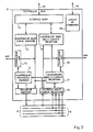
- FIG. 1 represents a computer 11, such as those on board an aerodyne. It has a redundant architecture with two processing chains each comprising a processor 35.35 'connected by a processor bus 41.41', to a memory 36.36 'containing the program executed by the processor, and to a working memory 34 , 34 ′ containing the data manipulated by the processor.
- the computer 11 also includes a bus controller 31 allowing it to communicate via at least one external bus 6, with other electronic systems on board the aerodyne.
- the computer 11 comprises an interface device 33 connected on one side to the processors 35, 35 ′ via the buses 41, 41 ′, and control signal transfer lines 42,42 ′, and the other to the bus controller 31 by means of an address and data transfer bus 39 and a control bus 40.
- a memory d exchange 32 connected to bus 39 makes it possible to store the messages received and to be sent by the external bus 6.
- the interface device 33 is, for example, integrated in an ASIC.
- the bus controller 31 is connected to two non-volatile memories 37, 38 in which are stored all the information describing the messages to be sent and received.
- these memories contain, for each data block of each message, an identification number called "label", its size and its address for storage in the exchange memory 32.
- the messages transmitted by such a bus consist of a succession of one to 31 blocks called "wordstrings", each block comprising a 20-bit label word identifying the sender of the message and the content of the block, followed by 0 to 256 words of 20-bit data.
- the identification of information associated with a label is therefore not done at the message level, but at the block level. Therefore, all of the data transfer services provided by the bus controller 31 relate to the blocks, not the messages.
- These data blocks are transmitted on a channel of the bus 6 during periodic frames, each terminal connected to the bus having the right to transmit only one periodic message during a frame, supplemented by data blocks additional aperiodics if there is free time in the frame.
- the interface device 33 is connected by three buses 41, 41 ', 39, respectively to the two processors, and to the bus controller 31, it works with three separate clocks, the first two being respectively those of the processors 35.35 ', and the third that of the bus controller 31.
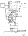
- the host interface circuit 45 makes it possible in particular to synchronize all the requests for transmission or reception of the processors 35, 35 ′. To this end, when it receives a first request from a processor, it waits with time delay for an identical request from the other processor. It then compares the first request to all requests from the other processor. If the other processor has not sent a strictly identical request to the first within a certain time, it sends an error signal to the two processors 35.35 'on the control lines 42.42' and abandons the first request . Otherwise, it activates the processing of the request.
- the controller interface circuit 48 makes it possible to develop a state of the last transmission or reception carried out by the processors 35, 35 ′. To this end, it will search in the exchange memory 32 for the control word associated with the data block transmitted or received, updated by the bus controller 31, and complete it with the result of comparisons between the signature associated with the data block in the exchange memory and the result of the calculations made by the calculation circuits 46,46 'on the data block.
- the control word managed by the bus controller 31 indicates in particular whether the data block has been refreshed since the last reading, and whether errors in the format of the data received have been detected by the bus controller 31.
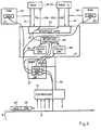
- controller 31 includes a control circuit 80 which allows an external entity to configure, monitor and control the various organs of the control unit via the control bus 40.
- the multichannel reception decoder circuit 76 is also connected to the transmission channel 7, so as to receive the data blocks transmitted by the transmission encoder circuit 71.
- the information to be transmitted used by the encoder circuit d 'transmission 71 are also supplied directly to the multi-channel reception management circuit 77, so as to allow control of the quality of the transmission by comparison of the data transmitted with that read simultaneously on the bus.
- Such a bus controller 31 can advantageously be integrated into an ASIC.
- Figures 4 to 6 illustrate the operation of the interface device 33, respectively following transmission requests, transmission control and reception, sent by the processors 35,35 '.
- the host interface circuit 45 when the host interface circuit 45 has received two strictly identical transmission requests on the control lines 42a, 42a ', coming from the two processors 35.35', it activates the circuits 49.49 'to carry out the DMA transfer of the data block 61.61' designated in the requests, working memories 34 , 34 'to the computing circuits 46,46', and from the working memory 34 of the processor 35 to the exchange memory 32 at the address indicated in the transmission requests.
- the calculation circuits 46, 46 ′ perform the signature calculation on the data to be transmitted, and the signatures thus calculated are applied to the input of the comparator 47, the signature 63 calculated by the second calculation circuit 46 ’being written in the exchange memory in association with block 61 to be transmitted.
- the information which will be transmitted on the bus will be constituted by the data block 61 produced by the processor 35 and by the signature 63 calculated by the calculation circuit 46 'from the data block 61' produced by the processor 35 '.
- the receiver will be able to detect the error , because the signature 63 will not be compatible with the data block 61.
- the comparator 47 validates the transmission by indicating the refresh by means of a refresh bit 62 in the control word 64 associated with the block to be transmitted 61 in the exchange memory 32.
- the bus controller 31 comes to consult this control word 64 at the moment when the data block must be sent on the bus, then notes that this refresh bit 62 has been set, and therefore sends the block 61 with which the signature 63 is associated on the transmission channel 7 of the bus 6.
- the controller interface circuit 48 who elaborates a word status transmitted to the processors 35,35 'by the host interface circuit 45 on the control lines 42b, 42b'.
- the bus controller 31 listens to the transmission channel 7 to receive the message that it has just transmitted, so as to make it possible to check that the transmission has taken place correctly. For this purpose, the bus controller 31 can go up in a reception area of the exchange memory 32 the data block 61 and the signature 63 which it has received, and update the control word 64 giving the result. of a certain number of low level tests carried out during the re-listening of the transmitted data block.
- the interface device 33 allows the processors 35, 35 ′ to determine the state of a transmission carried out by the bus controller 31. For this, the two processors must send to the interface device 33 a transmission control request for a specified data block.
- the host interface circuit 45 receives two identical transmission control requests originating respectively from the two processors 35, 35 ′, and insofar as the reception refresh bit 62 in the exchange memory 32 is activated, corresponding to an effective reception of the data block, it activates the DMA transfer circuits 49,49 'to transfer the data block 61 and the signature 63 received from the exchange memory 32 to the calculation circuits 46,46' which calculate the signature on the data block 61 and compare it with the associated signature 63.
- the results of the comparisons are sent to the controller interface circuit 48 which generates a transmission status word from the control word 64 read in the exchange memory 32 and from the results of the comparisons. Then, the controller interface circuit 48 sets the refresh bit 62 in the exchange memory 32 to zero, and sends the status word thus produced to the processors 35, 35 ′ on the control lines 42b, 42b 'via the host interface circuit 45.
- the host interface circuit 45 when the host interface circuit 45 receives two identical reception requests originating respectively from the two processors 35, 35 ′, and insofar as the reception refresh bit 69 of the control word 66 is activated in the exchange memory 32, corresponding to an effective reception of the data block, it activates the DMA transfer circuits 49, 49 ′ to transfer the data block 67 received from the exchange memory 32 to the working memories 34, 34 ', and the data block 67 and the signature 68 received, to the signature calculation circuits 46,46'.
- the bus controller 31 maintains a reception index in the exchange memory 32 giving the number of reception data blocks updated in the exchange memory 32.
- the two processors 35, 35 'must maintain a read index corresponding to the number of data blocks read in the exchange memory 32. The difference between these two indices gives the number of data blocks remaining to be read, with the modulo close to the size in number of blocks of the rotating buffer zone.
- the cases of overwriting of data blocks are managed by the bus controller 31 thanks to the overwrite bit contained in the control word associated with each data block in the exchange memory 32.
- the two processors 35, 35 ′ To empty a rotating buffer zone, the two processors 35, 35 ′ must send to the interface device 33 a request to read the reception index in the exchange memory 32.
- the host interface circuit 45 receives two identical requests from the two processors 35.35 ', it presents on the buses 41.41' the reception index read in the exchange memory 32.
- the processors can know whether there is at least one block of data to be read from the exchange memory 32.
- Each processor then sends a reception request associated with a read address in the exchange memory equal to the base address of the buffer zone plus the read index multiplied by the size of a block.
- the two processors 35, 35 ′ To empty all the buffer zones, the two processors 35, 35 ′ must start again reading the reception index and the reception of the data blocks stored in the exchange memory 32. These operations are for example carried out at each start of frame.
- the interface device 33 records in a stack 53 of FIFO type the signaling provided by the control unit 31 of all the labels received, possibly associating with them a date of reception. By accessing this stack 53, the processors 35, 35 ′ can thus determine which blocks are received during the last frame.
- the controller interface circuit 48 On reception of a signal by the control bus 40 indicating that the controller 31 is working in delayed reception mode, the controller interface circuit 48 is activated and recovers on the memory access bus 39 exchange 32, the access address in this memory which uniquely defines the buffer zone.
- the two processors 35,35 must send a request to read a battery 53,54, addressed to the interface device 33 which, after processing by the host interface circuit 45, presents the oldest data of a stack on the processor buses 41, 41 ′.
- These stacks 53, 54 are emptied, for example at each start of frame.
- the host interface circuit 45 also makes it possible to synchronize the two processors 35, 35 ′ with the bus controller 31, so as to minimize the difference between the instant of information generation and the instant of transmission of these by the bus controller 31.
- This mechanism makes it possible to synchronize the sequencing of the treatments with the unfolding of the frame on external bus 6.
- the bus controller 31 emits a signal at each start of frame which wakes up the controller interface circuit 48.
- the controller interface circuit 48 can then recover on the control bus 40, the address generated by the controller 31 in the non-volatile transmission memory 38, and which corresponds to the address of the descriptors of the next message to be transmitted.
- a sequencing interruption accompanied by the address of the descriptors of the message to be transmitted is then transmitted to the two processors 35, 35 ′, which should normally be waiting for this interruption. If this interruption occurs outside of a time window provided for this purpose, we are in the presence of a synchronization failure of one or of the two processors with respect to the controller 31 and a recovery processing must be carried out.
Landscapes
- Engineering & Computer Science (AREA)
- Theoretical Computer Science (AREA)
- Quality & Reliability (AREA)
- Physics & Mathematics (AREA)
- General Engineering & Computer Science (AREA)
- General Physics & Mathematics (AREA)
- Multi Processors (AREA)
- Hardware Redundancy (AREA)
Applications Claiming Priority (2)
| Application Number | Priority Date | Filing Date | Title |
|---|---|---|---|
| FR9508845A FR2737029B1 (fr) | 1995-07-19 | 1995-07-19 | Dispositif d'interface entre un calculateur a architecture redondante et un moyen de communication |
| FR9508845 | 1995-07-19 |
Publications (2)
| Publication Number | Publication Date |
|---|---|
| EP0755010A1 true EP0755010A1 (de) | 1997-01-22 |
| EP0755010B1 EP0755010B1 (de) | 2001-05-30 |
Family
ID=9481222
Family Applications (1)
| Application Number | Title | Priority Date | Filing Date |
|---|---|---|---|
| EP96401354A Expired - Lifetime EP0755010B1 (de) | 1995-07-19 | 1996-06-20 | Schnittstelleneinrichtung zwischen einem Rechner redundanter Architektur und einem Kommunikationsmittel |
Country Status (4)
| Country | Link |
|---|---|
| US (1) | US5778206A (de) |
| EP (1) | EP0755010B1 (de) |
| DE (1) | DE69613056T2 (de) |
| FR (1) | FR2737029B1 (de) |
Cited By (2)
| Publication number | Priority date | Publication date | Assignee | Title |
|---|---|---|---|---|
| FR2901379A1 (fr) * | 2006-05-19 | 2007-11-23 | Airbus France Sas | Procede et dispositif de consolidation par synchronisation logicielle dans les calculateurs des commandes de vol |
| FR2925191A1 (fr) * | 2007-12-14 | 2009-06-19 | Thales Sa | Architecture de traitement numerique a haute integrite a multiples ressources supervisees |
Families Citing this family (24)
| Publication number | Priority date | Publication date | Assignee | Title |
|---|---|---|---|---|
| US5953352A (en) * | 1997-06-23 | 1999-09-14 | Micron Electronics, Inc. | Method of checking data integrity for a raid 1 system |
| US5930484A (en) * | 1997-09-18 | 1999-07-27 | International Business Machines Corporation | Method and system for input/output control in a multiprocessor system utilizing simultaneous variable-width bus access |
| US6018780A (en) * | 1998-05-19 | 2000-01-25 | Lucent Technologies Inc. | Method and apparatus for downloading a file to a remote unit |
| DE19832060C2 (de) * | 1998-07-16 | 2000-07-06 | Siemens Ag | Doppelbare Prozessoreinrichtung |
| US6327670B1 (en) * | 1999-01-22 | 2001-12-04 | Lucent Technologies Inc. | Duplex processor with an update bus and method for operating the update bus |
| KR100324279B1 (ko) * | 1999-08-24 | 2002-02-25 | 서평원 | 교환기에서 이중화 프로세서 간 메모리 일치 시스템 및 방법 |
| FR2803057B1 (fr) * | 1999-12-22 | 2002-11-29 | Centre Nat Etd Spatiales | Systeme informatique tolerant aux erreurs transitoires et procede de gestion dans un tel systeme |
| FR2819598B1 (fr) * | 2001-01-16 | 2003-04-11 | Thomson Csf | Dispositif de synchronisation tolerant aux pannes pour reseau informatique temps reel |
| US6630872B1 (en) | 2001-07-20 | 2003-10-07 | Cmc Electronics, Inc. | Digital indirectly compensated crystal oscillator |
| FR2844946B1 (fr) * | 2002-03-15 | 2004-10-22 | Thales Sa | Procede de selection et de tri de paquets mis a disposition d'un equipement par un reseau de transmission de donnees par paquets |
| FR2840482B1 (fr) * | 2002-05-28 | 2004-10-15 | Thales Sa | Procede de reconstitution de messages achemines par un ou plusieurs reseaux de transmission par paquets |
| JP2004046455A (ja) * | 2002-07-10 | 2004-02-12 | Nec Corp | 情報処理装置 |
| US6813527B2 (en) * | 2002-11-20 | 2004-11-02 | Honeywell International Inc. | High integrity control system architecture using digital computing platforms with rapid recovery |
| US7484148B2 (en) * | 2002-12-11 | 2009-01-27 | Analog Devices, Inc. | Interface error monitor system and method |
| US20040154017A1 (en) * | 2003-01-31 | 2004-08-05 | International Business Machines Corporation | A Method and Apparatus For Dynamically Allocating Process Resources |
| DE10340236B4 (de) * | 2003-08-29 | 2006-06-01 | Infineon Technologies Ag | Anordnung mit einer Datenverarbeitungseinrichtung und einem Speicher |
| JP2006178636A (ja) * | 2004-12-21 | 2006-07-06 | Nec Corp | フォールトトレラントコンピュータ、およびその制御方法 |
| JP2006293929A (ja) * | 2005-04-14 | 2006-10-26 | Matsushita Electric Ind Co Ltd | データ伝送装置 |
| US7516246B2 (en) * | 2005-10-27 | 2009-04-07 | International Business Machines Corporation | Communications channel method for verifying integrity of untrusted subsystem responses to a request |
| US8898536B2 (en) * | 2007-04-27 | 2014-11-25 | Netapp, Inc. | Multi-core engine for detecting bit errors |
| US9158579B1 (en) | 2008-11-10 | 2015-10-13 | Netapp, Inc. | System having operation queues corresponding to operation execution time |
| US10057365B1 (en) * | 2015-06-24 | 2018-08-21 | Amazon Technologies, Inc. | Asynchronous provision of resource status data |
| US11842224B1 (en) | 2017-09-01 | 2023-12-12 | Amazon Technologies, Inc. | Synchronous and asynchronous responses to data requests from remote devices |
| DE102019106410A1 (de) * | 2019-03-13 | 2020-09-17 | Liebherr-Aerospace Lindenberg Gmbh | Vorrichtung und Verfahren zur Datenübertragung |
Citations (2)
| Publication number | Priority date | Publication date | Assignee | Title |
|---|---|---|---|---|
| DE3328405A1 (de) * | 1983-08-05 | 1985-02-21 | Siemens AG, 1000 Berlin und 8000 München | Steuerorgane eines fehlertoleranten mehrrechnersystems |
| EP0184976A2 (de) * | 1984-12-13 | 1986-06-18 | United Technologies Corporation | Interface-Vorrichtung zwischen mindestens einem Kanal und mindestens einem Bus |
Family Cites Families (6)
| Publication number | Priority date | Publication date | Assignee | Title |
|---|---|---|---|---|
| CA1179069A (en) * | 1981-04-10 | 1984-12-04 | Yasushi Fukunaga | Data transmission apparatus for a multiprocessor system |
| US4543627A (en) * | 1981-12-14 | 1985-09-24 | At&T Bell Laboratories | Internal communication arrangement for a multiprocessor system |
| EP0408810B1 (de) * | 1989-07-20 | 1996-03-20 | Kabushiki Kaisha Toshiba | Mehrprozessor-Computersystem |
| US5226152A (en) * | 1990-12-07 | 1993-07-06 | Motorola, Inc. | Functional lockstep arrangement for redundant processors |
| EP0597205B1 (de) * | 1992-09-07 | 2003-04-09 | Hitachi, Ltd. | Multiprozessorsystem und Kommunikationsverfahren zwischen Prozessoren |
| US5491787A (en) * | 1994-08-25 | 1996-02-13 | Unisys Corporation | Fault tolerant digital computer system having two processors which periodically alternate as master and slave |
-
1995
- 1995-07-19 FR FR9508845A patent/FR2737029B1/fr not_active Expired - Lifetime
-
1996
- 1996-06-20 EP EP96401354A patent/EP0755010B1/de not_active Expired - Lifetime
- 1996-06-20 DE DE69613056T patent/DE69613056T2/de not_active Expired - Lifetime
- 1996-07-19 US US08/690,156 patent/US5778206A/en not_active Expired - Lifetime
Patent Citations (2)
| Publication number | Priority date | Publication date | Assignee | Title |
|---|---|---|---|---|
| DE3328405A1 (de) * | 1983-08-05 | 1985-02-21 | Siemens AG, 1000 Berlin und 8000 München | Steuerorgane eines fehlertoleranten mehrrechnersystems |
| EP0184976A2 (de) * | 1984-12-13 | 1986-06-18 | United Technologies Corporation | Interface-Vorrichtung zwischen mindestens einem Kanal und mindestens einem Bus |
Cited By (3)
| Publication number | Priority date | Publication date | Assignee | Title |
|---|---|---|---|---|
| FR2901379A1 (fr) * | 2006-05-19 | 2007-11-23 | Airbus France Sas | Procede et dispositif de consolidation par synchronisation logicielle dans les calculateurs des commandes de vol |
| US7890221B2 (en) | 2006-05-19 | 2011-02-15 | Airbus France | Method and device for consolidation by software synchronisation in flight control computers |
| FR2925191A1 (fr) * | 2007-12-14 | 2009-06-19 | Thales Sa | Architecture de traitement numerique a haute integrite a multiples ressources supervisees |
Also Published As
| Publication number | Publication date |
|---|---|
| EP0755010B1 (de) | 2001-05-30 |
| FR2737029A1 (fr) | 1997-01-24 |
| FR2737029B1 (fr) | 1997-09-26 |
| DE69613056T2 (de) | 2002-03-21 |
| US5778206A (en) | 1998-07-07 |
| DE69613056D1 (de) | 2001-07-05 |
Similar Documents
| Publication | Publication Date | Title |
|---|---|---|
| EP0755010B1 (de) | Schnittstelleneinrichtung zwischen einem Rechner redundanter Architektur und einem Kommunikationsmittel | |
| US5170466A (en) | Storage/retrieval system for document | |
| EP0003493B1 (de) | Datenübertragungssystem zwischen Stationen die in einer Schleife miteinander verbunden sind | |
| EP0349371B1 (de) | Rechneranlage mit einer zentralen Zwischenverbindung | |
| US5321816A (en) | Local-remote apparatus with specialized image storage modules | |
| EP0860778B1 (de) | Vorrichtung und Verfahren zur Fehlererkennung in einer integrierten Schaltung mit einer parallelen-seriellen Anschlussstelle | |
| FR2508201A1 (fr) | Circuit d'interface entre un processeur et un canal de transmission | |
| EP0755013B1 (de) | Vielfachknoten-Datenverarbeitungssystem und Verfahren zur Übertragung von Nachrichten in diesem Vielfachknoten-Datenverarbeitungssystem | |
| FR2637997A1 (fr) | Procede et dispositif pour mettre en file d'attente des requetes et des reponses sur un bus | |
| FR2479534A1 (fr) | Circuit de detection d'erreur pour une memoire | |
| EP0077863A1 (de) | Abtasteinrichtung für Übertragungsleitungen, bestimmt für eine Übertragungssteuerung | |
| CA2006831C (fr) | Systeme d'emission de trames hdlc sur canal de type mic, a circuit hdlc unique et memoire tampon de transposition | |
| EP0102434A1 (de) | Anordnung zur Meldung an die zentrale Steuereinheit einer Datenverarbeitungsanlage von Fehlern, die sich in Adaptern ereignen | |
| US6366985B1 (en) | High availability asynchronous computer system | |
| EP0752669A1 (de) | Vorrichtung zur Datenübertragung zwischen einer Mehrzahl von Funktionsmodulen in einer lokalen Buseinheit und einem externen RINC-629-Bus | |
| US6912686B1 (en) | Apparatus and methods for detecting errors in data | |
| FR2765425A1 (fr) | Procede de detection d'erreurs sur une liaison serie d'un circuit integre et dispositif de mise en oeuvre du procede | |
| EP0377894B1 (de) | System zum Detektieren, dass Daten in einem Pufferspeicher gelöscht worden sind, insbesondere für einen Datenschalter | |
| US20060117076A1 (en) | Method for replication tracing | |
| EP0895159B1 (de) | Verfahren zur Entleeren von Hochdurchsatzübertragungspuffern und Vorrichtung zur Ausführung des Verfahrens | |
| FR2686991A1 (fr) | Procede, systeme et processeur de communication entre une pluralite de sous-ensembles d'un equipement. | |
| EP0974902B1 (de) | Verfahren um Fehler auf einer seriellen Verbindung einer integrierten Schaltung zu erkennen und Vorrichtung zur Durchführung des Verfahrens | |
| EP0441707B1 (de) | Koppler für Serienbus | |
| EP1426843B1 (de) | Häusliches oder industrielles lokales Netzwerk | |
| EP0636984B1 (de) | Verfahren und Vorrichtung zur Überwachung der Daten eines Rechners |
Legal Events
| Date | Code | Title | Description |
|---|---|---|---|
| PUAI | Public reference made under article 153(3) epc to a published international application that has entered the european phase |
Free format text: ORIGINAL CODE: 0009012 |
|
| 17P | Request for examination filed |
Effective date: 19960626 |
|
| AK | Designated contracting states |
Kind code of ref document: A1 Designated state(s): DE GB IT |
|
| 17Q | First examination report despatched |
Effective date: 20000204 |
|
| GRAG | Despatch of communication of intention to grant |
Free format text: ORIGINAL CODE: EPIDOS AGRA |
|
| GRAG | Despatch of communication of intention to grant |
Free format text: ORIGINAL CODE: EPIDOS AGRA |
|
| GRAH | Despatch of communication of intention to grant a patent |
Free format text: ORIGINAL CODE: EPIDOS IGRA |
|
| GRAH | Despatch of communication of intention to grant a patent |
Free format text: ORIGINAL CODE: EPIDOS IGRA |
|
| GRAA | (expected) grant |
Free format text: ORIGINAL CODE: 0009210 |
|
| AK | Designated contracting states |
Kind code of ref document: B1 Designated state(s): DE GB IT |
|
| REF | Corresponds to: |
Ref document number: 69613056 Country of ref document: DE Date of ref document: 20010705 |
|
| ITF | It: translation for a ep patent filed | ||
| GBT | Gb: translation of ep patent filed (gb section 77(6)(a)/1977) |
Effective date: 20011011 |
|
| REG | Reference to a national code |
Ref country code: GB Ref legal event code: IF02 |
|
| PLBE | No opposition filed within time limit |
Free format text: ORIGINAL CODE: 0009261 |
|
| STAA | Information on the status of an ep patent application or granted ep patent |
Free format text: STATUS: NO OPPOSITION FILED WITHIN TIME LIMIT |
|
| 26N | No opposition filed | ||
| PGFP | Annual fee paid to national office [announced via postgrant information from national office to epo] |
Ref country code: GB Payment date: 20150617 Year of fee payment: 20 Ref country code: DE Payment date: 20150616 Year of fee payment: 20 |
|
| PGFP | Annual fee paid to national office [announced via postgrant information from national office to epo] |
Ref country code: IT Payment date: 20150625 Year of fee payment: 20 |
|
| REG | Reference to a national code |
Ref country code: DE Ref legal event code: R071 Ref document number: 69613056 Country of ref document: DE |
|
| REG | Reference to a national code |
Ref country code: GB Ref legal event code: PE20 Expiry date: 20160619 |
|
| PG25 | Lapsed in a contracting state [announced via postgrant information from national office to epo] |
Ref country code: GB Free format text: LAPSE BECAUSE OF EXPIRATION OF PROTECTION Effective date: 20160619 |