EP0755010A1 - Interface device between a computer with redundant architecture and a communication means - Google Patents
Interface device between a computer with redundant architecture and a communication means Download PDFInfo
- Publication number
- EP0755010A1 EP0755010A1 EP96401354A EP96401354A EP0755010A1 EP 0755010 A1 EP0755010 A1 EP 0755010A1 EP 96401354 A EP96401354 A EP 96401354A EP 96401354 A EP96401354 A EP 96401354A EP 0755010 A1 EP0755010 A1 EP 0755010A1
- Authority
- EP
- European Patent Office
- Prior art keywords
- processors
- bus
- data
- transmitted
- controller
- Prior art date
- Legal status (The legal status is an assumption and is not a legal conclusion. Google has not performed a legal analysis and makes no representation as to the accuracy of the status listed.)
- Granted
Links
Images


Classifications
-
- G—PHYSICS
- G06—COMPUTING; CALCULATING OR COUNTING
- G06F—ELECTRIC DIGITAL DATA PROCESSING
- G06F11/00—Error detection; Error correction; Monitoring
- G06F11/07—Responding to the occurrence of a fault, e.g. fault tolerance
- G06F11/16—Error detection or correction of the data by redundancy in hardware
- G06F11/1629—Error detection by comparing the output of redundant processing systems
- G06F11/1641—Error detection by comparing the output of redundant processing systems where the comparison is not performed by the redundant processing components
-
- G—PHYSICS
- G06—COMPUTING; CALCULATING OR COUNTING
- G06F—ELECTRIC DIGITAL DATA PROCESSING
- G06F11/00—Error detection; Error correction; Monitoring
- G06F11/07—Responding to the occurrence of a fault, e.g. fault tolerance
- G06F11/16—Error detection or correction of the data by redundancy in hardware
- G06F11/1608—Error detection by comparing the output signals of redundant hardware
- G06F11/1625—Error detection by comparing the output signals of redundant hardware in communications, e.g. transmission, interfaces
-
- G—PHYSICS
- G06—COMPUTING; CALCULATING OR COUNTING
- G06F—ELECTRIC DIGITAL DATA PROCESSING
- G06F11/00—Error detection; Error correction; Monitoring
- G06F11/07—Responding to the occurrence of a fault, e.g. fault tolerance
- G06F11/16—Error detection or correction of the data by redundancy in hardware
- G06F11/1675—Temporal synchronisation or re-synchronisation of redundant processing components
- G06F11/1683—Temporal synchronisation or re-synchronisation of redundant processing components at instruction level
-
- G—PHYSICS
- G06—COMPUTING; CALCULATING OR COUNTING
- G06F—ELECTRIC DIGITAL DATA PROCESSING
- G06F2201/00—Indexing scheme relating to error detection, to error correction, and to monitoring
- G06F2201/83—Indexing scheme relating to error detection, to error correction, and to monitoring the solution involving signatures
Definitions
- the present invention relates to an interface device designed to connect a computer with redundant architecture and a communication means, such as a bus controller connected to at least one digital data transfer bus.
- computers on board aircraft which, because of the high level of reliability and security required, have a redundant architecture comprising several processors.
- Such computers are connected, via a bus control circuit, to a set of buses allowing them to communicate with the other electronic equipment of the aerodyne.
- each processor transmits messages on the bus independently of the other processors. Since all the processors run the same applications, they process the same information and therefore send the same messages on the bus to the same recipients. The recipients will therefore have to receive all the messages supposed to be identical, compare them, and reject them if they are different. These solutions therefore involve processing overload at the level of the recipients and of the bus control circuit, bus overload, and an additional cost if a control circuit and a bus are used per processor.
- the programs executed by the recipients which must include checking the messages received, will therefore depend on the hardware architecture of the transmitters. Consequently, these solutions lack flexibility by limiting the possibilities of evolution of the different computers.
- the present invention aims to eliminate these drawbacks. To this end, it offers an interface device designed to connect a computer comprising several redundant processors, to a bus controller connected to at least one digital data transfer bus,
- the interface device further comprises means for checking the integrity of each data block received by the controller, and if the received data block is integral, to validate its transfer to the memories of the respective processors.
- the interface device comprises means for calculating a signature on each block of data transmitted by each processor and received, for comparing the signatures of the blocks transmitted by each processor, for adding said signature to each block of data to be transmitted, to compare the signature calculated on each block received with that contained therein and calculated by the emitter of the block, and to develop a status word comprising the result of these comparisons and a word control signal developed and supplied by the bus controller, this status word being transmitted to all the processors.
- each processor can control the correct execution of its transmission and reception requests.
- the device according to the invention is connected to a FIFO type memory in which all the exceptions and interruptions emitted by the bus controller are stored, this memory being accessible on request sent by each processor.
- the processing carried out by the processors is not interrupted by the bus controller, the acquisition of the contexts of exceptions and interruptions taking place in a deferred and regular manner with respect to the processing. This is particularly advantageous in the case of certain critical functions which must have a deterministic temporal behavior.
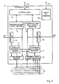
- FIG. 1 represents a computer 11, such as those on board an aerodyne. It has a redundant architecture with two processing chains each comprising a processor 35.35 'connected by a processor bus 41.41', to a memory 36.36 'containing the program executed by the processor, and to a working memory 34 , 34 ′ containing the data manipulated by the processor.
- the computer 11 also includes a bus controller 31 allowing it to communicate via at least one external bus 6, with other electronic systems on board the aerodyne.
- the computer 11 comprises an interface device 33 connected on one side to the processors 35, 35 ′ via the buses 41, 41 ′, and control signal transfer lines 42,42 ′, and the other to the bus controller 31 by means of an address and data transfer bus 39 and a control bus 40.
- a memory d exchange 32 connected to bus 39 makes it possible to store the messages received and to be sent by the external bus 6.
- the interface device 33 is, for example, integrated in an ASIC.
- the bus controller 31 is connected to two non-volatile memories 37, 38 in which are stored all the information describing the messages to be sent and received.
- these memories contain, for each data block of each message, an identification number called "label", its size and its address for storage in the exchange memory 32.
- the messages transmitted by such a bus consist of a succession of one to 31 blocks called "wordstrings", each block comprising a 20-bit label word identifying the sender of the message and the content of the block, followed by 0 to 256 words of 20-bit data.
- the identification of information associated with a label is therefore not done at the message level, but at the block level. Therefore, all of the data transfer services provided by the bus controller 31 relate to the blocks, not the messages.
- These data blocks are transmitted on a channel of the bus 6 during periodic frames, each terminal connected to the bus having the right to transmit only one periodic message during a frame, supplemented by data blocks additional aperiodics if there is free time in the frame.
- the interface device 33 is connected by three buses 41, 41 ', 39, respectively to the two processors, and to the bus controller 31, it works with three separate clocks, the first two being respectively those of the processors 35.35 ', and the third that of the bus controller 31.
- the host interface circuit 45 makes it possible in particular to synchronize all the requests for transmission or reception of the processors 35, 35 ′. To this end, when it receives a first request from a processor, it waits with time delay for an identical request from the other processor. It then compares the first request to all requests from the other processor. If the other processor has not sent a strictly identical request to the first within a certain time, it sends an error signal to the two processors 35.35 'on the control lines 42.42' and abandons the first request . Otherwise, it activates the processing of the request.
- the controller interface circuit 48 makes it possible to develop a state of the last transmission or reception carried out by the processors 35, 35 ′. To this end, it will search in the exchange memory 32 for the control word associated with the data block transmitted or received, updated by the bus controller 31, and complete it with the result of comparisons between the signature associated with the data block in the exchange memory and the result of the calculations made by the calculation circuits 46,46 'on the data block.
- the control word managed by the bus controller 31 indicates in particular whether the data block has been refreshed since the last reading, and whether errors in the format of the data received have been detected by the bus controller 31.
- controller 31 includes a control circuit 80 which allows an external entity to configure, monitor and control the various organs of the control unit via the control bus 40.
- the multichannel reception decoder circuit 76 is also connected to the transmission channel 7, so as to receive the data blocks transmitted by the transmission encoder circuit 71.
- the information to be transmitted used by the encoder circuit d 'transmission 71 are also supplied directly to the multi-channel reception management circuit 77, so as to allow control of the quality of the transmission by comparison of the data transmitted with that read simultaneously on the bus.
- Such a bus controller 31 can advantageously be integrated into an ASIC.
- Figures 4 to 6 illustrate the operation of the interface device 33, respectively following transmission requests, transmission control and reception, sent by the processors 35,35 '.
- the host interface circuit 45 when the host interface circuit 45 has received two strictly identical transmission requests on the control lines 42a, 42a ', coming from the two processors 35.35', it activates the circuits 49.49 'to carry out the DMA transfer of the data block 61.61' designated in the requests, working memories 34 , 34 'to the computing circuits 46,46', and from the working memory 34 of the processor 35 to the exchange memory 32 at the address indicated in the transmission requests.
- the calculation circuits 46, 46 ′ perform the signature calculation on the data to be transmitted, and the signatures thus calculated are applied to the input of the comparator 47, the signature 63 calculated by the second calculation circuit 46 ’being written in the exchange memory in association with block 61 to be transmitted.
- the information which will be transmitted on the bus will be constituted by the data block 61 produced by the processor 35 and by the signature 63 calculated by the calculation circuit 46 'from the data block 61' produced by the processor 35 '.
- the receiver will be able to detect the error , because the signature 63 will not be compatible with the data block 61.
- the comparator 47 validates the transmission by indicating the refresh by means of a refresh bit 62 in the control word 64 associated with the block to be transmitted 61 in the exchange memory 32.
- the bus controller 31 comes to consult this control word 64 at the moment when the data block must be sent on the bus, then notes that this refresh bit 62 has been set, and therefore sends the block 61 with which the signature 63 is associated on the transmission channel 7 of the bus 6.
- the controller interface circuit 48 who elaborates a word status transmitted to the processors 35,35 'by the host interface circuit 45 on the control lines 42b, 42b'.
- the bus controller 31 listens to the transmission channel 7 to receive the message that it has just transmitted, so as to make it possible to check that the transmission has taken place correctly. For this purpose, the bus controller 31 can go up in a reception area of the exchange memory 32 the data block 61 and the signature 63 which it has received, and update the control word 64 giving the result. of a certain number of low level tests carried out during the re-listening of the transmitted data block.
- the interface device 33 allows the processors 35, 35 ′ to determine the state of a transmission carried out by the bus controller 31. For this, the two processors must send to the interface device 33 a transmission control request for a specified data block.
- the host interface circuit 45 receives two identical transmission control requests originating respectively from the two processors 35, 35 ′, and insofar as the reception refresh bit 62 in the exchange memory 32 is activated, corresponding to an effective reception of the data block, it activates the DMA transfer circuits 49,49 'to transfer the data block 61 and the signature 63 received from the exchange memory 32 to the calculation circuits 46,46' which calculate the signature on the data block 61 and compare it with the associated signature 63.
- the results of the comparisons are sent to the controller interface circuit 48 which generates a transmission status word from the control word 64 read in the exchange memory 32 and from the results of the comparisons. Then, the controller interface circuit 48 sets the refresh bit 62 in the exchange memory 32 to zero, and sends the status word thus produced to the processors 35, 35 ′ on the control lines 42b, 42b 'via the host interface circuit 45.
- the host interface circuit 45 when the host interface circuit 45 receives two identical reception requests originating respectively from the two processors 35, 35 ′, and insofar as the reception refresh bit 69 of the control word 66 is activated in the exchange memory 32, corresponding to an effective reception of the data block, it activates the DMA transfer circuits 49, 49 ′ to transfer the data block 67 received from the exchange memory 32 to the working memories 34, 34 ', and the data block 67 and the signature 68 received, to the signature calculation circuits 46,46'.
- the bus controller 31 maintains a reception index in the exchange memory 32 giving the number of reception data blocks updated in the exchange memory 32.
- the two processors 35, 35 'must maintain a read index corresponding to the number of data blocks read in the exchange memory 32. The difference between these two indices gives the number of data blocks remaining to be read, with the modulo close to the size in number of blocks of the rotating buffer zone.
- the cases of overwriting of data blocks are managed by the bus controller 31 thanks to the overwrite bit contained in the control word associated with each data block in the exchange memory 32.
- the two processors 35, 35 ′ To empty a rotating buffer zone, the two processors 35, 35 ′ must send to the interface device 33 a request to read the reception index in the exchange memory 32.
- the host interface circuit 45 receives two identical requests from the two processors 35.35 ', it presents on the buses 41.41' the reception index read in the exchange memory 32.
- the processors can know whether there is at least one block of data to be read from the exchange memory 32.
- Each processor then sends a reception request associated with a read address in the exchange memory equal to the base address of the buffer zone plus the read index multiplied by the size of a block.
- the two processors 35, 35 ′ To empty all the buffer zones, the two processors 35, 35 ′ must start again reading the reception index and the reception of the data blocks stored in the exchange memory 32. These operations are for example carried out at each start of frame.
- the interface device 33 records in a stack 53 of FIFO type the signaling provided by the control unit 31 of all the labels received, possibly associating with them a date of reception. By accessing this stack 53, the processors 35, 35 ′ can thus determine which blocks are received during the last frame.
- the controller interface circuit 48 On reception of a signal by the control bus 40 indicating that the controller 31 is working in delayed reception mode, the controller interface circuit 48 is activated and recovers on the memory access bus 39 exchange 32, the access address in this memory which uniquely defines the buffer zone.
- the two processors 35,35 must send a request to read a battery 53,54, addressed to the interface device 33 which, after processing by the host interface circuit 45, presents the oldest data of a stack on the processor buses 41, 41 ′.
- These stacks 53, 54 are emptied, for example at each start of frame.
- the host interface circuit 45 also makes it possible to synchronize the two processors 35, 35 ′ with the bus controller 31, so as to minimize the difference between the instant of information generation and the instant of transmission of these by the bus controller 31.
- This mechanism makes it possible to synchronize the sequencing of the treatments with the unfolding of the frame on external bus 6.
- the bus controller 31 emits a signal at each start of frame which wakes up the controller interface circuit 48.
- the controller interface circuit 48 can then recover on the control bus 40, the address generated by the controller 31 in the non-volatile transmission memory 38, and which corresponds to the address of the descriptors of the next message to be transmitted.
- a sequencing interruption accompanied by the address of the descriptors of the message to be transmitted is then transmitted to the two processors 35, 35 ′, which should normally be waiting for this interruption. If this interruption occurs outside of a time window provided for this purpose, we are in the presence of a synchronization failure of one or of the two processors with respect to the controller 31 and a recovery processing must be carried out.
Abstract
Description
La présente invention concerne un dispositif d'interface conçu pour connecter un calculateur à architecture redondante et un moyen de communication, tel qu'un contrôleur de bus connecté à au moins un bus de transfert de données numériques.The present invention relates to an interface device designed to connect a computer with redundant architecture and a communication means, such as a bus controller connected to at least one digital data transfer bus.
Elle s'applique notamment, mais non exclusivement, aux calculateurs embarqués à bords des aérodynes, qui en raison du haut niveau de fiabilité et de sécurité requis, présentent une architecture redondante comportant plusieurs processeurs. De tels calculateurs sont raccordés, par l'intermédiaire d'un circuit de contrôle de bus, à un ensemble de bus leur permettant de communiquer avec les autres équipements électroniques de l'aérodyne.It applies in particular, but not exclusively, to computers on board aircraft, which, because of the high level of reliability and security required, have a redundant architecture comprising several processors. Such computers are connected, via a bus control circuit, to a set of buses allowing them to communicate with the other electronic equipment of the aerodyne.
Dans ce type d'application, il se pose le problème du raccordement des sorties des processeurs du calculateur au circuit de contrôle de bus. Ce problème peut être résolu par deux types de solutions.In this type of application, there is the problem of connecting the outputs of the processors of the computer to the bus control circuit. This problem can be solved by two types of solutions.
Dans les solutions du premier type, chaque processeur émet des messages sur le bus d'une manière indépendante des autres processeurs. Etant donné que tous les processeurs exécutent les mêmes applications, ils élaborent les mêmes informations et donc émettent les mêmes messages sur le bus vers les mêmes destinataires. Les destinataires devront donc effectuer la réception de tous les messages sensés être identiques, les comparer, et les rejeter s'ils sont différents. Ces solutions impliquent donc une surcharge de traitement au niveau des destinataires et du circuit de contrôle de bus, une surcharge du bus, et un coût supplémentaire si l'on met en oeuvre un circuit de contrôle et un bus par processeur.
En outre, les programmes exécutés par les destinataires qui doivent inclure le contrôle des messages reçus, vont donc dépendre de l'architecture matérielle des émetteurs. Par conséquent, ces solutions manquent de souplesse en limitant les possibilités d'évolution des différents calculateurs.In solutions of the first type, each processor transmits messages on the bus independently of the other processors. Since all the processors run the same applications, they process the same information and therefore send the same messages on the bus to the same recipients. The recipients will therefore have to receive all the messages supposed to be identical, compare them, and reject them if they are different. These solutions therefore involve processing overload at the level of the recipients and of the bus control circuit, bus overload, and an additional cost if a control circuit and a bus are used per processor.
In addition, the programs executed by the recipients, which must include checking the messages received, will therefore depend on the hardware architecture of the transmitters. Consequently, these solutions lack flexibility by limiting the possibilities of evolution of the different computers.
Dans les solutions du second type, à deux processeurs redondants, les informations en sortie des processeurs du calculateur sont comparées, un seul message étant émis sur le bus lorsque les informations fournies par les processeurs sont identiques. Cette opération de comparaison est généralement effectuée par chaque processeur, mais un seul processeur a accès en émission au circuit de contrôle de bus, tandis que l'autre processeur a en général moyen d'invalider le circuit de contrôle de bus en cas de détection d'une divergence, ou peut indiquer aux destinataires par un moyen parallèle que les informations émises sur le bus sont invalides.
Ces solutions impliquent donc une surcharge de traitement au niveau des processeurs des émetteurs. Par ailleurs, étant donné que seul un processeur à accès en émission au circuit de contrôle, les programmes exécutés par les processeurs d'un même calculateur sont différents, ce qui entraîne un coût supplémentaire.In solutions of the second type, with two redundant processors, the information output from the computer processors is compared, a single message being sent on the bus when the information provided by the processors is identical. This comparison operation is generally carried out by each processor, but only one processor has transmission access to the bus control circuit, while the other processor generally has the means of invalidating the bus control circuit in the event of detection of '' a discrepancy, or may indicate to the recipients by a parallel means that the information transmitted on the bus is invalid.
These solutions therefore involve processing overload at the level of the processors of the transmitters. Furthermore, since only one processor has transmission access to the control circuit, the programs executed by the processors of the same computer are different, which involves an additional cost.
La présente invention a pour but de supprimer ces inconvénients. A cet effet, elle propose un dispositif d'interface conçu pour connecter un calculateur comprenant plusieurs processeurs redondants, à un contrôleur de bus relié à au moins un bus de transfert de données numériques,The present invention aims to eliminate these drawbacks. To this end, it offers an interface device designed to connect a computer comprising several redundant processors, to a bus controller connected to at least one digital data transfer bus,
Le dispositif d'interface est caractérisé en ce qu'il comprend :
- des moyens pour synchroniser et comparer les requêtes d'émission et de réception de blocs de données émises respectivement par les processeurs, et pour déclencher le traitement d'une requête lorsque celle-ci a été émise par tous les processeurs,
- des moyens pour transférer les blocs de données à émettre ou reçus par le contrôleur de bus, entre le contrôleur de bus et les mémoires de travail respectives des processeurs, et
- des moyens pour comparer les blocs de données à émettre fournis respectivement par les processeurs et, pour déclencher le transfert d'un bloc de données s'il se trouve d'une manière identique en sortie de tous les processeurs, de la mémoire de travail d'un des processeurs vers le contrôleur de bus, en vue de son émission sur le bus.
- means for synchronizing and comparing the requests for sending and receiving blocks of data sent respectively by the processors, and for triggering the processing of a request when the latter has been sent by all the processors,
- means for transferring the data blocks to be sent or received by the bus controller, between the bus controller and the respective working memories of the processors, and
- means for comparing the data blocks to be transmitted supplied respectively by the processors and, for triggering the transfer of a data block if it is found in an identical manner at the output of all the processors, from the working memory d 'one of the processors to the bus controller, with a view to its transmission on the bus.
De cette manière, on a regroupé dans un dispositif distinct des processeurs de traitement, toutes les tâches de synchronisation des processeurs, de transfert de données entre les processeurs et le contrôleur de bus, et de contrôle d'intégrité, qui doivent être effectuées à chaque émission et réception de données par un ensemble de processeurs redondants. De ce fait, les processeurs du calculateur se trouvent complètement déchargés de ces tâches et les programmes exécutés par les processeurs peuvent ainsi être identiques et indépendants de l'architecture du calculateur, et la gestion de la redondance devient transparente au niveau des programmes.
D'autre part, le dispositif d'interface évite d'avoir à réaliser un couplage matériel très strict (cycle par cycle des processeurs) entre les processeurs de traitement.In this way, all of the processor synchronization tasks, data transfer between the processors and the bus controller, and integrity check, which must be performed each time, have been grouped together in a separate device for the processing processors. transmission and reception of data by a set of redundant processors. As a result, the processors of the computer are completely relieved of these tasks and the programs executed by the processors can thus be identical and independent of the architecture of the computer, and the management of redundancy becomes transparent at the program level.
On the other hand, the interface device avoids having to carry out a very strict hardware coupling (cycle by cycle of the processors) between the processing processors.
Selon une particularité de l'invention, le dispositif d'interface comprend en outre des moyens pour contrôler l'intégrité de chaque bloc de données reçu par le contrôleur, et si le bloc de données reçu est intègre, pour valider son transfert vers les mémoires de travail respectives des processeurs.According to a feature of the invention, the interface device further comprises means for checking the integrity of each data block received by the controller, and if the received data block is integral, to validate its transfer to the memories of the respective processors.
Grâce à cette disposition, les processeurs sont également déchargés du contrôle d'intégrité des informations reçues.Thanks to this arrangement, the processors are also relieved of the integrity check of the information received.
Selon une autre particularité de l'invention, le dispositif d'interface comprend des moyens pour calculer une signature sur chaque bloc de données émis par chaque processeur et reçu, pour comparer entre elles les signatures des blocs émis par chaque processeur, pour ajouter ladite signature à chaque bloc de données à émettre, pour comparer la signature calculée sur chaque bloc reçu avec celle contenue dans celui-ci et calculée par l'émetteur du bloc, et pour élaborer un mot d'état comprenant le résultat de ces comparaisons et un mot de contrôle élaboré et fourni par le contrôleur de bus, ce mot d'état étant transmis à tous les processeurs.According to another feature of the invention, the interface device comprises means for calculating a signature on each block of data transmitted by each processor and received, for comparing the signatures of the blocks transmitted by each processor, for adding said signature to each block of data to be transmitted, to compare the signature calculated on each block received with that contained therein and calculated by the emitter of the block, and to develop a status word comprising the result of these comparisons and a word control signal developed and supplied by the bus controller, this status word being transmitted to all the processors.
Ainsi chaque processeur peut contrôler la bonne exécution de ses requêtes d'émission et de réception.Thus each processor can control the correct execution of its transmission and reception requests.
Avantageusement, le dispositif selon l'invention est connecté à une mémoire de type FIFO dans laquelle sont stockées toutes les exceptions et interruptions émises par le contrôleur de bus, cette mémoire étant accessible sur requête émise par chaque processeur.Advantageously, the device according to the invention is connected to a FIFO type memory in which all the exceptions and interruptions emitted by the bus controller are stored, this memory being accessible on request sent by each processor.
De cette manière, les traitements effectués par les processeurs ne sont pas interrompus par le contrôleur de bus, l'acquisition des contextes d'exceptions et d'interruptions s'effectuant de manière différée et régulière par rapport aux traitements. Ceci est particulièrement avantageux dans le cas de certaines fonctions critiques qui doivent avoir un comportement temporel déterministe.In this way, the processing carried out by the processors is not interrupted by the bus controller, the acquisition of the contexts of exceptions and interruptions taking place in a deferred and regular manner with respect to the processing. This is particularly advantageous in the case of certain critical functions which must have a deterministic temporal behavior.
Un mode de réalisation du dispositif selon l'invention sera décrit ci-après, à titre d'exemple non limitatif, avec référence aux dessins annexés dans lesquels :
- La figure 1 représente schématiquement un calculateur à deux processeurs redondants utilisant le dispositif d'interface selon l'invention ;
- La figure 2 est un schéma bloc du dispositif d'interface ;
- La figure 3 illustre un mode de réalisation d'un contrôleur de bus ;
- Les figures 4 à 6 illustrent le fonctionnement du dispositif d'interface.
- FIG. 1 schematically represents a computer with two redundant processors using the interface device according to the invention;
- Figure 2 is a block diagram of the interface device;
- FIG. 3 illustrates an embodiment of a bus controller;
- Figures 4 to 6 illustrate the operation of the interface device.
La figure 1 représente un calculateur 11, tel que ceux embarqués à bord d'un aérodyne. Il présente une architecture redondante à deux chaînes de traitement comprenant chacune un processeur 35,35' connecté par un bus processeur 41,41', à une mémoire 36,36' contenant le programme exécuté par le processeur, et à une mémoire de travail 34,34' contenant les données manipulées par le processeur.FIG. 1 represents a
Le calculateur 11 comprend également un contrôleur de bus 31 lui permettant de communiquer par l'intermédiaire d'au moins un bus externe 6, avec d'autres systèmes électroniques embarqués à bord de l'aérodyne.The
Par ailleurs, afin d'établir la connexion des deux chaînes de traitement avec un contrôleur de bus commun, le calculateur 11 comprend un dispositif d'interface 33 connecté d'un côté aux processeurs 35,35' par l'intermédiaire des bus 41,41', et de lignes de transfert de signaux de contrôle 42,42', et de l'autre au contrôleur de bus 31 grâce à un bus 39 de transfert d'adresses et de données et un bus de contrôle 40. Une mémoire d'échange 32 raccordée au bus 39 permet de stocker les messages reçus et à émettre par le bus externe 6. Le dispositif d'interface 33 est, par exemple, intégré dans un ASIC.Furthermore, in order to establish the connection of the two processing chains with a common bus controller, the
Dans le cas d'un bus externe 6 de type ARINC 629, le contrôleur de bus 31 est connecté à deux mémoires non volatiles 37,38 dans lesquelles sont mémorisées toutes les informations décrivant les messages à émettre et à recevoir. En particulier, ces mémoires contiennent pour chaque bloc de données de chaque message, un numéro d'identification appelé "label", sa taille et son adresse de rangement dans la mémoire d'échange 32.In the case of an
Selon la norme ARINC 629, les messages transmis par un tel bus sont constitués par une succession de un à 31 blocs appelés "wordstrings", chaque bloc comprenant un mot de label sur 20 bits identifiant l'émetteur du message et le contenu du bloc, suivi de 0 à 256 mots de données sur 20 bits. Le repérage des informations associées à un label ne se fait donc pas au niveau des messages, mais au niveau des blocs. Par conséquent, tous les services de transfert de données fournis par le contrôleur de bus 31 portent sur les blocs, et non pas sur les messages.
Ces blocs de données sont émis sur un canal du bus 6 au cours de trames périodiques, chaque terminal connecté au bus n'ayant le droit d'émettre qu'un seul message périodique au cours d'une trame, complété par des blocs de données apériodiques supplémentaires s'il reste du temps libre dans la trame.According to the ARINC 629 standard, the messages transmitted by such a bus consist of a succession of one to 31 blocks called "wordstrings", each block comprising a 20-bit label word identifying the sender of the message and the content of the block, followed by 0 to 256 words of 20-bit data. The identification of information associated with a label is therefore not done at the message level, but at the block level. Therefore, all of the data transfer services provided by the
These data blocks are transmitted on a channel of the
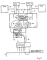
Tel que représenté sur la figure 2, le dispositif d'interface 33 selon l'invention comprend :
- un circuit d'interface
hôte 45 connecté à la fois aux lignes decontrôle 42,42' et auxbus 41,41' des deuxprocesseurs 35,35', et assurant la synchronisation des requêtes émises par les deuxprocesseurs 35,35' et la transmission aux processeurs de mots d'état de compte-rendu d'émission et de réception, - deux
circuits 46,46' de calcul de signature (par exemple de type somme de contrôle ou CRC : "Cyclic Redundancy Check") sur le contenu des blocs de données à émettre ou reçus par le contrôleur debus 31, ces circuits de calcul étant affectés respectivement aux deux processeurs, - un
comparateur 47 permettant de vérifier l'égalité des signatures élaborées par les deux circuits decalcul 46,46', et ainsi de vérifier la cohérence des blocs émis respectivement par les deuxprocesseurs 35,35', - un circuit d'interface
contrôleur 48 réalisant notamment l'élaboration d'un mot d'état de la dernière émission ou réception effectuée par le contrôleur de bus, et - deux circuits de transfert DMA (Direct Memory Access) 49,49' permettant d'effectuer des transferts de données de mémoire à mémoire entre les mémoires de
travail 34,34' des deuxprocesseurs 35,35' et la mémoire d'échange 32.
- a
host interface circuit 45 connected both to thecontrol lines 42,42 'and to thebuses 41,41' of the twoprocessors 35,35 ', and ensuring the synchronization of the requests sent by the twoprocessors 35,35' and the transmission to the processors of transmission and reception report status words, - two
signature calculation circuits bus controller 31, these calculation circuits being assigned respectively to the two processors, - a
comparator 47 making it possible to check the equality of the signatures produced by the twocalculation circuits 46,46 ', and thus to check the consistency of the blocks emitted respectively by the twoprocessors 35,35', - a
controller interface circuit 48 carrying out in particular the preparation of a status word of the last transmission or reception carried out by the bus controller, and - two transfer circuits DMA (Direct Memory Access) 49.49 'allowing data transfers from memory to memory between the working memories 34.34' of the two processors 35.35 'and the
exchange memory 32.
Par ailleurs, étant donné que le dispositif d'interface 33 est connecté par trois bus 41,41',39, respectivement aux deux processeurs, et au contrôleur de bus 31, il travaille avec trois horloges distinctes, les deux premières étant respectivement celles des processeurs 35,35', et la troisième celle du contrôleur de bus 31.Furthermore, since the
Le circuit d'interface hôte 45 permet notamment de synchroniser toutes les requêtes d'émission ou de réception des processeurs 35,35'. A cet effet, lorsqu'il reçoit une première requête d'un processeur, il se met en attente avec temporisation d'une requête identique en provenance de l'autre processeur. Il compare ensuite la première requête à toutes les requêtes émises par l'autre processeur. Si l'autre processeur n'a pas émis une requête strictement identique à la première dans un certain délai, il envoie un signal d'erreur aux deux processeurs 35,35' sur les lignes de contrôle 42,42' et abandonne la première requête. Dans le cas contraire, il active le traitement de la requête.The
Le circuit d'interface contrôleur 48 permet d'élaborer un état de la dernière émission ou réception effectuée par les processeurs 35,35'. A cet effet, il va rechercher dans la mémoire d'échange 32 le mot de contrôle associé au bloc de données émis ou reçu, mis à jour par le contrôleur de bus 31, et le complète avec le résultat des comparaisons entre la signature associée au bloc de données dans la mémoire d'échange et le résultat des calculs effectués par les circuits de calcul 46,46' sur le bloc de données.The
Le mot de contrôle géré par le contrôleur de bus 31 indique notamment si le bloc de données a été rafraîchi depuis la dernière lecture, et si des erreurs sur le format des données reçues ont été détectées par le contrôleur de bus 31.The control word managed by the
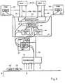
La figure 3 montre un exemple d'architecture fonctionnelle du contrôleur de bus 31, relié à un bus externe 6 comportant par exemple, un canal d'émission 7 et une pluralité de canaux de réception 8, chacun de ces canaux étant de type ARINC 629. UN tel contrôleur de bus comprend, pour l'émission de message sur le canal 7 du bus externe 6 :
- un
circuit encodeur d'émission 71 connectéau canal d'émission 7, ce circuit réalisant le formatage, la sérialisation et l'encodage des informations à émettre, - un circuit de contrôle de protocole d'émission 72 qui réalise la gestion du protocole (format temporel) de prise de décision d'émission des informations sur le bus, et le pilotage du format spatial des messages en émission,
- un circuit de contrôle 73 de la mémoire non
volatile d'émission 38 contenant la description des messages à émettre, et l'adresse de ces derniers dans la mémoire d'échange 32, ce circuit de contrôle 73 effectuant la lecture des informations décrivant chaque bloc de données d'un message à émettre donné, contenues dans la mémoire nonvolatile XPP 38, et - un circuit de contrôle en émission 74 de la mémoire d'échange 32, qui réalise la gestion en émission d'un
circuit d'interface 75 pour l'acquisition et la surveillance des informations à émettre,le circuit d'interface 75 effectuant la gestion des différentes demandes d'accès à la mémoire d'échange 32 viale bus 39.
- a
transmission encoder circuit 71 connected to thetransmission channel 7, this circuit performing the formatting, serialization and encoding of the information to be transmitted, - a transmission
protocol control circuit 72 which manages the protocol (time format) for making decision to transmit information on the bus, and driving the spatial format of the messages in transmission, - a
control circuit 73 of thenon-volatile transmission memory 38 containing the description of the messages to be transmitted, and the address of the latter in theexchange memory 32, thiscontrol circuit 73 reading the information describing each block data of a given message to be transmitted, contained in thenon-volatile memory XPP 38, and - a
transmission control circuit 74 of theexchange memory 32, which performs transmission management of aninterface circuit 75 for the acquisition and monitoring of the information to be transmitted, theinterface circuit 75 performing the management different requests for access to theexchange memory 32 via thebus 39.
Le contrôleur 31 comprend, pour la réception des informations transitant sur les canaux de réception 8 du bus 6 :
- un circuit décodeur de réception multicanaux 76 conçu pour détecter l'activité de chaque canal, désérialiser les informations reçues sur chacun des canaux 8, et effectuer des surveillances de niveau physique et partiellement logique canal par canal,
- un circuit de gestion de réception multicanaux 77 qui effectue la gestion et la surveillance des mots de label et de donnée reçus sur chaque canal, ainsi que l'ordonnancement des traitements à effectuer pour la réception des informations transmises par chaque canal,
- un circuit de contrôle 78 de la mémoire non volatile de réception 37 contenant la description des blocs de données à recevoir, et l'adresse de ces derniers dans la mémoire d'échange 32, ce circuit de contrôle 78 effectuant la lecture des informations décrivant un bloc de données reçu par un canal, contenues dans la mémoire non volatile de réception 37, et
- un circuit de contrôle de réception 79 de la mémoire d'échange 32 qui réalise la gestion en réception du
circuit d'interface 75 pour la fourniture et la surveillance des informations reçues.
- a multi-channel
reception decoder circuit 76 designed to detect the activity of each channel, deserialize the information received on each of thechannels 8, and perform physical and partially logical level monitoring channel by channel, - a multi-channel
reception management circuit 77 which performs the management and monitoring of the label and data words received on each channel, as well as the scheduling of the processing operations to be carried out for the reception of the information transmitted by each channel, - a
control circuit 78 of thenon-volatile reception memory 37 containing the description of the data blocks to be received, and the address of the latter in theexchange memory 32, thiscontrol circuit 78 reading the information describing a block of data received by a channel, contained in thenon-volatile reception memory 37, and - a
reception control circuit 79 of theexchange memory 32 which performs reception management of theinterface circuit 75 for the supply and monitoring of the information received.
Par ailleurs, le contrôleur 31 comprend un circuit de commande 80 qui permet à une entité externe de configurer, surveiller et commander les différents organes de l'unité de contrôle par l'intermédiaire du bus de contrôle 40.Furthermore, the
Il convient de noter que le circuit décodeur de réception multicanaux 76 est également connecté au canal d'émission 7, de manière à recevoir les blocs de données émis par le circuit encodeur d'émission 71. Les informations à émettre utilisées par le circuit encodeur d'émission 71 sont également fournies directement au circuit de gestion de réception multi-canaux 77, de manière à permettre le contrôle de la qualité de l'émission par comparaison des données émises avec celles lues simultanément sur le bus.It should be noted that the multichannel
Un tel contrôleur de bus 31 peut avantageusement être intégré dans un ASIC.Such a
Les figures 4 à 6 illustrent le fonctionnement du dispositif d'interface 33, respectivement à la suite de requêtes d'émission, de contrôle d'émission et de réception, émises par les processeurs 35,35'.Figures 4 to 6 illustrate the operation of the
Sur la figure 4, lorsque le circuit d'interface hôte 45 a reçu deux requêtes d'émission strictement identiques sur les lignes de contrôle 42a,42a', en provenance des deux processeurs 35,35', il active les circuits 49,49' pour effectuer le transfert DMA du bloc de données 61,61' désigné dans les requêtes, des mémoires de travail 34,34' vers le circuits de calcul 46,46', et de la mémoire de travail 34 du processeur 35 vers la mémoire d'échange 32 à l'adresse indiquée dans les requêtes d'émission. Parallèlement, les circuits de calcul 46,46' effectuent le calcul de signature sur les données à émettre, et les signatures ainsi calculées sont appliquées à l'entrée du comparateur 47, la signature 63 calculée par le second circuit de calcul 46' étant inscrite dans la mémoire d'échange en association avec le bloc 61 à transmettre.In FIG. 4, when the
Ainsi, l'information qui sera émise sur le bus sera constituée par le bloc de données 61 élaboré par le processeur 35 et par la signature 63 calculée par le circuit de calcul 46' à partir du bloc de données 61' élaborée par le processeur 35'. Ainsi, même en cas de panne du comparateur 47, élément unique qui alors ne détecterait pas une divergence entre les données émises par les processeurs 35,35', et laisserait donc partir un bloc de données non valide, le récepteur pourra détecter l'erreur, car la signature 63 ne sera pas compatible avec le bloc de données 61.Thus, the information which will be transmitted on the bus will be constituted by the data block 61 produced by the
Si les signatures calculées par les deux circuits 46,46' sont identiques, le comparateur 47 valide l'émission en indiquant le rafraîchissement par l'intermédiaire d'un bit de rafraîchissement 62 dans le mot de contrôle 64 associé au bloc à transmettre 61 dans la mémoire d'échange 32. Le contrôleur de bus 31 vient consulter ce mot de contrôle 64 au moment où le bloc de données devra être émis sur le bus, constate alors que ce bit de rafraîchissement 62 a été positionné, et donc émet le bloc de données 61 auquel est associé la signature 63 sur le canal d'émission 7 du bus 6. Par contre, si les signatures calculées par les deux circuits 46,46' sont différentes, l'erreur est consignée par le circuit d'interface contrôleur 48 qui élabore un mot d'état transmis aux processeurs 35,35' par le circuit d'interface hôte 45 sur les lignes de contrôle 42b,42b'.If the signatures calculated by the two
Selon la norme ARINC 629, le contrôleur de bus 31 est à l'écoute du canal d'émission 7 pour recevoir le message qu'il vient d'émettre, de manière à permettre de contrôler que l'émission s'est correctement déroulée. A cet effet, le contrôleur de bus 31 peut remonter dans une zone de réception de la mémoire d'échange 32 le bloc de données 61 et la signature 63 qu'il a reçus, et mettre à jour le mot de contrôle 64 donnant le résultat d'un certain nombre de tests de bas niveau effectués lors de la ré-écoute du bloc de données émis.According to the ARINC 629 standard, the
Comme l'illustre la figure 5, le dispositif d'interface 33 permet aux processeurs 35,35' de déterminer l'état d'une émission effectuée par le contrôleur de bus 31.
Pour cela, les deux processeurs doivent envoyer au dispositif d'interface 33 une requête de contrôle d'émission pour un bloc de données indiqué. Lorsque le circuit d'interface hôte 45 reçoit deux requêtes de contrôle d'émission identiques en provenance respectivement des deux processeurs 35,35', et dans la mesure où le bit de rafraîchissement en réception 62 dans la mémoire d'échange 32 est activé, correspondant à une réception effective du bloc de données, il active les circuits de transfert DMA 49,49' pour transférer le bloc de données 61 et la signature 63 reçus de la mémoire d'échange 32 vers les circuits de calcul 46,46' qui calculent la signature sur le bloc de données 61 et la comparent avec la signature 63 associée. Les résultats des comparaisons sont envoyés au circuit d'interface contrôleur 48 qui élabore un mot d'état d'émission à partir du mot de contrôle 64 lu dans la mémoire d'échange 32 et des résultats des comparaisons. Ensuite, le circuit d'interface contrôleur 48 met à zéro le bit de rafraîchissement 62 dans la mémoire d'échange 32, et envoie le mot d'état ainsi élaboré aux processeurs 35,35' sur les lignes de contrôle 42b,42b' par l'intermédiaire du circuit d'interface hôte 45.As illustrated in FIG. 5, the
For this, the two processors must send to the interface device 33 a transmission control request for a specified data block. When the
Sur la figure 6, lorsque le circuit d'interface hôte 45 reçoit deux requêtes de réception identiques en provenance respectivement des deux processeurs 35,35', et dans la mesure où le bit de rafraîchissement en réception 69 du mot de contrôle 66 est activé dans la mémoire d'échange 32, correspondant à une réception effective du bloc de données, il active les circuits de transfert DMA 49,49' pour transférer le bloc de données 67 reçu de la mémoire d'échange 32 vers les mémoires de travail 34,34', et le bloc de données 67 et la signature 68 reçue, vers les circuits de calcul de signature 46,46'. Ces deux circuits effectuent alors le calcul de la signature sur le bloc de données 67, comparent le résultat obtenu à la signature reçue 68, et transmettent le résultat de la comparaison au circuit d'interface contrôleur 48 qui va lire dans la mémoire d'échange 32, le mot de contrôle 66 associé au bloc de donnée reçu 67. Ensuite, le circuit d'interface contrôleur 48 élabore un mot d'état de réception regroupant le mot de contrôle 66 et les résultats des comparaisons, qui est transmis au circuit d'interface hôte 45, et désactive le bit de rafraîchissement 69 dans la mémoire d'échange 32.In FIG. 6, when the
Pour ne pas avoir à interrompre les applications exécutées par les processeurs 35,35', on a prévu un mode de réception différé dans lequel les zones de mémorisation des blocs de données reçus sont gérées en zone tampon tournante, permettant ainsi de différer la lecture des données par les processeurs 35,35', sans risque d'écrasement des données.In order not to have to interrupt the applications executed by the
En réception différée, le contrôleur de bus 31 tient à jour un indice de réception dans la mémoire d'échange 32 donnant le nombre de blocs de données en réception mis à jour dans la mémoire d'échange 32. Parallèlement, les deux processeurs 35,35' doivent tenir à jour un indice de lecture correspondant au nombre de blocs de données lus dans la mémoire d'échange 32. La différence entre ces deux indices donne le nombre de blocs de données restant à lire, au modulo près de la taille en nombre de blocs de la zone tampon tournante. Par ailleurs, les cas d'écrasement de blocs de données sont gérés par le contrôleur de bus 31 grâce au bit d'écrasement contenu dans le mot de contrôle associé à chaque bloc de données dans la mémoire d'échange 32.In delayed reception, the
Pour vider une zone tampon tournante, les deux processeurs 35,35' doivent envoyer au dispositif d'interface 33 une requête de lecture de l'indice de réception dans la mémoire d'échange 32. Lorsque le circuit d'interface hôte 45 reçoit deux requêtes identiques des deux processeurs 35,35', il présente sur les bus 41,41' l'indice de réception lu dans la mémoire d'échange 32. En fonction de l'écart entre les indices gérés par les processeurs 35,35' et l'indice lu dans la mémoire d'échange 32, les processeurs peuvent savoir s'il y a au moins un bloc de données à lire dans la mémoire d'échange 32.
Chaque processeur émet alors une requête de réception associée à une adresse de lecture dans la mémoire d'échange égale à l'adresse de base de la zone tampon additionnée de l'indice de lecture multiplié par la taille d'un bloc. Pour vider toutes les zones tampons, les deux processeurs 35,35' doivent recommencer la lecture de l'indice de réception et la réception des blocs de données stockés dans la mémoire d'échange 32. Ces opérations sont par exemple effectuées à chaque début de trame.To empty a rotating buffer zone, the two
Each processor then sends a reception request associated with a read address in the exchange memory equal to the base address of the buffer zone plus the read index multiplied by the size of a block. To empty all the buffer zones, the two
En outre, afin d'éviter que les processeurs 35,35' aient à examiner toutes les zones tampons de la mémoire d'échange 32 à chaque trame, le dispositif d'interface 33 enregistre dans une pile 53 de type FIFO la signalisation fournie par l'unité de contrôle 31 de tous les labels reçus, en leur associant éventuellement une date de réception. En accédant à cette pile 53, les processeurs 35,35' peuvent ainsi déterminer quels sont les blocs reçus pendant la dernière trame.In addition, in order to avoid that the
A cet effet, sur réception d'un signal par le bus de contrôle 40 indiquant que le contrôleur 31 travaille en mode réception différée, le circuit d'interface contrôleur 48 s'active et récupère sur le bus 39 d'accès à la mémoire d'échange 32, l'adresse d'accès dans cette mémoire qui définit de manière unique la zone tampon.To this end, on reception of a signal by the
Toujours pour éviter d'interrompre les traitements effectués par les processeurs 35,35', le dispositif d'interface 33 mémorise les contextes d'exception et d'interruption dans une seconde pile 54, de type FIFO. Ces exceptions et interruptions sont émises par le contrôleur 31, et sont par exemple de type, exception sur émission ou réception, exception au niveau du contrôleur de bus 31, exception au niveau de l'accès aux mémoires 37,38 et 32, interruption sur début ou fin d'émission ou de réception.
En cas d'exception ou d'interruption, le contrôleur de bus 31 émet un signal vers le dispositif d'interface 33 avec encodage du type d'exception ou d'interruption associé à un numéro de canal. En fonction de cette information, le circuit d'interface contrôleur 48 accède en lecture aux registres du contrôleur 31 correspondant au type d'exception ou d'interruption, et au numéro de canal par le bus de contrôle 40, et mémorise dans la pile 54 les informations obtenues, à savoir :
- le type d'exception ou d'interruption et l'identification de ou des erreurs,
- le numéro de canal et la valeur du label associé à l'exception ou à l'interruption, et
- le vecteur d'interruption.
In the event of an exception or interruption, the
- the type of exception or interruption and the identification of the error (s),
- the channel number and the value of the label associated with the exception or the interruption, and
- the interrupt vector.
Pour accéder aux piles 53,54, les deux processeurs 35,35' doivent émettre une requête de lecture d'une pile 53,54, adressée au dispositif d'interface 33 qui, après traitement par le circuit d'interface hôte 45, présente la donnée la plus ancienne d'une pile sur les bus processeurs 41,41'. Ces piles 53,54 sont vidées, par exemple à chaque début de trame.To access the
Le circuit d'interface hôte 45 permet en outre de synchroniser les deux processeurs 35,35' avec le contrôleur de bus 31, de manière à réduire au minimum l'écart entre l'instant d'élaboration des informations et l'instant d'émission de celles-ci par le contrôleur de bus 31. Ce mécanisme permet de synchroniser le séquencement des traitements avec le déroulement de la trame sur bus externe 6.
A cet effet, Le contrôleur de bus 31 émet un signal à chaque début de trame qui réveille le circuit d'interface contrôleur 48. Le circuit d'interface contrôleur 48 peut alors récupérer sur le bus de contrôle 40, l'adresse générée par le contrôleur 31 dans la mémoire non volatile d'émission 38, et qui correspond à l'adresse des descripteurs du prochain message à émettre. Une interruption de séquencement accompagnée de l'adresse des descripteurs du message à émettre est alors transmise aux deux processeurs 35,35', qui doivent normalement être en attente de cette interruption. Si cette interruption arrive en dehors d'une fenêtre temporelle prévue à cet effet, on se trouve en présence d'une panne de synchronisation d'un ou des deux processeurs par rapport au contrôleur 31 et un traitement de reprise doit être effectué.The
To this end, the
Claims (12)
caractérisé en ce qu'il comprend des moyens pour contrôler l'intégrité de chaque bloc de données reçu par le contrôleur (31), et si le bloc de données est intègre, pour valider son transfert vers les mémoires de travail (34,34') respectives des processeurs (35,35').Interface device according to claim 1,
characterized in that it comprises means for controlling the integrity of each data block received by the controller (31), and if the data block is intact, for validating its transfer to the working memories (34,34 ' ) respective processors (35.35 ').
caractérisé en ce qu'il comprend des moyens pour calculer (46,46') une signature sur chaque bloc de données émis par chaque processeur (35,35') et reçu, pour comparer (47) entre elles les signatures des blocs émis par chaque processeur (35,35'), pour ajouter ladite signature à chaque bloc de données à émettre, pour comparer la signature calculée sur chaque bloc reçu avec celle contenue dans celui-ci et calculée par l'émetteur du bloc, et pour élaborer (48) un mot d'état comprenant le résultat de ces comparaisons et un mot de contrôle élaboré et fourni par le contrôleur (31) de bus (6), ce mot d'état étant transmis à tous les processeurs (35,35').Interface device according to claim 1 or 2,
characterized in that it comprises means for calculating (46,46 ') a signature on each block of data transmitted by each processor (35,35') and received, for comparing (47) the signatures of the blocks transmitted by each processor (35,35 '), to add said signature to each block of data to be transmitted, to compare the signature calculated on each block received with that contained in it and calculated by the emitter of the block, and to develop (48 ) a status word comprising the result of these comparisons and a control word prepared and supplied by the bus controller (31) (6), this status word being transmitted to all the processors (35,35 ').
caractérisé en ce qu'il est connecté à une mémoire d'échange (32) destinée à recevoir tous les blocs de données à émettre et reçus par le contrôleur 31 de bus (6).Interface device according to one of the preceding claims,
characterized in that it is connected to an exchange memory (32) intended to receive all the data blocks to be transmitted and received by the bus controller 31 (6).
caractérisé en ce qu'il est connecté à une première mémoire (54) de type FIFO dans laquelle sont stockés tous les contextes d'exceptions et d'interruptions émis par le contrôleur (31) de bus (6), cette mémoire (54) étant accessible sur requête appliquée par tous les processeurs (35,35') aux moyens de synchronisation (45).Interface device according to one of the preceding claims,
characterized in that it is connected to a first memory (54) of FIFO type in which all the contexts of exceptions and interruptions emitted by the bus controller (31) are stored, this memory (54) being accessible on request applied by all the processors (35,35 ') to the synchronization means (45).
caractérisé en ce qu'il est connecté à une seconde mémoire (53) de type FIFO dans laquelle sont stockés les codes d'identification des blocs de données reçus par le contrôleur (31) de bus (6), cette mémoire (53) étant accessible sur requête appliquée par tous les processeurs (35,35') aux moyens de synchronisation (45).Interface device according to one of the preceding claims,
characterized in that it is connected to a second memory (53) of FIFO type in which the identification codes of the data blocks received by the bus controller (31) are stored, this memory (53) being accessible on request applied by all the processors (35,35 ') to the synchronization means (45).
caractérisé en ce que les moyens de synchronisation (45) permettent de synchroniser les processeurs (35,35') avec le contrôleur (31) de bus (6), de manière réduire au minimum l'écart entre l'instant d'élaboration des informations à émettre par les processeurs (35,35') et l'instant d'émission effective de celles-ci sur le bus (6) par le contrôleur (31).Interface device according to one of the preceding claims,
characterized in that the synchronization means (45) make it possible to synchronize the processors (35,35 ') with the bus controller (31) (6), so as to minimize the difference between the time of elaboration of the information to be sent by the processors (35,35 ′) and the time of actual sending of this on the bus (6) by the controller (31).
caractérisé en ce que le contrôleur (31) de bus (6) comprend des moyens (72 à 80) pour recevoir le bloc de données (61) qu'il vient d'émettre sur le bus (6), les moyens de synchronisation (45) permettant d'exécuter une requête de contrôle d'émission émise par tous les processeurs (35,35'), déclenchant les moyens pour calculer (46,46') une signature sur le bloc de données ainsi reçu, et pour la comparer à la signature (63) associée au bloc de données (61) émis et relu sur le bus, et stocké dans la mémoire d'échange (32), le résultat de cette comparaison étant transmis aux moyens pour élaborer (48) un mot d'état.Interface device according to one of Claims 3 to 7,
characterized in that the bus controller (31) (6) comprises means (72 to 80) for receiving the data block (61) which it has just transmitted on the bus (6), the synchronization means ( 45) enabling a transmission control request sent by all the processors (35.35 ') to be executed, triggering the means for calculating (46.46') a signature on the data block thus received, and for comparing it to the signature (63) associated with the data block (61) sent and re-read on the bus, and stored in the exchange memory (32), the result of this comparison being transmitted to the means for developing (48) a word d 'state.
caractérisé en ce que la première mémoire (54) de type FIFO est mise à jour par les moyens d'élaboration (48) qui sont conçus pour accéder aux registres du contrôleur (31) de bus (6) dans lequel sont mémorisées les informations relatives au contexte d'exception ou d'interruption.Interface device according to one of claims 5 to 8,
characterized in that the first FIFO type memory (54) is updated by the processing means (48) which are designed to access the registers of the bus controller (31) (6) in which the relative information is stored in the context of exception or interruption.
caractérisé en ce que les blocs de données sont émis sur le bus (6) à l'intérieur de trames périodiques, les moyens d'élaboration (48) étant conçus pour recevoir et traiter un signal émis à chaque début de trame par le contrôleur (31) de bus.Interface device according to one of the preceding claims,
characterized in that the data blocks are transmitted on the bus (6) within periodic frames, the processing means (48) being designed to receive and process a signal transmitted at each start of frame by the controller ( 31) bus.
caractérisé en ce que le contrôleur (31) de bus comprend un mode de réception différé, et émet un signal lorsqu'il effectue une réception d'un bloc de données dans ce mode, ce signal étant reçu par les moyens d'élaboration (48) qui accèdent aux informations relatives à l'identification du bloc de données reçu et à l'adresse de stockage de ce bloc dans la mémoire d'échange (32), manipulés par le contrôleur (31) lors de la réception du bloc de données en mode différé, les moyens d'élaboration (48) inscrivant ces informations dans la seconde mémoire (53) de type FIFO.Device according to one of claims 6 to 10,
characterized in that the bus controller (31) comprises a deferred reception mode, and transmits a signal when it performs reception of a data block in this mode, this signal being received by the processing means (48 ) which access the information relating to the identification of the data block received and to the address for storing this block in the exchange memory (32), manipulated by the controller (31) during the reception of the data block in deferred mode, the processing means (48) writing this information into the second FIFO type memory (53).
caractérisé en ce qu'il est intégré dans un ASIC.Device according to one of the preceding claims,
characterized in that it is integrated into an ASIC.
Applications Claiming Priority (2)
| Application Number | Priority Date | Filing Date | Title |
|---|---|---|---|
| FR9508845A FR2737029B1 (en) | 1995-07-19 | 1995-07-19 | INTERFACE DEVICE BETWEEN A COMPUTER WITH REDUNDANT ARCHITECTURE AND A COMMUNICATION MEANS |
| FR9508845 | 1995-07-19 |
Publications (2)
| Publication Number | Publication Date |
|---|---|
| EP0755010A1 true EP0755010A1 (en) | 1997-01-22 |
| EP0755010B1 EP0755010B1 (en) | 2001-05-30 |
Family
ID=9481222
Family Applications (1)
| Application Number | Title | Priority Date | Filing Date |
|---|---|---|---|
| EP96401354A Expired - Lifetime EP0755010B1 (en) | 1995-07-19 | 1996-06-20 | Interface device between a computer with redundant architecture and a communication means |
Country Status (4)
| Country | Link |
|---|---|
| US (1) | US5778206A (en) |
| EP (1) | EP0755010B1 (en) |
| DE (1) | DE69613056T2 (en) |
| FR (1) | FR2737029B1 (en) |
Cited By (2)
| Publication number | Priority date | Publication date | Assignee | Title |
|---|---|---|---|---|
| FR2901379A1 (en) * | 2006-05-19 | 2007-11-23 | Airbus France Sas | METHOD AND DEVICE FOR SOFTWARE SYNCHRONIZATION CONSOLIDATION IN FLIGHT CONTROL COMPUTERS |
| FR2925191A1 (en) * | 2007-12-14 | 2009-06-19 | Thales Sa | HIGH INTEGRITY DIGITAL PROCESSING ARCHITECTURE WITH MULTIPLE SUPERVISED RESOURCES |
Families Citing this family (24)
| Publication number | Priority date | Publication date | Assignee | Title |
|---|---|---|---|---|
| US5953352A (en) * | 1997-06-23 | 1999-09-14 | Micron Electronics, Inc. | Method of checking data integrity for a raid 1 system |
| US5930484A (en) * | 1997-09-18 | 1999-07-27 | International Business Machines Corporation | Method and system for input/output control in a multiprocessor system utilizing simultaneous variable-width bus access |
| US6018780A (en) * | 1998-05-19 | 2000-01-25 | Lucent Technologies Inc. | Method and apparatus for downloading a file to a remote unit |
| DE19832060C2 (en) * | 1998-07-16 | 2000-07-06 | Siemens Ag | Duplicate processor device |
| US6327670B1 (en) * | 1999-01-22 | 2001-12-04 | Lucent Technologies Inc. | Duplex processor with an update bus and method for operating the update bus |
| KR100324279B1 (en) * | 1999-08-24 | 2002-02-25 | 서평원 | System and Method of Coherencing Memory between Two Duplication Processors in the Switching System |
| FR2803057B1 (en) * | 1999-12-22 | 2002-11-29 | Centre Nat Etd Spatiales | COMPUTER SYSTEM TOLERANT TO TRANSIENT ERRORS AND MANAGEMENT METHOD IN SUCH A SYSTEM |
| FR2819598B1 (en) * | 2001-01-16 | 2003-04-11 | Thomson Csf | FAULT-TOLERANT SYNCHRONIZATION DEVICE FOR A REAL-TIME COMPUTER NETWORK |
| US6630872B1 (en) | 2001-07-20 | 2003-10-07 | Cmc Electronics, Inc. | Digital indirectly compensated crystal oscillator |
| FR2844946B1 (en) * | 2002-03-15 | 2004-10-22 | Thales Sa | METHOD FOR SELECTING AND SORTING PACKETS MADE AVAILABLE TO EQUIPMENT THROUGH A PACKET DATA TRANSMISSION NETWORK |
| FR2840482B1 (en) * | 2002-05-28 | 2004-10-15 | Thales Sa | METHOD FOR RECONSTITUTING MESSAGES ROUTED BY ONE OR MORE PACKET TRANSMISSION NETWORKS |
| JP2004046455A (en) * | 2002-07-10 | 2004-02-12 | Nec Corp | Information processor |
| US6813527B2 (en) * | 2002-11-20 | 2004-11-02 | Honeywell International Inc. | High integrity control system architecture using digital computing platforms with rapid recovery |
| US7484148B2 (en) * | 2002-12-11 | 2009-01-27 | Analog Devices, Inc. | Interface error monitor system and method |
| US20040154017A1 (en) * | 2003-01-31 | 2004-08-05 | International Business Machines Corporation | A Method and Apparatus For Dynamically Allocating Process Resources |
| DE10340236B4 (en) * | 2003-08-29 | 2006-06-01 | Infineon Technologies Ag | Arrangement with a data processing device and a memory |
| JP2006178636A (en) * | 2004-12-21 | 2006-07-06 | Nec Corp | Fault tolerant computer and its control method |
| JP2006293929A (en) * | 2005-04-14 | 2006-10-26 | Matsushita Electric Ind Co Ltd | Data transfer unit |
| US7516246B2 (en) * | 2005-10-27 | 2009-04-07 | International Business Machines Corporation | Communications channel method for verifying integrity of untrusted subsystem responses to a request |
| US8898536B2 (en) * | 2007-04-27 | 2014-11-25 | Netapp, Inc. | Multi-core engine for detecting bit errors |
| US9158579B1 (en) | 2008-11-10 | 2015-10-13 | Netapp, Inc. | System having operation queues corresponding to operation execution time |
| US10057365B1 (en) * | 2015-06-24 | 2018-08-21 | Amazon Technologies, Inc. | Asynchronous provision of resource status data |
| US11842224B1 (en) | 2017-09-01 | 2023-12-12 | Amazon Technologies, Inc. | Synchronous and asynchronous responses to data requests from remote devices |
| DE102019106410A1 (en) * | 2019-03-13 | 2020-09-17 | Liebherr-Aerospace Lindenberg Gmbh | Device and method for data transmission |
Citations (2)
| Publication number | Priority date | Publication date | Assignee | Title |
|---|---|---|---|---|
| DE3328405A1 (en) * | 1983-08-05 | 1985-02-21 | Siemens AG, 1000 Berlin und 8000 München | Control elements of a fault-tolerant multicomputer system |
| EP0184976A2 (en) * | 1984-12-13 | 1986-06-18 | United Technologies Corporation | Apparatus for interfacing between at least one channel and at least one bus |
Family Cites Families (6)
| Publication number | Priority date | Publication date | Assignee | Title |
|---|---|---|---|---|
| CA1179069A (en) * | 1981-04-10 | 1984-12-04 | Yasushi Fukunaga | Data transmission apparatus for a multiprocessor system |
| US4543627A (en) * | 1981-12-14 | 1985-09-24 | At&T Bell Laboratories | Internal communication arrangement for a multiprocessor system |
| DE68926043T2 (en) * | 1989-07-20 | 1996-08-22 | Toshiba Kawasaki Kk | Multiprocessor computer system |
| US5226152A (en) * | 1990-12-07 | 1993-07-06 | Motorola, Inc. | Functional lockstep arrangement for redundant processors |
| DE69332853T2 (en) * | 1992-09-07 | 2004-03-11 | Hitachi, Ltd. | Multiprocessor system and communication method between processors |
| US5491787A (en) * | 1994-08-25 | 1996-02-13 | Unisys Corporation | Fault tolerant digital computer system having two processors which periodically alternate as master and slave |
-
1995
- 1995-07-19 FR FR9508845A patent/FR2737029B1/en not_active Expired - Lifetime
-
1996
- 1996-06-20 EP EP96401354A patent/EP0755010B1/en not_active Expired - Lifetime
- 1996-06-20 DE DE69613056T patent/DE69613056T2/en not_active Expired - Lifetime
- 1996-07-19 US US08/690,156 patent/US5778206A/en not_active Expired - Lifetime
Patent Citations (2)
| Publication number | Priority date | Publication date | Assignee | Title |
|---|---|---|---|---|
| DE3328405A1 (en) * | 1983-08-05 | 1985-02-21 | Siemens AG, 1000 Berlin und 8000 München | Control elements of a fault-tolerant multicomputer system |
| EP0184976A2 (en) * | 1984-12-13 | 1986-06-18 | United Technologies Corporation | Apparatus for interfacing between at least one channel and at least one bus |
Cited By (3)
| Publication number | Priority date | Publication date | Assignee | Title |
|---|---|---|---|---|
| FR2901379A1 (en) * | 2006-05-19 | 2007-11-23 | Airbus France Sas | METHOD AND DEVICE FOR SOFTWARE SYNCHRONIZATION CONSOLIDATION IN FLIGHT CONTROL COMPUTERS |
| US7890221B2 (en) | 2006-05-19 | 2011-02-15 | Airbus France | Method and device for consolidation by software synchronisation in flight control computers |
| FR2925191A1 (en) * | 2007-12-14 | 2009-06-19 | Thales Sa | HIGH INTEGRITY DIGITAL PROCESSING ARCHITECTURE WITH MULTIPLE SUPERVISED RESOURCES |
Also Published As
| Publication number | Publication date |
|---|---|
| US5778206A (en) | 1998-07-07 |
| DE69613056D1 (en) | 2001-07-05 |
| EP0755010B1 (en) | 2001-05-30 |
| FR2737029B1 (en) | 1997-09-26 |
| DE69613056T2 (en) | 2002-03-21 |
| FR2737029A1 (en) | 1997-01-24 |
Similar Documents
| Publication | Publication Date | Title |
|---|---|---|
| EP0755010B1 (en) | Interface device between a computer with redundant architecture and a communication means | |
| FR2508201A1 (en) | INTERFACE CIRCUIT BETWEEN A PROCESSOR AND A TRANSMISSION CHANNEL | |
| EP0755013B1 (en) | Multinodal computer system and method for transferring messages in said multinodal computer system | |
| FR2480460A1 (en) | DEVICE FOR TRANSFERRING INFORMATION BETWEEN MAIN UNITS OF A DATA PROCESSING SYSTEM AND A CENTRAL SUBSYSTEM | |
| EP1233342A1 (en) | Coherency controller for a multiprocessor assembly, module and multimodule architecture multiprocessor assembly incorporating said controller | |
| FR2637997A1 (en) | METHOD AND APPARATUS FOR WAITING QUESTIONS AND RESPONSES ON A BUS | |
| EP0860778A1 (en) | Apparatus and device for error detection in an integrated circuit with a parallel-serial port | |
| CA2006831C (en) | System with a single hdlc circuit and a conversion buffer memory for transmitting hdlc frames over a pcm channel | |
| EP0102434A1 (en) | Device to signal to the central control unit of a data processing equipment the errors occurring in the adapters | |
| EP0752669B1 (en) | Apparatus for communicating between a plurality of function modules installed in a local bus unit and an external ARINC 629 bus | |
| US6912686B1 (en) | Apparatus and methods for detecting errors in data | |
| FR2765425A1 (en) | Error detection on high speed serial link on integrated circuit | |
| EP0377894B1 (en) | System to detect the erasure of data in a buffer memory, in particular for a data switch | |
| US20060117076A1 (en) | Method for replication tracing | |
| EP0895159B1 (en) | Method for flushing high throughput transfer buffers and apparatus for carrying out the method | |
| FR2686991A1 (en) | METHOD, SYSTEM AND PROCESSOR FOR COMMUNICATING BETWEEN A PLURALITY OF SUBASSEMBLIES OF EQUIPMENT | |
| EP0974902B1 (en) | Method of detecting errors on a serial link of an integrated circuit and device to realise this method | |
| EP0441707B1 (en) | Serial bus coupler | |
| EP0191999B1 (en) | Method of addressing in a communication network between a message-sending station and at least one receiving station, and apparatus for carrying out the method | |
| EP0512882A1 (en) | Method and device for detection and control of digital message templates transmitted to a reception device | |
| EP0636984B1 (en) | Method and device for checking the data in a computer | |
| EP0589743A1 (en) | Modular device for coupling and multiplexing different type buses | |
| FR2662523A1 (en) | Single central bus multiprocessor mass-memory unit handler device | |
| KR950007436B1 (en) | First input first output memory test method | |
| EP0459877A1 (en) | Computer system arrangement for data transfer in burst mode |
Legal Events
| Date | Code | Title | Description |
|---|---|---|---|
| PUAI | Public reference made under article 153(3) epc to a published international application that has entered the european phase |
Free format text: ORIGINAL CODE: 0009012 |
|
| 17P | Request for examination filed |
Effective date: 19960626 |
|
| AK | Designated contracting states |
Kind code of ref document: A1 Designated state(s): DE GB IT |
|
| 17Q | First examination report despatched |
Effective date: 20000204 |
|
| GRAG | Despatch of communication of intention to grant |
Free format text: ORIGINAL CODE: EPIDOS AGRA |
|
| GRAG | Despatch of communication of intention to grant |
Free format text: ORIGINAL CODE: EPIDOS AGRA |
|
| GRAH | Despatch of communication of intention to grant a patent |
Free format text: ORIGINAL CODE: EPIDOS IGRA |
|
| GRAH | Despatch of communication of intention to grant a patent |
Free format text: ORIGINAL CODE: EPIDOS IGRA |
|
| GRAA | (expected) grant |
Free format text: ORIGINAL CODE: 0009210 |
|
| AK | Designated contracting states |
Kind code of ref document: B1 Designated state(s): DE GB IT |
|
| REF | Corresponds to: |
Ref document number: 69613056 Country of ref document: DE Date of ref document: 20010705 |
|
| ITF | It: translation for a ep patent filed |
Owner name: STUDIO GLP S.R.L. |
|
| GBT | Gb: translation of ep patent filed (gb section 77(6)(a)/1977) |
Effective date: 20011011 |
|
| REG | Reference to a national code |
Ref country code: GB Ref legal event code: IF02 |
|
| PLBE | No opposition filed within time limit |
Free format text: ORIGINAL CODE: 0009261 |
|
| STAA | Information on the status of an ep patent application or granted ep patent |
Free format text: STATUS: NO OPPOSITION FILED WITHIN TIME LIMIT |
|
| 26N | No opposition filed | ||
| PGFP | Annual fee paid to national office [announced via postgrant information from national office to epo] |
Ref country code: GB Payment date: 20150617 Year of fee payment: 20 Ref country code: DE Payment date: 20150616 Year of fee payment: 20 |
|
| PGFP | Annual fee paid to national office [announced via postgrant information from national office to epo] |
Ref country code: IT Payment date: 20150625 Year of fee payment: 20 |
|
| REG | Reference to a national code |
Ref country code: DE Ref legal event code: R071 Ref document number: 69613056 Country of ref document: DE |
|
| REG | Reference to a national code |
Ref country code: GB Ref legal event code: PE20 Expiry date: 20160619 |
|
| PG25 | Lapsed in a contracting state [announced via postgrant information from national office to epo] |
Ref country code: GB Free format text: LAPSE BECAUSE OF EXPIRATION OF PROTECTION Effective date: 20160619 |