EP0754953A1 - Verfahren zur Herstellung einer Struktur mit einer mittels Anschlägen auf Abstand von einem Substrat gehaltenen Nutzschicht, sowie Verfahren zur Loslösung einer solchen Schicht - Google Patents
Verfahren zur Herstellung einer Struktur mit einer mittels Anschlägen auf Abstand von einem Substrat gehaltenen Nutzschicht, sowie Verfahren zur Loslösung einer solchen Schicht Download PDFInfo
- Publication number
- EP0754953A1 EP0754953A1 EP96401625A EP96401625A EP0754953A1 EP 0754953 A1 EP0754953 A1 EP 0754953A1 EP 96401625 A EP96401625 A EP 96401625A EP 96401625 A EP96401625 A EP 96401625A EP 0754953 A1 EP0754953 A1 EP 0754953A1
- Authority
- EP
- European Patent Office
- Prior art keywords
- substrate
- layer
- useful layer
- useful
- distance
- Prior art date
- Legal status (The legal status is an assumption and is not a legal conclusion. Google has not performed a legal analysis and makes no representation as to the accuracy of the status listed.)
- Granted
Links
Images
Classifications
-
- B—PERFORMING OPERATIONS; TRANSPORTING
- B81—MICROSTRUCTURAL TECHNOLOGY
- B81C—PROCESSES OR APPARATUS SPECIALLY ADAPTED FOR THE MANUFACTURE OR TREATMENT OF MICROSTRUCTURAL DEVICES OR SYSTEMS
- B81C1/00—Manufacture or treatment of devices or systems in or on a substrate
- B81C1/00912—Treatments or methods for avoiding stiction of flexible or moving parts of MEMS
- B81C1/0092—For avoiding stiction during the manufacturing process of the device, e.g. during wet etching
- B81C1/00944—Maintaining a critical distance between the structures to be released
-
- G—PHYSICS
- G01—MEASURING; TESTING
- G01P—MEASURING LINEAR OR ANGULAR SPEED, ACCELERATION, DECELERATION, OR SHOCK; INDICATING PRESENCE, ABSENCE, OR DIRECTION, OF MOVEMENT
- G01P15/00—Measuring acceleration; Measuring deceleration; Measuring shock, i.e. sudden change of acceleration
- G01P15/02—Measuring acceleration; Measuring deceleration; Measuring shock, i.e. sudden change of acceleration by making use of inertia forces using solid seismic masses
- G01P15/08—Measuring acceleration; Measuring deceleration; Measuring shock, i.e. sudden change of acceleration by making use of inertia forces using solid seismic masses with conversion into electric or magnetic values
- G01P15/0802—Details
-
- G—PHYSICS
- G01—MEASURING; TESTING
- G01P—MEASURING LINEAR OR ANGULAR SPEED, ACCELERATION, DECELERATION, OR SHOCK; INDICATING PRESENCE, ABSENCE, OR DIRECTION, OF MOVEMENT
- G01P15/00—Measuring acceleration; Measuring deceleration; Measuring shock, i.e. sudden change of acceleration
- G01P15/02—Measuring acceleration; Measuring deceleration; Measuring shock, i.e. sudden change of acceleration by making use of inertia forces using solid seismic masses
- G01P15/08—Measuring acceleration; Measuring deceleration; Measuring shock, i.e. sudden change of acceleration by making use of inertia forces using solid seismic masses with conversion into electric or magnetic values
- G01P2015/0805—Measuring acceleration; Measuring deceleration; Measuring shock, i.e. sudden change of acceleration by making use of inertia forces using solid seismic masses with conversion into electric or magnetic values being provided with a particular type of spring-mass-system for defining the displacement of a seismic mass due to an external acceleration
- G01P2015/0808—Measuring acceleration; Measuring deceleration; Measuring shock, i.e. sudden change of acceleration by making use of inertia forces using solid seismic masses with conversion into electric or magnetic values being provided with a particular type of spring-mass-system for defining the displacement of a seismic mass due to an external acceleration for defining in-plane movement of the mass, i.e. movement of the mass in the plane of the substrate
- G01P2015/0811—Measuring acceleration; Measuring deceleration; Measuring shock, i.e. sudden change of acceleration by making use of inertia forces using solid seismic masses with conversion into electric or magnetic values being provided with a particular type of spring-mass-system for defining the displacement of a seismic mass due to an external acceleration for defining in-plane movement of the mass, i.e. movement of the mass in the plane of the substrate for one single degree of freedom of movement of the mass
- G01P2015/0814—Measuring acceleration; Measuring deceleration; Measuring shock, i.e. sudden change of acceleration by making use of inertia forces using solid seismic masses with conversion into electric or magnetic values being provided with a particular type of spring-mass-system for defining the displacement of a seismic mass due to an external acceleration for defining in-plane movement of the mass, i.e. movement of the mass in the plane of the substrate for one single degree of freedom of movement of the mass for translational movement of the mass, e.g. shuttle type
Definitions
- the present invention relates to a method of separating a useful layer connected to a substrate via a sacrificial layer.
- It also relates to a method of manufacturing a structure with a useful layer kept at a distance from a substrate by stops formed in the useful layer and / or the substrate.
- useful layer is meant a layer of material or a portion of such a layer used in the manufacture in particular of a structure of micromechanical type.
- the invention finds applications in particular for the manufacture of microactuators, micropumps, micromotors, accelerometers, sensors with electrostatic or electromagnetic detection and more generally for the manufacture of any micromechanical system involving the use of a layer sacrificial.
- a sacrificial layer is usually used.
- This sacrificial layer makes it possible to control the distance between the interacting parts and to preserve the integrity of the system during the various manufacturing stages.
- Controlling the distances between interacting parts is essential to obtain efficient micromechanical systems. Indeed during their manufacture, the physical phenomena involved generally depend on the negative powers of the interaction distance. Whatever the embodiment of the sacrificial layer, it is etched by a process which is sufficiently selective so as not to alter the surrounding structure of the micromechanical system and, in particular, the parts which the sacrificial layer connected. When the sacrificial layer is removed, one or more of these parts are generally mobile.
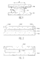
- the etching of the sacrificial layer is carried out chemically. After such etching, the delicate problem of drying the solvent used for rinsing the structure arises. In fact, during drying, the moving parts are subjected to attractive forces induced by the curvature of the liquid vapor solvent interface, as shown in FIG. 1. These capillary forces come from the surface tension of the rinsing liquid. in balance with its vapor on the solid.
- Figure 1 is a very schematic section of a micromechanical structure being dried after the chemical removal of a sacrificial layer. Between the parts 10 and 12 of this structure, initially connected by the sacrificial layer is a residue 14 of solvent.
- the angles of wetting at the liquid / solid / vapor triple points are designated by ⁇ 1 and ⁇ 2, by b the length of the liquid / solid interface and by d the distance between parts 10 and 12.
- q ⁇ . (cos ⁇ 1 + cos ⁇ 2 ).
- b d where ⁇ is the liquid / solid surface tension.
- the distance d decreases due to capillary forces acting on the parts 10 and 12. This has the effect of increasing these same forces, until the inevitable bonding of the moving parts 10 and 12
- the forces of attraction become of the Van Der Walls type, and the bonding becomes irreversible.
- Another possibility to avoid sticking between parts of a structure, separated by elimination of a sacrificial layer, consists in limiting the surfaces in contact with these parts during drying, and thus, making the drying reversible. For this it is sufficient that restoring forces acting on the part (s) (mobile) are greater than the attractive forces which are proportional to the surface of the parts in contact.
- Wiegand proposes an accelerometer with capacitive detection consisting of three substrates which are machined independently and then sealed.
- the central substrate constitutes a seismic mass, while the upper and lower substrates have stops which limit the contact surface with the seismic mass in the event of approach.
- Wilner proposes the same type of assembly but by placing the stops on the central substrate in which the seismic mass is machined.
- micromechanics are monocrystalline silicon.
- silicon on insulator type substrates are often used. These substrates consist of a silicon substrate covered with a thin layer of insulator, generally silica, which is itself covered with a thin layer of monocrystalline silicon.
- the insulating layer acts as a sacrificial layer, so that it is impossible to machine the surfaces liable to come into contact. Most of the techniques described above and making it possible to avoid sticking are therefore no longer applicable.
- An object of the present invention is precisely to propose a method for separating a useful layer of material initially connected to a substrate by a sacrificial layer, making it possible to avoid the problems of bonding mentioned above.
- Another object of the present invention is also to propose a method of manufacturing a structure comprising a useful layer kept at a distance from a substrate by stops, which is both compatible with the techniques of structures of the silicon on insulator type. , microelectronics techniques and with the requirements of manufacturing structures with very thin sacrificial layers.
- the useful layer constitutes for example the sensitive element of a sensor, such as a seismic mass of an accelerometer, or a membrane of a sensor of pressure. It can also be a mobile part such as the rotor of a micromotor for example.
- the first and second etchings can be carried out wet through at least one opening made in the useful layer.
- the distribution of the stops on at least one of the surfaces facing the useful layer and / or the substrate can be carried out by a given arrangement of the openings allowing access to the intermediate layer and therefore its etching.
- the number of stops formed is minimized and their distribution is adapted to give them maximum efficiency.
- the number and the distribution of the stops can advantageously be chosen so that the parts facing the useful layer and the substrate cannot have a deflection deflection greater than a predetermined final distance which must separate them.
- the first etching can be carried out from each opening, over a distance D substantially equal to, The 2 , where L is the maximum distance between neighboring openings and e is a characteristic dimension, for example the width of the stops.
- substrate is understood to mean either a thick layer serving as a support for the useful layer or a second useful layer which must be separated from the useful layer mentioned above.
- the initial structure can be of the silicon on insulator type.
- Such a structure has the advantage of being usual in microelectronic techniques and therefore perfectly compatible with the invention.
- the method can be applied to the manufacture of an accelerometer.
- the useful layer and the substrate are equipped with electrical means for measuring a relative displacement of this useful layer relative to the substrate under the effect of an acceleration.
- the useful layer forms the sensitive mobile mass of such an accelerometer.
- FIG. 2 shows a structure comprising a substrate 100, for example of silicon, a sacrificial layer 110 of silicon oxide collected in the substrate 100 and a so-called useful layer 120 of silicon, covering the sacrificial layer.
- An edge 130 of the substrate laterally surrounds the sacrificial layer.
- a first step consists in making openings 132, for example in the useful layer 120 in order to constitute access routes to the sacrificial layer 110.
- these openings are made in the useful layer 120 by taking advantage of an etching operation intended to shape the useful layer.
- the access routes are used for etching the layer 110.
- the etching can be carried out by attacking this layer 110 through the openings 132 with hydrofluoric acid .
- one or more blocks forming spacers remain between the substrate 100 and the useful layer 120.
- Such a block is represented in FIG. 3 with the reference 140.
- One or more blocks thus formed make it possible to maintain the substrate 100 and the useful layer 120 at a distance equal to the thickness of the initial sacrificial layer.
- a second selective etching for example with a potash solution, makes it possible to attack the substrate and the useful layer in the space which separates them. During this second etching which does not attack the blocks 140, these form masks and protect the regions of the substrate and of the useful layer on which they are supported.
- stops 150, 151 are formed respectively on the useful layer and on the on the substrate. These stops are shown in FIG. 4.
- the stops 150 and 151 face each other and are separated by the block 140.
- the substrate and the useful layer are made of different materials, of attack only one of these parts during the second engraving. It is thus also possible to selectively form stops either on the substrate or on the useful layer.
- a last step consists, as shown in FIG. 5, in eliminating during a third etching, the blocks 140 remaining between the stops 150 and 151.
- a spacing is maintained between the useful layer and the substrate by means of the stops 150 and 151.
- the width of this spacing depends on the height of the stops and therefore on the conditions (depth) of the second etching.
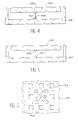
- FIG. 6 gives an example of an etching pattern for the openings 132 in the useful layer in order to produce central stops as shown in FIG. 5.
- Squares with the reference 133 correspond to the openings 132 made in the layer 120 to leave a central block 140 of dimension e.
- L On the checkerboard formed by the openings, L also designates the distance along a diagonal between the neighboring openings. As indicated above in the description, the first etching is carried out over a distance substantially equal to (L-e) / 2, measured parallel to the plane of the layer 120.
- the size of the stops and the blocks is not determined by photolithography, but by checking the kinetics of the engravings. This makes it possible to produce stops with dimensions of the order of a micrometer or less than a micrometer.
- the parameters which determine the dimensions and the height of the stops are therefore the same as those which govern any chemical etching kinetics, that is to say the concentration of reactive species, the temperature and the time.
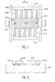
- a particular example of application of the above method is the production of a capacitive detection accelerometer with a sensitive axis parallel to the substrate.
- FIG. 7 is a top view of such an accelerometer. This comprises a mobile seismic mass 220, with fingers 222, 223 interdigitated with combs 201, 202 constituting fixed parts of the accelerometer.
- the seismic mass 220 moves in the direction of the acceleration ⁇ which is applied to it.
- this acceleration is represented by an arrow.
- the seismic mass is maintained by beams 226 having a stiffness k.
- the combs 201, 202 and the fingers 222, 223 of the seismic mass form the armatures of electrical capacitors.
- a displacement of the seismic mass corresponds for example to an increase in the capacity of the capacitor formed between the fingers 222 and the comb 201, denoted C 222-201 and a decrease in the capacity of the capacitor formed between the fingers 223 and the comb 202 denoted C 223-202 .
- the accelerometer of FIG. 7 is produced according to a planar manufacturing technique from a silicon-on-insulator type substrate.
- This type of substrate can be obtained either by implanting oxygen in an initial silicon substrate, or by sealing two substrates, one of which has been covered with a thin layer of silicon oxide. In both cases, the structure obtained consists of three layers: a very thick first layer of silicon, a second very thin sacrificial layer of silicon oxide and a third layer of silicon.
- the sacrificial layer of silicon oxide has a thickness of the order of 0.4 ⁇ m while the third layer, or upper layer has a thickness of 10 to 20 ⁇ m.
- the sensitive element of the accelerometer that is to say the mobile seismic mass 220 is delimited by photolithography in the third layer, and constitutes the useful layer within the meaning of the present invention.
- Openings 224 made in the useful layer in a pattern comparable to that of FIG. 6 constitute access routes to the sacrificial layer. These openings are made in the useful layer advantageously during the etching step of the third layer, defining the shape of the seismic mass.
- a first partial etching of the sacrificial layer is carried out with a hydrofluoric acid solution.
- Three blocks of the sacrificial layer designated with the reference 227 are preserved between the substrate and the useful layer, they have a section of the order of 1 ⁇ m.
- a selective etching of the silicon of the substrate and of the useful layer 220 is carried out with a potassium solution.
- the useful layer and the substrate are etched to a depth of the order of 0.1 ⁇ m on each of the facing faces. Stops are thus formed in the regions protected by the blocks 227.
- a final etching of the silicon oxide blocks is carried out with a hydrofluoric acid solution, taking care not to not alter the anchorages practiced on either side of the seismic mass too much.
- FIG. 8 After rinsing and drying, the structure of FIG. 8 is obtained.
- the substrate 200, the seismic mass 220, the beams 226 and the stops 228 produced in accordance with the method described above.
- the invention makes it possible, in very varied applications, to carry out a separation between parts of a micromechanical structure without risk of subsequent bonding of these parts. This is possible, thanks to the invention, without additional etching lithography step, and by involving only known chemical reactions and simple to carry out.
- the method of the invention can be implemented even in the case where the parts sensitive to sticking are not disposed on the surface of the structure.
Landscapes
- Engineering & Computer Science (AREA)
- Manufacturing & Machinery (AREA)
- Physics & Mathematics (AREA)
- General Physics & Mathematics (AREA)
- Microelectronics & Electronic Packaging (AREA)
- Pressure Sensors (AREA)
- Drying Of Semiconductors (AREA)
- Micromachines (AREA)
Applications Claiming Priority (2)
| Application Number | Priority Date | Filing Date | Title |
|---|---|---|---|
| FR9508882A FR2736934B1 (fr) | 1995-07-21 | 1995-07-21 | Procede de fabrication d'une structure avec une couche utile maintenue a distance d'un substrat par des butees, et de desolidarisation d'une telle couche |
| FR9508882 | 1995-07-21 |
Publications (2)
| Publication Number | Publication Date |
|---|---|
| EP0754953A1 true EP0754953A1 (de) | 1997-01-22 |
| EP0754953B1 EP0754953B1 (de) | 2001-06-20 |
Family
ID=9481249
Family Applications (1)
| Application Number | Title | Priority Date | Filing Date |
|---|---|---|---|
| EP96401625A Expired - Lifetime EP0754953B1 (de) | 1995-07-21 | 1996-07-19 | Verfahren zur Herstellung einer Struktur mit einer mittels Anschlägen auf Abstand von einem Substrat gehaltenen Nutzschicht, sowie Verfahren zur Loslösung einer solchen Schicht |
Country Status (5)
| Country | Link |
|---|---|
| US (1) | US5750420A (de) |
| EP (1) | EP0754953B1 (de) |
| JP (1) | JP3884795B2 (de) |
| DE (1) | DE69613437T2 (de) |
| FR (1) | FR2736934B1 (de) |
Cited By (4)
| Publication number | Priority date | Publication date | Assignee | Title |
|---|---|---|---|---|
| EP1857406A2 (de) * | 2006-05-16 | 2007-11-21 | Honeywell International Inc. | Herstellungsverfahren von Ausnehmungsstukturen zur Vermeidung der Haftreibung in einem MEMS-Bauteil. |
| EP2075224A2 (de) | 2007-12-27 | 2009-07-01 | Commissariat a L'Energie Atomique | Verfahren zur Herstellung eines mikomechanischen oder nanomechanischen Elements mit Anti-Haft-Anschlägen |
| EP2075223A2 (de) | 2007-12-27 | 2009-07-01 | Commissariat a L'Energie Atomique | Device with pre-released structure |
| CN101590995B (zh) * | 2008-05-27 | 2012-09-05 | 原相科技股份有限公司 | 同平面传感器 |
Families Citing this family (32)
| Publication number | Priority date | Publication date | Assignee | Title |
|---|---|---|---|---|
| DE4445177C5 (de) * | 1994-11-22 | 2015-09-17 | Fraunhofer-Gesellschaft zur Förderung der angewandten Forschung e.V. | Verfahren zur Herstellung mikromechanischer Bauelemente mit freistehenden Mikrostrukturen |
| WO1996023230A1 (de) * | 1995-01-24 | 1996-08-01 | Siemens Aktiengesellschaft | Mikromechanisches bauelement |
| US6035714A (en) * | 1997-09-08 | 2000-03-14 | The Regents Of The University Of Michigan | Microelectromechanical capacitive accelerometer and method of making same |
| FR2773261B1 (fr) | 1997-12-30 | 2000-01-28 | Commissariat Energie Atomique | Procede pour le transfert d'un film mince comportant une etape de creation d'inclusions |
| US6228275B1 (en) | 1998-12-10 | 2001-05-08 | Motorola, Inc. | Method of manufacturing a sensor |
| DE69916782D1 (de) * | 1999-02-26 | 2004-06-03 | St Microelectronics Srl | Verfahren zur Herstellung mechanischer, elektromechanischer und opto-elektromechanischer Mikrostrukturen mit aufgehängten Regionen welche während des Zusammenbaus mechanischen Spannungen ausgesetzt sind |
| US6316282B1 (en) | 1999-08-11 | 2001-11-13 | Adc Telecommunications, Inc. | Method of etching a wafer layer using multiple layers of the same photoresistant material |
| US6229640B1 (en) | 1999-08-11 | 2001-05-08 | Adc Telecommunications, Inc. | Microelectromechanical optical switch and method of manufacture thereof |
| US6242363B1 (en) * | 1999-08-11 | 2001-06-05 | Adc Telecommunications, Inc. | Method of etching a wafer layer using a sacrificial wall to form vertical sidewall |
| US6437965B1 (en) * | 2000-11-28 | 2002-08-20 | Harris Corporation | Electronic device including multiple capacitance value MEMS capacitor and associated methods |
| FR2823599B1 (fr) | 2001-04-13 | 2004-12-17 | Commissariat Energie Atomique | Substrat demomtable a tenue mecanique controlee et procede de realisation |
| US6801682B2 (en) | 2001-05-18 | 2004-10-05 | Adc Telecommunications, Inc. | Latching apparatus for a MEMS optical switch |
| WO2003055791A2 (en) * | 2001-10-17 | 2003-07-10 | Applied Materials, Inc. | Improved etch process for etching microstructures |
| AU2002258715A1 (en) * | 2002-04-04 | 2003-10-20 | Illusion Technologies, Llc | Miniature/micro scale power generation system |
| FR2848336B1 (fr) | 2002-12-09 | 2005-10-28 | Commissariat Energie Atomique | Procede de realisation d'une structure contrainte destinee a etre dissociee |
| US7122395B2 (en) * | 2002-12-23 | 2006-10-17 | Motorola, Inc. | Method of forming semiconductor devices through epitaxy |
| US6770506B2 (en) * | 2002-12-23 | 2004-08-03 | Motorola, Inc. | Release etch method for micromachined sensors |
| US6916728B2 (en) * | 2002-12-23 | 2005-07-12 | Freescale Semiconductor, Inc. | Method for forming a semiconductor structure through epitaxial growth |
| FR2856844B1 (fr) | 2003-06-24 | 2006-02-17 | Commissariat Energie Atomique | Circuit integre sur puce de hautes performances |
| FR2857002B1 (fr) * | 2003-07-04 | 2005-10-21 | Commissariat Energie Atomique | Procede de desolidarisation d'une couche utile et composant obtenu par ce procede |
| FR2857953B1 (fr) | 2003-07-21 | 2006-01-13 | Commissariat Energie Atomique | Structure empilee, et procede pour la fabriquer |
| US7087456B2 (en) * | 2003-10-07 | 2006-08-08 | Zyvex Corporation | Stiction resistant release process |
| FR2861497B1 (fr) | 2003-10-28 | 2006-02-10 | Soitec Silicon On Insulator | Procede de transfert catastrophique d'une couche fine apres co-implantation |
| JP4559273B2 (ja) * | 2005-03-30 | 2010-10-06 | シチズンファインテックミヨタ株式会社 | アクチュエータの製造方法 |
| FR2889887B1 (fr) | 2005-08-16 | 2007-11-09 | Commissariat Energie Atomique | Procede de report d'une couche mince sur un support |
| FR2891281B1 (fr) | 2005-09-28 | 2007-12-28 | Commissariat Energie Atomique | Procede de fabrication d'un element en couches minces. |
| US7939355B2 (en) * | 2005-10-13 | 2011-05-10 | The Regents Of The University Of California | Single-mask fabrication process for linear and angular piezoresistive accelerometers |
| US8084367B2 (en) * | 2006-05-24 | 2011-12-27 | Samsung Electronics Co., Ltd | Etching, cleaning and drying methods using supercritical fluid and chamber systems using these methods |
| FR2910179B1 (fr) | 2006-12-19 | 2009-03-13 | Commissariat Energie Atomique | PROCEDE DE FABRICATION DE COUCHES MINCES DE GaN PAR IMPLANTATION ET RECYCLAGE D'UN SUBSTRAT DE DEPART |
| FR2925221B1 (fr) | 2007-12-17 | 2010-02-19 | Commissariat Energie Atomique | Procede de transfert d'une couche mince |
| FR2947098A1 (fr) | 2009-06-18 | 2010-12-24 | Commissariat Energie Atomique | Procede de transfert d'une couche mince sur un substrat cible ayant un coefficient de dilatation thermique different de celui de la couche mince |
| FR2954505B1 (fr) | 2009-12-22 | 2012-08-03 | Commissariat Energie Atomique | Structure micromecanique comportant une partie mobile presentant des butees pour des deplacements hors plan de la structure et son procede de realisation |
Citations (5)
| Publication number | Priority date | Publication date | Assignee | Title |
|---|---|---|---|---|
| EP0386464A2 (de) | 1989-02-28 | 1990-09-12 | United Technologies | Kapazitiver Beschleunigungsmesser mit Kraftkompensation und vorgegebener Rückstellfederkraft |
| US4999735A (en) | 1990-03-08 | 1991-03-12 | Allied-Signal Inc. | Differential capacitive transducer and method of making |
| US5258097A (en) * | 1992-11-12 | 1993-11-02 | Ford Motor Company | Dry-release method for sacrificial layer microstructure fabrication |
| EP0605300A1 (de) * | 1992-12-28 | 1994-07-06 | Commissariat A L'energie Atomique | Verfahren zur Herstellung von Beschleunigungsmessern mittels der "Silizium auf Isolator"-Technologie sowie mittels diesem Verfahren erhaltener Beschleunigungsmesser |
| DE4317274A1 (de) * | 1993-05-25 | 1994-12-01 | Bosch Gmbh Robert | Verfahren zur Herstellung oberflächen-mikromechanischer Strukturen |
Family Cites Families (3)
| Publication number | Priority date | Publication date | Assignee | Title |
|---|---|---|---|---|
| US5203731A (en) * | 1990-07-18 | 1993-04-20 | International Business Machines Corporation | Process and structure of an integrated vacuum microelectronic device |
| US5397904A (en) * | 1992-07-02 | 1995-03-14 | Cornell Research Foundation, Inc. | Transistor microstructure |
| DE4315012B4 (de) * | 1993-05-06 | 2007-01-11 | Robert Bosch Gmbh | Verfahren zur Herstellung von Sensoren und Sensor |
-
1995
- 1995-07-21 FR FR9508882A patent/FR2736934B1/fr not_active Expired - Lifetime
-
1996
- 1996-07-10 US US08/676,629 patent/US5750420A/en not_active Expired - Lifetime
- 1996-07-19 JP JP19094096A patent/JP3884795B2/ja not_active Expired - Lifetime
- 1996-07-19 EP EP96401625A patent/EP0754953B1/de not_active Expired - Lifetime
- 1996-07-19 DE DE69613437T patent/DE69613437T2/de not_active Expired - Lifetime
Patent Citations (5)
| Publication number | Priority date | Publication date | Assignee | Title |
|---|---|---|---|---|
| EP0386464A2 (de) | 1989-02-28 | 1990-09-12 | United Technologies | Kapazitiver Beschleunigungsmesser mit Kraftkompensation und vorgegebener Rückstellfederkraft |
| US4999735A (en) | 1990-03-08 | 1991-03-12 | Allied-Signal Inc. | Differential capacitive transducer and method of making |
| US5258097A (en) * | 1992-11-12 | 1993-11-02 | Ford Motor Company | Dry-release method for sacrificial layer microstructure fabrication |
| EP0605300A1 (de) * | 1992-12-28 | 1994-07-06 | Commissariat A L'energie Atomique | Verfahren zur Herstellung von Beschleunigungsmessern mittels der "Silizium auf Isolator"-Technologie sowie mittels diesem Verfahren erhaltener Beschleunigungsmesser |
| DE4317274A1 (de) * | 1993-05-25 | 1994-12-01 | Bosch Gmbh Robert | Verfahren zur Herstellung oberflächen-mikromechanischer Strukturen |
Cited By (10)
| Publication number | Priority date | Publication date | Assignee | Title |
|---|---|---|---|---|
| EP1857406A2 (de) * | 2006-05-16 | 2007-11-21 | Honeywell International Inc. | Herstellungsverfahren von Ausnehmungsstukturen zur Vermeidung der Haftreibung in einem MEMS-Bauteil. |
| EP1857406A3 (de) * | 2006-05-16 | 2008-10-29 | Honeywell International Inc. | Herstellungsverfahren von Ausnehmungsstukturen zur Vermeidung der Haftreibung in einem MEMS-Bauteil. |
| EP2075224A2 (de) | 2007-12-27 | 2009-07-01 | Commissariat a L'Energie Atomique | Verfahren zur Herstellung eines mikomechanischen oder nanomechanischen Elements mit Anti-Haft-Anschlägen |
| EP2075223A2 (de) | 2007-12-27 | 2009-07-01 | Commissariat a L'Energie Atomique | Device with pre-released structure |
| FR2925889A1 (fr) * | 2007-12-27 | 2009-07-03 | Commissariat Energie Atomique | Procede de realisation d'un dispositif micromecanique et/ou nanomecanique a butees anti-collage |
| EP2075224A3 (de) * | 2007-12-27 | 2010-08-11 | Commissariat à l'Énergie Atomique et aux Énergies Alternatives | Verfahren zur Herstellung eines mikomechanischen oder nanomechanischen Elements mit Anti-Haft-Anschlägen |
| US8138556B2 (en) | 2007-12-27 | 2012-03-20 | Commissariat A L'energie Atomique | Pre-released structure device |
| EP2075223A3 (de) * | 2007-12-27 | 2012-06-27 | Commissariat à l'Énergie Atomique et aux Énergies Alternatives | Device with pre-released structure |
| US8557698B2 (en) | 2007-12-27 | 2013-10-15 | Commissariat A L'energie Atomique | Method for producing a micromechanical and/or nanomechanical device with anti-bonding stops |
| CN101590995B (zh) * | 2008-05-27 | 2012-09-05 | 原相科技股份有限公司 | 同平面传感器 |
Also Published As
| Publication number | Publication date |
|---|---|
| FR2736934B1 (fr) | 1997-08-22 |
| JP3884795B2 (ja) | 2007-02-21 |
| EP0754953B1 (de) | 2001-06-20 |
| JPH0936458A (ja) | 1997-02-07 |
| FR2736934A1 (fr) | 1997-01-24 |
| DE69613437T2 (de) | 2002-05-02 |
| DE69613437D1 (de) | 2001-07-26 |
| US5750420A (en) | 1998-05-12 |
Similar Documents
| Publication | Publication Date | Title |
|---|---|---|
| EP0754953B1 (de) | Verfahren zur Herstellung einer Struktur mit einer mittels Anschlägen auf Abstand von einem Substrat gehaltenen Nutzschicht, sowie Verfahren zur Loslösung einer solchen Schicht | |
| EP1835294B1 (de) | Dreiachsiger Beschleunigungsmesser mit Membran | |
| EP0605300B1 (de) | Verfahren zur Herstellung von Beschleunigungsmessern mittels der "Silizium auf Isolator"-Technologie | |
| EP1155442B1 (de) | Verfahren zur herstellung einer mehrschichtigen struktur mit kontrollierten eigenspannungen | |
| EP0605302B1 (de) | Herstellungsverfahren für Druckwandler mittels der Silicium auf Isolation Technologie sowie derart hergestellte Wandler | |
| EP2343556B1 (de) | Mikromechanische Struktur, die einen mobilen Teil mit Anschlägen für Bewegungen außerhalb der Planebene der Struktur umfasst, und ihr Herstellungsverfahren | |
| EP1677117B1 (de) | Mikromechanischer Beschleunigungsaufnehmer mit kapazitiven Kammstrukturen | |
| CN101152955B (zh) | 微结构器件的制造方法及其制造的微结构器件 | |
| EP2599746B1 (de) | Verfahren zur Herstellung einer Struktur mit mindestens einem aus mehreren Dicken bestehenden aktiven Teil | |
| EP1677118A1 (de) | Mikromechanischer Beschleunigungsaufnehmer mit kapazitiven Kammstukturen | |
| EP2808297B1 (de) | Verfahren zur Herstellung eines frei hängenden Teils einer mikro- und/oder nanoelektronischen Struktur in einem monolithischen Teil eines Substrats | |
| EP2546188B1 (de) | Verfahren zur Herstellung einer Struktur mit einer aufgehängten Membran und einer vergrabenen Elektrode | |
| EP2599745B1 (de) | Verfahren zum Herstellen eines MEMS Bauteil mit bewegliche Teile unterschiedlicher Dicke | |
| EP0983609B1 (de) | Verfahren zur herstellung eines mikrosensors mit mikrogefertigtem silizium | |
| FR3059312A1 (fr) | Procede de realisation d’un dispositif electromecanique | |
| FR2947096A1 (fr) | Procede de realisation d'une membrane plane | |
| EP2949621B1 (de) | Kapazitive mikro- und/ oder nanoelektronische Vorrichtung mit erhöhter Kompaktheit | |
| EP0950172B1 (de) | Verfahren zur herstellung eines aufgehängten elementes in einer mikromechanischen struktur | |
| EP2075223A2 (de) | Device with pre-released structure | |
| US20020073779A1 (en) | Semiconductor dynamic quantity detecting sensor and manufacturing method of the same | |
| FR3028257A1 (fr) | Procede de fabrication d'un dispositif electromecanique et dispositif correspondant | |
| FR2834282A1 (fr) | Procede de renforcement d'une microstructure mecanique | |
| EP3925930B1 (de) | Verfahren zur herstellung einer mikroelektronischen vorrichtung mit einer membran, die über einen hohlraum gespannt ist | |
| EP0611221A1 (de) | Kapazitiver Microsensor mit geringer Fremdkapazitanz und Herstellungsverfahren | |
| WO2002076881A1 (fr) | Procede de fabrication d'une structure a membrane micro-usinee |
Legal Events
| Date | Code | Title | Description |
|---|---|---|---|
| PUAI | Public reference made under article 153(3) epc to a published international application that has entered the european phase |
Free format text: ORIGINAL CODE: 0009012 |
|
| AK | Designated contracting states |
Kind code of ref document: A1 Designated state(s): DE GB IT |
|
| 17P | Request for examination filed |
Effective date: 19970626 |
|
| GRAG | Despatch of communication of intention to grant |
Free format text: ORIGINAL CODE: EPIDOS AGRA |
|
| 17Q | First examination report despatched |
Effective date: 20000204 |
|
| GRAG | Despatch of communication of intention to grant |
Free format text: ORIGINAL CODE: EPIDOS AGRA |
|
| GRAH | Despatch of communication of intention to grant a patent |
Free format text: ORIGINAL CODE: EPIDOS IGRA |
|
| GRAH | Despatch of communication of intention to grant a patent |
Free format text: ORIGINAL CODE: EPIDOS IGRA |
|
| GRAA | (expected) grant |
Free format text: ORIGINAL CODE: 0009210 |
|
| AK | Designated contracting states |
Kind code of ref document: B1 Designated state(s): DE GB IT |
|
| REF | Corresponds to: |
Ref document number: 69613437 Country of ref document: DE Date of ref document: 20010726 |
|
| ITF | It: translation for a ep patent filed |
Owner name: JACOBACCI & PERANI S.P.A. |
|
| GBT | Gb: translation of ep patent filed (gb section 77(6)(a)/1977) |
Effective date: 20010907 |
|
| REG | Reference to a national code |
Ref country code: GB Ref legal event code: IF02 |
|
| PLBE | No opposition filed within time limit |
Free format text: ORIGINAL CODE: 0009261 |
|
| STAA | Information on the status of an ep patent application or granted ep patent |
Free format text: STATUS: NO OPPOSITION FILED WITHIN TIME LIMIT |
|
| 26N | No opposition filed | ||
| PGFP | Annual fee paid to national office [announced via postgrant information from national office to epo] |
Ref country code: DE Payment date: 20150713 Year of fee payment: 20 Ref country code: GB Payment date: 20150717 Year of fee payment: 20 |
|
| PGFP | Annual fee paid to national office [announced via postgrant information from national office to epo] |
Ref country code: IT Payment date: 20150710 Year of fee payment: 20 |
|
| REG | Reference to a national code |
Ref country code: DE Ref legal event code: R071 Ref document number: 69613437 Country of ref document: DE |
|
| REG | Reference to a national code |
Ref country code: GB Ref legal event code: PE20 Expiry date: 20160718 |
|
| PG25 | Lapsed in a contracting state [announced via postgrant information from national office to epo] |
Ref country code: GB Free format text: LAPSE BECAUSE OF EXPIRATION OF PROTECTION Effective date: 20160718 |