EP0753842A2 - Thin film magnetic head including vias formed in alumina layer and process for making the same - Google Patents
Thin film magnetic head including vias formed in alumina layer and process for making the same Download PDFInfo
- Publication number
- EP0753842A2 EP0753842A2 EP96305196A EP96305196A EP0753842A2 EP 0753842 A2 EP0753842 A2 EP 0753842A2 EP 96305196 A EP96305196 A EP 96305196A EP 96305196 A EP96305196 A EP 96305196A EP 0753842 A2 EP0753842 A2 EP 0753842A2
- Authority
- EP
- European Patent Office
- Prior art keywords
- alumina
- layer
- etching
- metallic
- vias
- Prior art date
- Legal status (The legal status is an assumption and is not a legal conclusion. Google has not performed a legal analysis and makes no representation as to the accuracy of the status listed.)
- Withdrawn
Links
Images







Classifications
-
- C—CHEMISTRY; METALLURGY
- C04—CEMENTS; CONCRETE; ARTIFICIAL STONE; CERAMICS; REFRACTORIES
- C04B—LIME, MAGNESIA; SLAG; CEMENTS; COMPOSITIONS THEREOF, e.g. MORTARS, CONCRETE OR LIKE BUILDING MATERIALS; ARTIFICIAL STONE; CERAMICS; REFRACTORIES; TREATMENT OF NATURAL STONE
- C04B41/00—After-treatment of mortars, concrete, artificial stone or ceramics; Treatment of natural stone
- C04B41/009—After-treatment of mortars, concrete, artificial stone or ceramics; Treatment of natural stone characterised by the material treated
-
- C—CHEMISTRY; METALLURGY
- C04—CEMENTS; CONCRETE; ARTIFICIAL STONE; CERAMICS; REFRACTORIES
- C04B—LIME, MAGNESIA; SLAG; CEMENTS; COMPOSITIONS THEREOF, e.g. MORTARS, CONCRETE OR LIKE BUILDING MATERIALS; ARTIFICIAL STONE; CERAMICS; REFRACTORIES; TREATMENT OF NATURAL STONE
- C04B41/00—After-treatment of mortars, concrete, artificial stone or ceramics; Treatment of natural stone
- C04B41/53—After-treatment of mortars, concrete, artificial stone or ceramics; Treatment of natural stone involving the removal of at least part of the materials of the treated article, e.g. etching, drying of hardened concrete
- C04B41/5338—Etching
- C04B41/5353—Wet etching, e.g. with etchants dissolved in organic solvents
-
- C—CHEMISTRY; METALLURGY
- C04—CEMENTS; CONCRETE; ARTIFICIAL STONE; CERAMICS; REFRACTORIES
- C04B—LIME, MAGNESIA; SLAG; CEMENTS; COMPOSITIONS THEREOF, e.g. MORTARS, CONCRETE OR LIKE BUILDING MATERIALS; ARTIFICIAL STONE; CERAMICS; REFRACTORIES; TREATMENT OF NATURAL STONE
- C04B41/00—After-treatment of mortars, concrete, artificial stone or ceramics; Treatment of natural stone
- C04B41/80—After-treatment of mortars, concrete, artificial stone or ceramics; Treatment of natural stone of only ceramics
- C04B41/91—After-treatment of mortars, concrete, artificial stone or ceramics; Treatment of natural stone of only ceramics involving the removal of part of the materials of the treated articles, e.g. etching
-
- G—PHYSICS
- G11—INFORMATION STORAGE
- G11B—INFORMATION STORAGE BASED ON RELATIVE MOVEMENT BETWEEN RECORD CARRIER AND TRANSDUCER
- G11B5/00—Recording by magnetisation or demagnetisation of a record carrier; Reproducing by magnetic means; Record carriers therefor
- G11B5/127—Structure or manufacture of heads, e.g. inductive
- G11B5/31—Structure or manufacture of heads, e.g. inductive using thin films
- G11B5/3103—Structure or manufacture of integrated heads or heads mechanically assembled and electrically connected to a support or housing
-
- G—PHYSICS
- G11—INFORMATION STORAGE
- G11B—INFORMATION STORAGE BASED ON RELATIVE MOVEMENT BETWEEN RECORD CARRIER AND TRANSDUCER
- G11B5/00—Recording by magnetisation or demagnetisation of a record carrier; Reproducing by magnetic means; Record carriers therefor
- G11B5/127—Structure or manufacture of heads, e.g. inductive
- G11B5/31—Structure or manufacture of heads, e.g. inductive using thin films
- G11B5/3103—Structure or manufacture of integrated heads or heads mechanically assembled and electrically connected to a support or housing
- G11B5/3106—Structure or manufacture of integrated heads or heads mechanically assembled and electrically connected to a support or housing where the integrated or assembled structure comprises means for conditioning against physical detrimental influence, e.g. wear, contamination
-
- G—PHYSICS
- G11—INFORMATION STORAGE
- G11B—INFORMATION STORAGE BASED ON RELATIVE MOVEMENT BETWEEN RECORD CARRIER AND TRANSDUCER
- G11B5/00—Recording by magnetisation or demagnetisation of a record carrier; Reproducing by magnetic means; Record carriers therefor
- G11B5/127—Structure or manufacture of heads, e.g. inductive
- G11B5/31—Structure or manufacture of heads, e.g. inductive using thin films
- G11B5/3109—Details
- G11B5/313—Disposition of layers
-
- G—PHYSICS
- G11—INFORMATION STORAGE
- G11B—INFORMATION STORAGE BASED ON RELATIVE MOVEMENT BETWEEN RECORD CARRIER AND TRANSDUCER
- G11B5/00—Recording by magnetisation or demagnetisation of a record carrier; Reproducing by magnetic means; Record carriers therefor
- G11B5/127—Structure or manufacture of heads, e.g. inductive
- G11B5/31—Structure or manufacture of heads, e.g. inductive using thin films
- G11B5/3109—Details
- G11B5/313—Disposition of layers
- G11B5/3133—Disposition of layers including layers not usually being a part of the electromagnetic transducer structure and providing additional features, e.g. for improving heat radiation, reduction of power dissipation, adaptations for measurement or indication of gap depth or other properties of the structure
-
- G—PHYSICS
- G11—INFORMATION STORAGE
- G11B—INFORMATION STORAGE BASED ON RELATIVE MOVEMENT BETWEEN RECORD CARRIER AND TRANSDUCER
- G11B5/00—Recording by magnetisation or demagnetisation of a record carrier; Reproducing by magnetic means; Record carriers therefor
- G11B5/127—Structure or manufacture of heads, e.g. inductive
- G11B5/31—Structure or manufacture of heads, e.g. inductive using thin films
- G11B5/3163—Fabrication methods or processes specially adapted for a particular head structure, e.g. using base layers for electroplating, using functional layers for masking, using energy or particle beams for shaping the structure or modifying the properties of the basic layers
-
- G—PHYSICS
- G11—INFORMATION STORAGE
- G11B—INFORMATION STORAGE BASED ON RELATIVE MOVEMENT BETWEEN RECORD CARRIER AND TRANSDUCER
- G11B5/00—Recording by magnetisation or demagnetisation of a record carrier; Reproducing by magnetic means; Record carriers therefor
- G11B5/40—Protective measures on heads, e.g. against excessive temperature
-
- H—ELECTRICITY
- H10—SEMICONDUCTOR DEVICES; ELECTRIC SOLID-STATE DEVICES NOT OTHERWISE PROVIDED FOR
- H10P—GENERIC PROCESSES OR APPARATUS FOR THE MANUFACTURE OR TREATMENT OF DEVICES COVERED BY CLASS H10
- H10P95/00—Generic processes or apparatus for manufacture or treatments not covered by the other groups of this subclass
-
- C—CHEMISTRY; METALLURGY
- C04—CEMENTS; CONCRETE; ARTIFICIAL STONE; CERAMICS; REFRACTORIES
- C04B—LIME, MAGNESIA; SLAG; CEMENTS; COMPOSITIONS THEREOF, e.g. MORTARS, CONCRETE OR LIKE BUILDING MATERIALS; ARTIFICIAL STONE; CERAMICS; REFRACTORIES; TREATMENT OF NATURAL STONE
- C04B2111/00—Mortars, concrete or artificial stone or mixtures to prepare them, characterised by specific function, property or use
- C04B2111/00241—Physical properties of the materials not provided for elsewhere in C04B2111/00
- C04B2111/00422—Magnetic properties
-
- G—PHYSICS
- G11—INFORMATION STORAGE
- G11B—INFORMATION STORAGE BASED ON RELATIVE MOVEMENT BETWEEN RECORD CARRIER AND TRANSDUCER
- G11B19/00—Driving, starting, stopping record carriers not specifically of filamentary or web form, or of supports therefor; Control thereof; Control of operating function ; Driving both disc and head
- G11B19/02—Control of operating function, e.g. switching from recording to reproducing
- G11B19/04—Arrangements for preventing, inhibiting, or warning against double recording on the same blank or against other recording or reproducing malfunctions
-
- G—PHYSICS
- G11—INFORMATION STORAGE
- G11B—INFORMATION STORAGE BASED ON RELATIVE MOVEMENT BETWEEN RECORD CARRIER AND TRANSDUCER
- G11B5/00—Recording by magnetisation or demagnetisation of a record carrier; Reproducing by magnetic means; Record carriers therefor
- G11B5/127—Structure or manufacture of heads, e.g. inductive
- G11B5/31—Structure or manufacture of heads, e.g. inductive using thin films
- G11B5/3109—Details
- G11B5/313—Disposition of layers
- G11B5/3143—Disposition of layers including additional layers for improving the electromagnetic transducing properties of the basic structure, e.g. for flux coupling, guiding or shielding
-
- Y—GENERAL TAGGING OF NEW TECHNOLOGICAL DEVELOPMENTS; GENERAL TAGGING OF CROSS-SECTIONAL TECHNOLOGIES SPANNING OVER SEVERAL SECTIONS OF THE IPC; TECHNICAL SUBJECTS COVERED BY FORMER USPC CROSS-REFERENCE ART COLLECTIONS [XRACs] AND DIGESTS
- Y10—TECHNICAL SUBJECTS COVERED BY FORMER USPC
- Y10T—TECHNICAL SUBJECTS COVERED BY FORMER US CLASSIFICATION
- Y10T29/00—Metal working
- Y10T29/49—Method of mechanical manufacture
- Y10T29/49002—Electrical device making
- Y10T29/4902—Electromagnet, transformer or inductor
- Y10T29/49021—Magnetic recording reproducing transducer [e.g., tape head, core, etc.]
- Y10T29/49032—Fabricating head structure or component thereof
- Y10T29/49036—Fabricating head structure or component thereof including measuring or testing
- Y10T29/49043—Depositing magnetic layer or coating
- Y10T29/49046—Depositing magnetic layer or coating with etching or machining of magnetic material
Definitions
- This invention relates to magnetic thin film heads (TFH) for recording and reading magnetic transitions on a moving magnetic medium. It is applicable to either inductive or magnetoresistive (MR) elements.
- THF magnetic thin film heads
- MR magnetoresistive
- the invention relates to a method of etching deep vias through the thick alumina overcoat in order to expose underlying bonding pads, thereby completely eliminating fabrication of the studs (or bonding posts), a method of etching the undercoat to define scribe-line grooves of streets and alleys across the wafer for sawing (or dicing) and machining of the sliders, and a method of pattern-etching the alumina undercoat, prior to the wafer fabrication, to create precise craters for recessed structures or open vias to the substrate for lightning arresters.
- Magnetic TFH transducers are known in the prior art. See, e.g. U.S. Pat. Nos. 4,016,601; 4,190,872; 4,652,954; 4,791,719 for inductive devices and U.S. Pat. Nos. 4,190,871 and 4,315,291 for magnetoresistive (MR) devices.
- MR magnetoresistive
- a moving magnetic storage medium is placed near the exposed pole-tips of the TFH transducer.
- the changing magnetic flux of the moving storage medium induces a changing magnetic flux upon the pole-tips and the gap between them.
- the magnetic flux is carried through the pole-tips and yoke core around spiralling conductor coil winding turns located between the yoke arms.
- the changing magnetic flux induces an electrical voltage across the conductor coil.
- the electrical voltage is representative of the magnetic pattern stored on the moving magnetic storage medium.
- an electrical current is caused to flow through the conductor coil.
- the current in the coil induces a magnetic field across the gap between pole-tips.
- a fringe field extends into the nearby moving magnetic storage medium, inducing (or writing) a magnetic domain (in the medium) in the same direction. Impressing current pulses of alternating polarity across the coil causes the writing of magnetic domains of alternating polarity in the storage medium.
- Magnetoresistive (MR) TFH devices can only operate in the read mode.
- the electrical resistance of an MR element varies with its magnetization orientation. Magnetic flux from the moving magnetic storage medium induces changes in this orientation. As a result, the resistance of the MR element to a sensing electric current changes accordingly.
- the varying voltage signal is representative of the magnetic pattern stored on the magnetic medium.
- TFH transducers for magnetic recording
- a large number of devices are fabricated simultaneously in deposited and patterned layers on a ceramic wafer.
- the wafer is cut (or diced) and machined into individual slider transducers.
- the main elements of a TFH inductive transducer roughly in the order in which they are deposited, are the (alumina) undercoat, the bottom magnetic pole, the flux gap material to provide spacing between the bottom and top magnetic pole-tips, one or more levels of electrical conductive coil winding interposed within insulation layers, the top magnetic pole, elevated studs (or posts) for connecting the coil to bonding pads (above the overcoat), a thick (alumina) overcoat, and the bonding pads.
- the studs are made of about 25-50 ⁇ m thick copper, plated through a thick photoresist mask right after the completion of the top magnetic pole and prior to the deposition of thick alumina overcoat.
- the studs are designed to extend to a level about 10 ⁇ m above the highest spot of the TFH device (the back yoke of the top pole).
- the stud thickness must be increased by at least 6-9 ⁇ m.
- the alumina overcoat thickness must exceed the stud thickness by about 10 ⁇ m, requiring an overcoat about 35-60 ⁇ m thick.
- the studs are covered by the alumina overcoat. The wafer is then lapped (ground) down to expose the copper studs.
- (gold) bonding pads are fabricated over the alumina overcoat to contact the exposed studs.
- the pads are later used for bonding wires to external circuitry to the read/write channel.
- Fabrication of studs and bonding pads is described in U.S. Pat. No. 4,219,853, for example. It is similar in both inductive and MR devices. For TFH devices combining an inductive write element and an MR read element, one on top of the other, the stud and alumina overcoat operations have to be repeated. This may bring the total thickness of the studs to about 40-70 ⁇ m, and the total alumina overcoat thickness to about 50-80 ⁇ m.
- alumina deposition process is relatively slow, about 1-2 ⁇ m/hour, it can easily become the bottleneck (1-3 days) in the process flow. Furthermore, alumina sputtering equipment is very costly. As a result, the alumina overcoat deposition is by far the costliest and the slowest step in TFH wafer fabrication.
- the integrity and chipping resistance of the alumina overcoat are directly related to its thickness and stress.
- the alumina overcoat's stress also adversely affects the noise performance of the TFH device, since it is in direct contact with the top magnetic pole.
- tall features of the device, such as the studs impair the integrity of the deposited alumina in the local surrounding area. Sawing and machining operations subject the alumina overcoat to local stresses which often result in excessive chipping and rejects.
- stud plating dictates the use of a dry film photoresist which is difficult to strip and process.
- the usual fabrication of studs and bonding pads demands numerous steps of photomasking, deposition of seed-layers, plating, stripping, and etching.
- the elaborate structure of the studs and bonding pads, including coil leads, permalloy, and all the seed-layers, may involve some 10-15 individual metallic layers deposited in succession on top of each other. The probability of bonding failures due to inadequate adhesion between any two of these metallic layers is directly proportional to the number of these layers.
- the present invention provides an economical method for fast and precise patterning of thick sputter-deposited alumina layers by etching through appropriate metallic masks. It further provides improvements in product design and performance which avoid the above-described shortcomings of the prior art.
- the precise patterning of thick alumina layers by etching enables the fabrication of studless TFH devices, scribe-line grooves for dicing, recessed craters for TFH devices, and lightning arresters.
- Alumina chipping is usually a major contributor to yield loss. Etching scribe-line grooves facilitates significant reduction of alumina chipping during slider machining and later in tests and service. It thus significantly improves total device yields. Pattern-etching precise craters in the alumina undercoat facilitates the fabrication of TFH devices with recessed structures or features. These can improve device planarity and alleviate problems associated with tall features of multi-level coil designs.
- etching vias through the alumina undercoat layer enables the construction of lightning arresters by electrically connecting the magnetic core to the substrate, which will be grounded in the process of packaging the slider.
- the lightning arresters provide grounding to prevent arcing between the magnetic core and rotating disk.
- the patterning of thick sputter-deposited alumina layers is accomplished by, first, depositing compatible metallic layers on the alumina, coating the metallic layers with photoresist, patterning the photoresist by photolithography, etching the metallic layers (in sequence) through the photoresist mask, stripping the photoresist, wet chemical pattern-etching the thick alumina layer through the metallic mask, and removing (in sequence) the metallic masking layers.
- the etching can be conveniently performed by spray or immersion.
- a compatible metallic mask must be used with the dilute HF etchant since photoresist masks lift-off from the alumina surface after a very short time.
- a preferred metallic mask comprises a very thin (100-300 ⁇ ) Cr or Ti adhesion layer covered by a gold (Au) layer, about 0.3-0.5 ⁇ m thick. To avoid porosity in the gold layer and for economic reasons, at least one half of the gold thickness can be plated from an high purity (99.9%) "soft" gold bath.
- wet chemical etchants may also be used to pattern thick alumina layers. These may include hot phosphoric acid (H 3 PO 4 ) and hot strong bases such as KOH, NaOH, Ca(OH) 2 , and hot organic amines.
- a studless TFH device with gold coil and bonding pads, patterned and plated simultaneously is provided. Following the alumina overcoat deposition, vias are etched through it to expose the bonding pads. This eliminates copper altogether from the TFH device, resulting in less maintenance and significantly improved reliability, corrosion resistance, and consistency of the coil resistance. Similarly, the thick alumina is pattern-etched to form scribe-line grooves which minimize alumina chipping during sawing and machining. Other improvements in a TFH device resulting from deep alumina pattern-etching include the formation of recessed craters to improve planarity and pole-tips symmetry and the formation of vias to the substrate for lightning arresters connecting the magnetic core to the substrate.
- etching the alumina layer includes forming "plugs" over the bonding pads prior to the deposition of the alumina overcoat and then lapping the wafer to expose the plugs, which are then removed by selective etching (or stripping).
- Another alternative includes forming plugs with negative-slope walls prior to the deposition of the alumina layer, depositing the alumina layer, and dissolving the plugs with an appropriate selective etchant, thereby "lifting-off" the alumina overlying the plugs.
- vias etched in the alumina layer are partially or wholly filled with studs and bonding pads, or with bonding pads alone, thereby eliminating the need for the tip of the wire-bonding tool to fit entirely inside the vias when making the wire bonds.
- An object of this invention is to provide a method of pattern-etching through an alumina layer.
- Another object is to provide a studless TFH device.
- a further object of this invention is to provide a simple, fast, and low cost method to eliminate many processing steps and increase throughput in the process of fabricating a TFH device.
- An additional object is to significantly decrease alumina overcoat thickness to further reduce processing cost and improve reliability and throughput.
- Another object is to decrease alumina overcoat stress and related chipping and device noise.
- An additional object of this invention is to improve bonding strength and reliability by eliminating many metallic layers in the stud structure.
- An additional object is to eliminate dry photoresist processing.
- An additional object is to provide gold coil and bonding pads, fabricated simultaneously, to further delete some processing steps and to entirely eliminate copper material in the TFH device.
- Another object of the invention is to improve the corrosion resistance of a TFH device.
- a further object of the invention is to provide scribe-line grooves for dicing and slider machining to reduce alumina chipping and improve yields.
- Another object of the invention is to provide vias through the alumina undercoat to the substrate to enable the construction of lightning arresters.
- a still further object of this invention is to provide precise craters in the alumina undercoat to improve device planarity and pole-tips symmetry.
- a process for pattern-etching an alumina layer includes the steps of: depositing an alumina layer; depositing over the alumina layer an adhesion metallic layer; depositing over the adhesion metallic layer at least one additional metallic layer including a top metallic layer; forming a photoresist mask pattern over the top metallic layer; pattern-etching the top metallic layer through the photoresist mask; pattern-etching through the top metallic layer, in reverse order of deposition, the other metallic layer or layers; wet pattern-etching the alumina layer with a wet alumina etchant through the metallic layers; and removing the metallic layers.
- the process may also comprise a step of removing the photoresist mask following the step of pattern-etching the top metallic layer.
- the wet alumina etchant includes a chemical selected from the group consisting of HF, H 3 PO 4 , KOH, NaOH, Ca(OH) 2 , and strong organic amine bases.
- the wet alumina etchant may comprise a solution of HF in water.
- a process for forming a studless TFH device includes depositing and patterning bonding pads, depositing an alumina overcoat layer, and using the process of the first embodiment to etch vias in said alumina layer, said vias extending to the bonding pads.
- the step of depositing and patterning the bonding pads may comprise the step of simultaneously depositing and patterning both the coil and the bonding pads, the coil and the bonding pads comprising the same metal.
- the process may also comprise the step of depositing and patterning a coil, wherein the step of depositing and patterning the coil is separate from the step of depositing and patterning the bonding pads.
- the coil and the bonding pads may comprise metals, the metal comprised in the coil being different from the metal comprised in the bonding pads.
- the coil may comprise Al or Cu and the bonding pads comprise Au.
- the process may also comprise the steps of: depositing and patterning an intermediate metallic layer over the bonding pads following the step of depositing and patterning the bonding pads and prior to the step of depositing the alumina overcoat layer; and wherein the step of removing the metallic layers comprises the step of etching the intermediate metallic layer to expose the bonding pads.
- the step of depositing and patterning an intermediate metallic layer may comprise depositing a metal selected from the group consisting of Cr, Ti and Ni-Fe.
- a process for etching scribe-line grooves in a wafer containing a plurality of TFH devices includes using the process of the first embodiment to etch the scribe-line grooves through an alumina overcoat and an alumina undercoat, wherein a substrate serves as an etch-stopper.
- the step of etching the scribe-line grooves includes the step of etching vias through the alumina overcoat to the bonding pads.
- a process for etching a crater for a recessed structure in an alumina layer in a TFH device includes using the process of the first embodiment to etch the crater, wherein the depth of the crater is controlled by interrupting the etching action after a predetermined period of time.
- the crater depth may be controlled by placing an etch-stopper layer at a selected depth in the alumina layer.
- the etch-stopper layer may be selected from the group consisting of a metal, a cured photoresist, and a substrate.
- a process for constructing lightning arresters in a TFH device by etching vias through an alumina undercoat for connecting a magnetic core with a substrate includes using the process of the first embodiment to etch the vias, wherein the vias are etched through the alumina undercoat to expose the substrate, and including the further step of electrically connecting the magnetic core to the substrate through the vias.
- a process for constructing lightning arresters in a TFH device by etching vias through an alumina undercoat for connecting a magnetic core with a substrate includes using the process of the first embodiment to etch the vias, wherein a metallic layer is deposited over the substrate to serve as an etch-stopper, and including the further step of electrically connecting the magnetic core to the substrate through the vias and the metallic layer.
- a process for patterning an alumina layer includes the steps of: forming a pattern of plugs over a substrate, wherein said plugs comprise a material selected from the group consisting of photoresist and selectively etchable metals; depositing an alumina layer over said plugs; lapping-down said alumina layer to expose said plugs; and removing said plugs with a selective liquid etchant or stripper.
- a lift-off process for patterning an alumina layer includes the steps of: forming a pattern of plugs over a substrate, wherein said plugs comprise a material consisting of photoresist and selectively etchable metals, said plugs having negative-slope walls; depositing an alumina layer over said plugs, wherein the thickness of said alumina layer does not exceed the thickness of said plugs; selectively removing said plugs by applying a selective liquid etchant or stripper, thereby lifting-off a portion of the alumina layer overlying said plugs.
- the selectively etchable plugs may comprise a material selected from the group consisting of at least one photoresist layer and a selectively etchable metal.
- a process for forming a studless TFH device includes the step of depositing and patterning bonding pads, depositing an alumina overcoat layer, using the process of the eighth embodiment to form vias in the alumina layer, said vias extending to the bonding pads.
- a process for forming scribe-line grooves in a wafer comprising TFH devices includes using the process of the eighth embodiment to form the scribe-line grooves in an alumina layer, wherein said alumina layer comprises at least an alumina undercoat, and wherein said step of patterning the alumina layer comprises forming a scribe-line grooves pattern.
- a process for forming a crater for a recessed structure in an alumina layer in a TFH device includes using the process of the eighth embodiment to form the crater in an alumina layer, wherein said alumina layer is an alumina undercoat.
- a process for constructing lightning arresters in a TFH device by forming vias through an alumina undercoat so as to connect a magnetic core with a substrate includes using the process of the eighth embodiment to form vias in the alumina undercoat to expose the substrate, said process including the further step of electrically connecting the magnetic core to the substrate through the vias.
- a process for constructing lightning arresters in a TFH device by forming vias through an alumina undercoat so as to connect a magnetic core with a substrate includes depositing a metallic layer over the substrate and using the process of the eighth embodiment to form vias in the alumina undercoat to expose the metallic layer, said process including the further step of electrically connecting the magnetic core to the substrate through the vias and the metallic layer.
- a process for combining thick alumina vias and at least partial studs in a TFH device includes using the process of the first or eighth embodiment to form vias in an alumina overcoat layer, said process further including the step of depositing bonding pads inside said vias, said pads extending through at least a portion of the vias.
- a process for combining thick alumina vias and at least partial studs in a TFH device includes using the process of the first or eighth embodiment to form vias in an alumina overcoat layer, said process further including the steps of depositing studs inside said vias, said studs extending through at least a portion of said vias, and depositing bonding pads over said studs.
- a thin film head device may comprise a substrate, a coil lead, an overcoat layer disposed over said coil lead, a via opened in said overcoat layer and extending to said coil lead, a metallic stud in electrical contact with said coil lead and extending through said via part of the distance from said coil lead to a plane of a surface of said overcoat layer, a bonding pad formed over a surface of said metallic stud, and a wire bonded to said bonding pad.
- the thin film head device may comprise a substrate, a coil lead, an overcoat layer disposed over said coil lead, a via opened in said overcoat layer and extending to said coil lead, a metallic stud in electrical contact with said coil lead and extending through said via at least all the way from said coil lead to a plane of a surface of said overcoat layer, a bonding pad formed over a surface of said metallic stud, and a wire bonded to said bonding pad.
- Another thin film head device of the present invention comprises a substrate, a coil lead, an overcoat layer disposed over said coil lead, a via opened in said overcoat layer and extending to said coil lead, a bonding pad in electrical contact with said coil lead and extending through said via part of the distance from said coil lead to a plane of a surface of said overcoat layer, and a wire bonded to said bonding pad.
- the thin film head device may comprise a substrate, a coil lead, an overcoat layer disposed over said coil lead, a via opened in said overcoat layer and extending to said coil lead, a bonding pad in electrical contact with said coil lead and extending through said via at least all the way from said coil lead to a plane of a surface of said overcoat layer, and a wire bonded to said bonding pad.
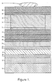
- Fig. 1 shows a cross-section of a typical prior-art stud and bonding pad structure.
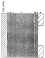
- Figs. 2(a) and 2(b) show cross-sections of alternative bonding pad structures embodying the present invention.
- Figs. 3(a) to 3(h) are cross-sectional views, at various stages, during the patterning of thick alumina, such as used for the studless pads of the present invention.
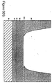
- Fig. 4 is a cross-sectional view of a scribe-line groove after pattern-etching.
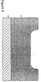
- Fig. 5 is a cross-sectional view of a recessed crater after pattern-etching.
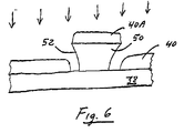
- Fig. 6 is a cross-sectional view showing the formation of a via in an alumina layer by lift-off process.
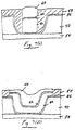
- Figs. 7(a) and 7(b) are cross-sectional views showing two ways in which a photoresist layer can be patterned to form a stud within a via.
- Fig. 8(a) is a cross-sectional view showing a stud and a bonding pad which extend partially through a via in an alumina layer.
- Fig. 8(b) is a cross-sectional view showing a stud and a bonding pad which extend all the way through a via in an alumina layer.
- Fig. 8(c) is a cross-sectional view showing a bonding pad which extends partially through a via in an alumina layer.
- Fig. 8(d) is a cross-sectional view showing a bonding pad which extends all the way through a via in an alumina layer.
- FIG. 1 A schematic (not to scale) cross-section of a typical prior-art stud and bonding pad structure is shown in Fig. 1.
- An alumina undercoat 12 is first deposited over a ceramic substrate 10. The wafer is then subjected to the deposition and patterning of many layers.
- a typical succession of the metallic layers in the stud area may include a Cr (or Ti) seed-layer 14, a Cu seed-layer 16, a first level plated Cu coil 18, a Cr (or Ti) seed-layer 20, a Cu seed-layer 22, a second level plated coil 24, a Ni-Fe seed-layer 26 for the top pole, a first plated Ni-Fe layer 28 of the top pole, a second plated Ni-Fe layer 30, a Cu seed-layer 32 for the stud, a plated Cu stud 34, alumina overcoat 35, a Ni-Fe seed-layer 36 for the bonding pad, and a gold bonding pad 38.
- a wire 39 is bonded to gold bonding pad 38, typically by thermocompression or ultrasonic compression techniques.
- the stud structure may include other layers, such as a Ni-Fe seed-layer and plated layers of the bottom pole (between layers 12 and 14), or a Cr (or Ti) seed-layer under Cu seed-layer 32 for the stud, or under Ni-Fe seed-layer 36 for the bonding pad, or under Ni-Fe seed-layer 26 for the pole plating. In other cases, several of these layers are omitted.
- the stud and bonding pad structure comprise about 10-15 individual metallic layers.
- the bonding pad structure is placed on the alumina overcoat in a partial overlapping and staggering position relative to the stud structure. Bonding is made to the off-set portion of the pad to ensure adequate bonding strength.
- Such elaborate structures of the studs and bonding pads are susceptible to bonding failure due to the large number of metallic layers in the structure. In addition, the poor integrity of the alumina overcoat in the region surrounding the tall stud further impairs reliability and bonding strength.
- the entire stud fabrication is eliminated, resulting in a simple bonding pad structure of only two metallic layers, shown in Fig. 2(a).
- a single seed-layer 36 such as Ni-Fe or W, is bonded to an alumina undercoat 12, which overlies a substrate 10.
- Seed layer 36 must be compatible for gold plating and must have good to moderate electrical conductivity and strong adhesion to alumina.
- Other metals and alloys suitable for this purpose include Mo, Ni-Co, Ni-Co-Fe, Cd, and In.
- the thickness of seed-layer 36 in Fig. 2(a) is in the range 600-2,000 ⁇ , and preferably in the range 1,000-1,500 ⁇ . This structure has only two metallic layers in the pad.
- An Au bonding pad 38 is preferably plated simultaneously with the coil turns and leads (not shown) through an appropriate photoresist mask. Both the coil and the bonding pads will then consist of the same (Au) metal. If the coil consists of more than a single level, different pads may be deposited and patterned simultaneously with different coil levels. Alternatively, one or more pads may be deposited and patterned repeatedly with more than one coil level. Such pads, however, will have more metallic layers in their structure. Following the coil/pad plating and stripping of the photoresist mask, seed-layer 36 must be removed from between the Au-plated areas. Using a different metal or alloy for seed-layer 36 from that used for pad 38 enables its removal by selective chemical etching, as described in U.S. Patent No. 5,059,278 to Cohen et al., incorporated herein by reference. Wire 39 is bonded to the (Au) bonding pad 38 through the etched vias in the alumina overcoat 40.
- the pad structure comprises a total of three or more metallic layers, as shown in Fig. 2(b).
- the structure combines at least two seed-layers.
- the first seed-layer comprises an adhesion layer 14 of Cr or Ti or another refractory metal such as W, Ta, Mo, Nb, V, Zr, and Hf, or an alloy comprising one or more of these metals.
- the function of this layer is to enhance adhesion between alumina and the following gold layer (gold alone has poor affinity to oxygen and, therefore, poor adhesion to alumina).
- the thickness of the adhesion seed-layer 14 can be in the range 50-500 ⁇ , and preferably in the range-100-300 ⁇ .
- the layer is usually deposited by a vacuum technique such as sputtering or evaporation.
- An Au seed-layer 37 is similarly deposited by sputtering or evaporation. It provides a low electrical resistance and compatible metallic surface for the plating of a gold pad 38.
- Other metals or alloys compatible with gold plating and having good electrical conductivity may also be used for the second metallic seed-layer 37. They include Ni-Fe, W, Mo, Cu, Ag, Pd, Pt, Rh, Ir, and alloys comprising one or more of these metals. In contrast, most refractory metals possess high electrical resistivity and are incompatible for gold plating.
- the thickness of the Au seed-layer 37 is in the range 500-3,000 ⁇ , and preferably in the range 700-1,000 ⁇ .
- Plated gold pad 38 has a thickness in the range 1.0-5.0 ⁇ m, and preferably in the range 2.0-4.0 ⁇ m.
- the coil turns and leads and bonding pads may be plated simultaneously through a suitable photoresist mask.
- the coil may comprise gold or another highly conductive metal which is deposited and patterned separately from the bonding pad 38.
- bonding pad 38 of Figs. 2(a) and 2(b) may comprise Au, Cu, Ag, Pd, Pt, Rh, Ir, and alloys comprising one or more elements thereof.
- the coil turns may comprise a different metal or alloy than the pad.
- the coil turns may comprise Cu, Ag, Pd, Pt, Rh, Ir, and alloys comprising one or more elements thereof, while the bonding pad may comprise gold.
- different metals or alloys in the coil and pads require further processing steps, which add to manufacturing complexity and cost.
- Al has both excellent conductivity and adhesion to alumina, it is incompatible for plating (of the coil). It is thus unsuitable as a seed-layer for any plating.
- Al as a single layer may be used simultaneously for both the coil and the bonding pad, if deposited by a vacuum technique (such as sputtering or evaporation) and patterned by etching.
- Appropriate etching techniques for Al patterning include ion milling and reactive ion etching (RIE). Wet etching of Al lacks the fine resolution required for the coil definition.
- the noble metals Au, Cu, Ag, Pd, Pt, Rh, Ir, and alloys comprising one or more metals thereof may also be deposited as a continuous layer by plating or by a vacuum technique, and then pattern-etched simultaneously for both the coil turns and pads by ion milling or by RIE.
- the dry etching technique requires an appropriate etch mask combining both the coil and the pads patterns. It is formed over the top continuous metal layer. The remains of the etch mask are removed following the dry etching.
- Top layer noble metals require an intermediate adhesion layer similar to seed layer 36 in Fig.
- the coil turns may comprise a different metal than the bonding pads and fabricated by different techniques.
- the coil turns may comprise sputter or evaporation deposited Al and may be patterned by ion milling or RIE, while the bonding pads may consist of plated gold.
- Patterning of thick alumina layers requires an etching mask which is substantially free of pores and not etched or adversely affected by the alumina etchant.
- etching masks based on photoresist alone are inadequate since they lift-off after only a short time in contact with the etchant.
- the dilute HF rapidly attacks the bond between the alumina and the photoresist.
- Metal masks must be used for the prolonged etching. The metal mask must have excellent adhesion to the alumina layer and it should be substantially free of pores. It must also be immune against attack by the etchant.
- FIG. 3(a) shows the structure after a photoresist layer 48 has been coated over the metallic mask layers and patterned by photolithography. Prior to coating the photoresist layer, successive seed-layers 42 of Cr or Ti and 44 of Au or Ni-Fe were deposited by a vacuum technique over a thick alumina layer 40. Seed-layer 42 must provide excellent adhesion to the alumina surface. It comprises a refractory metal from the group Cr, Ti, W, Ta, Mo, Nb, V, Zr, Hf, and alloys comprising one or more of these metals.
- the thickness of adhesion seed-layer 42 can be in the range 50-500 ⁇ , and preferably in the range 100-300 ⁇ . Since most refractory metals (such as Cr, Ti, Ta, Nb, V, Zr, and Hf) are incompatible for gold plating and have poor electrical conductivity, seed-layer 44, with good conductivity and compatibility for gold plating, is deposited over adhesion seed-layer 42. Gold is excellent for this purpose and is the preferred choice for seed-layer 44. However, it requires an expensive gold sputtering target.
- seed-layer 44 may comprise a metal from the group Ni-Fe, Ag, Pd, Pt, Rh, Ir, W, Mo, and alloys comprising one or more metals thereof.
- a single seed-layer 44 comprising Ni-Fe, W, Mo, or an alloy comprising one or more of these metals, possesses good adhesion and electrical conductivity and is compatible for gold plating. It can thus simplify the metallic mask by eliminating layer 42.
- the advantage of using Ni-Fe for seed-layer 44 is that it is already being utilized in the TFH fabrication process.
- the thickness of seed-layer 44 can be in the range 500-5,000 ⁇ , and preferably in the range 700-1,500 ⁇ .
- vacuum deposition produces layers 42 and 44 which are quite porous and permeable and, therefore, inadequate for use alone as the metallic mask for thick-alumina etching.
- the wafer After deposition of layers 42 and 44, the wafer is placed in a high purity (99.9%) "soft" gold plating bath, and a layer 46 of gold is plated over seed-layer 44.
- a layer 46 of gold is plated over seed-layer 44.
- its thickness should exceed about 0.1-0.2 ⁇ m.
- the thickness of layer 46 is in the range 0.1-1.0 ⁇ m, and preferably in the range 0.2-0.5 ⁇ m.
- sputter-deposited layers contain some pores even at thicknesses of more than 1.0 ⁇ m.
- thick ( ⁇ 2 ⁇ m) sputter-deposited Au layers significantly increase the manufacturing cost due to the very expensive gold targets.
- Photoresist mask layer 48 is coated over the metallic mask layers and patterned by a regular photolithography technique.
- Fig. 3(b) shows the structure after pattern-etching gold layers 46 and 44 through the photoresist mask.
- a convenient etchant for the gold layers is based on a dilute solution of KI and I 2 in water: Potassium Iodide KI 100 - 200 g/l Iodine I 2 25 - 50 g/l This etchant is compatible with the positive photoresist mask. It takes about 1-2 minutes to etch Au layers 46 and 44 using this etchant at room temperature. It can be applied by immersion with moderate agitation, or by spraying. Lower concentrations and temperature decrease the etch rate, while higher concentrations and temperature increase it.
- the pattern has to be further transferred by etching to the Cr or Ti adhesion layer 42.
- the photoresist layer 48 is removed using conventional stripping method, such as by dipping in or spraying with a commercial photoresist stripper, dilute KOH, or flood-light-exposure and developing.
- the wafer is placed in an appropriate selective etchant which only etches the Cr or Ti layer 42 but does not attack the Au mask.
- the photoresist is compatible with the etchant, it may be left in place during the etching of layer 42 and then removed.
- An appropriate etchant for Cr in layer 42 consists of a basic potassium ferricyanide: Potassium Hydroxide KOH 50 g/l Potassium Ferricyanide K 3 Fe (CN) 6 200 g/l
- This etchant is basic and, therefore, the (positive) photoresist mask is incompatible with it and must be removed prior to the etching. Using this etchant, it takes less than 1 minute to etch a Cr layer with thickness of 300 ⁇ at room temperature. This etchant may also be applied by immersion or by spraying. The wafer is now ready for the deep alumina etch.
- Fig. 3(c) shows the stage after etch-transfer through all the metallic layers and removal of the photoresist mask.
- Fig. 3(d) shows the structure after partial etching through the thick alumina layer.
- An excellent etchant for alumina layer 40 is based on dilute (1:2) HF in water: Hydrofluoric Acid (48%) HF 1 volume Water H 2 O 2 volumes This corresponds to an HF concentration by weight of 16%.
- the etchant is used by dipping with moderate agitation or by spraying. At room temperature the etch rate is about 1.0 ⁇ m/min. The etch rate is dependent on the quality, density, and integrity of the alumina layer. It is a function of sputter deposition parameters such as the substrate temperature, bias, gas pressure, power, and deposition rate. It is strongly affected by the local micro-topography and related alumina integrity.
- the etch rate of alumina of poor integrity in the vicinity of elevated features can be an order of magnitude faster than over a flat surface, far from the elevated features.
- dilute HF (1:2) etchant it was found that the etch rate across the wafer was highly uniform; ⁇ ⁇ 1%. This unusual etch uniformity is likely due to an interfacial kinetic control, as opposed to the more common mass transport control in most etching processes. The latter are sensitive to the degree of agitation, resulting in faster etching near edges and corners due to more vigorous agitation there.
- the interfacial reaction controlling the etching of alumina by dilute HF may involve the breaking of Al-O bonds in order to form soluble fluoride complex ions.
- the etch rate increases by raising the temperature or by using higher HF concentration. As the HF concentration decreases, the reaction kinetic becomes less interfacial controlled and more mass transport controlled.
- the operating temperature range can be 10-90°C, and preferably room temperature, for convenience.
- the etchant comprises HF and water in concentration range 10-100% v/v of concentrated (48%) HF, and preferably in the range 20-50% v/v of concentrated (48%) HF in water. The latter corresponds to a volume ratio range of 1:4 - 1:1 of (48%) HF and water and to a HF concentration in the range of 10% to 25% by weight.
- Other chemicals, such as alcohols or ethylene glycol, may also be added to or substituted for the water.
- etchants may also be used to pattern thick alumina layers. These may include hot phosphoric acid (H 3 PO 4 ) and hot strong bases such as KOH, NaOH, Ca(OH) 2 , and hot organic amines. In general, these etchants require relatively high concentrations and elevated temperatures to achieve reasonable etching rates, and they may lack the good uniformity of the HF-based etchant. Etch rates of the alternative etchants are sensitive to mass transport and therefore to agitation uniformity and to the aspect ratios of different features in the etch mask. Small features may etch slower than larger ones, leading to overetch of the latter. In general, the dry etching techniques, such as ion-milling or reactive ion etching (RIE), are too slow for etch-patterning thick alumina layers and are therefore impractical for this purpose.
- H 3 PO 4 hot phosphoric acid
- hot strong bases such as KOH, NaOH, Ca(OH) 2
- hot organic amines hot organic amines.
- Figs. 3(e) and 3(f) show the structure after completing the etching through the thick alumina layer 40 and after removal of the metallic mask layers, respectively.
- the Au bonding pad 38 serves as an etch stopper.
- the metallic mask layers are removed, in a reverse order of their deposition, by successive immersion or spraying first in a gold etchant (for layers 46 and 44) and then in a Cr (or Ti) etchant (for layer 42).
- the metallic mask layers can be removed by sputter-etching or ion-milling. These etching techniques will also etch a similar thickness of the Au pad 38. As Au pad 38 is much thicker than the mask layers, the slight decrease in its thickness is usually not significant.
- the initial thickness of pad 38 can be adjusted to compensate for this loss.
- a wet lift-off technique can be used, such as etching Cr layer 42 with an etchant based on acidic ceric ammonium sulfate (or nitrate) which rapidly attacks the bond between Cr layer 42 and alumina layer 40. This will cause the lift-off of the Au mask layers 44 and 46.
- An example of such an etchant is CR-14 manufactured by Cyantek Chemicals of Fremont, California.
- An alternative method to prevent etching of the Au pad 38 is to deposit and pattern an intermediate protective layer 38A of Cr (or Ti), as shown in Fig. 3(g), on top of the Au pad 38, prior to the deposition of alumina layer 40.
- the thickness of protective layer 38A is similar to that of layer 42 (about 100-300 ⁇ for Cr or Ti).
- the intermediate layer 38A protects Au pad 38 during the wet etching of Au layers 46 and 44.
- Protective layer 38A offers the additional benefit of improved adhesion to the thick alumina layer 40. It is then removed from the via area during the wet etching of Cr (or Ti) layer 42, exposing Au pad 38 for subsequent bonding, as shown in Fig. 3(h) .
- Protective layer 38A may also comprise a different metal or alloy than layer 42, such as plated or sputtered Ni-Fe. It can be etched by an appropriate selective etchant prior to or following the removal of layer 42.
- layer 38A may consist of a 500-2,000 ⁇ thick Ni-Fe layer plated immediately after the simultaneous plating of Au pad 38, using the same photoresist plating mask or another mask (exposing only the pad area).
- a selective etchant for this layer comprises nitric acid, phosphoric acid, and water in a volume ratio of 1:1:8, as described in U.S. Patent No. 5,059,278.
- a wire is bonded to Au bonding pad 38, typically by known thermocompression or ultrasonic compression techniques.
- a firm mechanical bond is then formed by surrounding the wire-pad bond with epoxy.
- the epoxy should preferably fill the via to the bonding pad so as to create an extremely strong mechanical bond between the wire and the TFH.
- Alumina integrity in the region around the bonding pad vias is not impaired by the etching action. It is similar to regions of the alumina layer removed from the vias, since it was not deposited over elevated features. Furthermore, due to the elimination of the studs the required alumina overcoat thickness is significantly reduced. It incorporates less (integrated) stress, resulting in less chipping during machining, testing, and service, and the noise level is lowered. Further benefits of the reduced alumina overcoat thickness include improved yields and reliability and significantly higher throughput and lower cost.
- Fig. 4 shows a scribe-line groove etched through the combined alumina layers of overcoat 40, gap 13, and undercoat 12 using similar methods of etching through thick alumina, as described above.
- the substrate 10 (usually comprising Al 2 O 3 -TiC) serves as the etch stopper. Removal of the sputter-deposited alumina in the wafer's streets and alleys grooves facilitates significant reduction of alumina chipping during the slider sawing and machining.
- the saw blade can be aligned precisely inside the grooves, without having to cut through the alumina layers, thereby maintaining alumina integrity and eliminating its chipping due to mechanical stress and damage.
- the etched scribe-line grooves also assist less wobble of the saw blade, preserving narrow cut lines and minimizing kerf.
- the scribe-line grooves can be etched during the same operation of etching the bonding pad vias, as described above.
- the combined groove and pad via mask pattern must be properly designed with smaller pad via openings to compensate for the lateral expansion during the extra etching time of the gap and undercoat layers.
- the combined etching of the bonding pad vias and scribe-lines has the further benefits of significantly reduced alumina overcoat layer thickness, shorter etch time, better resolution, improved alumina integrity (lower integrated stress and elimination of elevated features), improved yields and reliability, higher throughput, and lower cost.
- Fig. 5 shows a recessed crater formed in the alumina undercoat layer 12, using methods of etching through thick alumina similar to those described above.
- the crater depth can be controlled by removing the wafer from the etchant at any time before undercoat 12 has been etched through, or by placing an etch-stopper layer at the required depth.
- the etch-stopper may comprise a pore-free compatible metallic layer, cured photoresist layer, or the substrate itself. Due to the very uniform etch rate across the wafer, the craters are of very uniform depth. Alumina integrity in the vicinity and around the craters is not impaired by the etching action. It is similar to the bulk of the alumina layer far removed from the craters.
- Such craters can be used to fabricate in them at least a portion of the bottom magnetic pole, for example, in order to improve total device planarity and symmetry.
- Other device features or layers can also be fabricated inside such craters. These may include at least portions of the gap, one or more levels of insulation and/or coil layers or the metallic bonding pads.
- Lightning arresters can be constructed by etching vias through the alumina undercoat to expose the substrate and then electrically connecting the magnetic core to the substrate. Electrical connection between the magnetic core and the substrate is established by depositing and patterning a metallic layer through the vias following the alumina vias etching. Alternatively, a metallic layer may be deposited and patterned over the substrate prior to the deposition of the alumina undercoat. This metallic layer serves as the etch-stopper during the etching of the alumina vias. The metallic layer is connected through the vias to the magnetic core following the etching of the alumina vias, to insure good electrical contact between the magnetic core and the lightning arrester. Grounding the magnetic core electrically prevents arcing between the head and a rotating disk.
- the magnetic core is grounded by connecting it to the grounded substrate.
- the lightning arrester can be deposited and patterned either as part of the deposition of one of the magnetic poles, or it can be constructed as a separate layer preceding or following the deposition of either the bottom or the top magnetic pole.
- thick alumina layers can be patterned by non-etching techniques.
- One such alternative includes forming thick "plugs" over the bonding pads prior to the deposition of the alumina layer.
- the plugs may comprise photoresist or a selectively etchable metal. Following the deposition of the alumina layer, the wafer is lapped-down to expose the plugs, which are then removed by selective etching (or stripping).
- the technique requires the full thickness of the alumina overcoat, and it may produce inferior alumina integrity in the vicinity of the vias. Also, when using photoresist plugs, if the heat removal is inadequate during the alumina deposition, the photoresist may contaminate the sputtering system, or the plugs may bake beyond stripping.
- Other alternative non-etching methods to produce thick alumina layer patterning, or vias include various "lift-off" techniques. Such techniques require forming plugs with negative-slope walls prior to the deposition of the alumina layer.
- Fig. 6 shows a plug 50 having negative-slope walls 52 formed on a bonding pad 38. When alumina layer 40 is sputtered, a cap 40A is formed on top of plug 50.
- Lift-off methods may use, for example, (negative) photoresist plugs with negative-slope walls or selectively etchable metal plugs with negative-slope walls.
- the negative-slope walls of the plugs are required in order to provide accessibility of the liquid etchant (or stripper) to the plugs.
- the plugs must not be completely buried by the surrounding alumina layer. This implies that the plugs must be thicker than the deposited alumina layer.
- Photoresist plugs having the negative-slope walls can be produced by using a negative photoresist (or a positive photoresist with tone-reversal process). Alternatively, stacking two or more photoresist layers wherein the bottom photoresist layer is faster (more sensitive) and/or develops faster than the top photoresist layer, can produce negative-slope walls.
- Metal plugs with negative-slope walls can be produced by plating the metal through a positive photoresist mask and then stripping off the mask. The natural positive-slope wall profile of the positive photoresist mold mask produces a negative-slope wall profile of the plated metal plugs. Also, the metal plugs can be plated to a thickness well beyond the thickness of the photoresist mask, thereby causing the plugs to spread laterally (mushroom) over the photoresist mask.
- the lift-off methods generally require more processing steps than the etching methods and also may result in inferior alumina integrity in the vicinity of the vias.
- the lift-off methods offer the possibility of using a thinner alumina overcoat than is necessary for conventional studs.
- vias in the alumina overcoat are combined with studs which partially or completely fill the vias.
- the studs may be confined laterally to the central portion of the via, as shown in Fig. 7(a), or they may extend laterally to the sides of the via and beyond, as shown in Fig. 7(b).
- a seed or adhesion layer 56 is deposited on the exposed surfaces of the coil lead 54 and the alumina layer 40.
- a photoresist layer 58 is then deposited.
- photoresist layer 58 is photolithographically patterned such that it extends into the via, whereas in the embodiment of Fig.
- FIG. 7(b) it is patterned such that it is held back from the sides of the via.
- a metallic stud 60 is plated on the seed layer 56, and optionally a second seed layer 62 is deposited on the stud 60.
- a bonding pad 64 is then deposited on the seed layer 62. It will be evident that there are many possible embodiments between those shown in Figs. 7(a) and 7(b), with the stud having various widths. The embodiment of Fig. 7(a) is preferred, however, and will be used in the discussion which follows.
- FIGs. 8(a)-8(d) Various versions of the combination vias-studs technique are illustrated in Figs. 8(a)-8(d).
- a via is first formed in the alumina overcoat 40 to expose the coil lead 54
- a metallic stud 60 is plated inside the via
- a bonding pad 64 is formed over the stud 60.
- a wire 66 is bonded to the bonding pad 64.
- Seed layers 56 and 62 may be required between the coil lead 54 and metallic stud 60, and between the metallic stud 60 and bonding pad 64, respectively.
- Fig. 8(a)-8(d) Various versions of the combination vias-studs technique are illustrated in Figs. 8(a)-8(d).
- a via is first formed in the alumina overcoat 40 to expose the coil lead 54
- a metallic stud 60 is plated inside the via
- a bonding pad 64 is formed over the stud 60.
- a wire 66 is bonded to the bonding pad 64.
- the stud 60 extends part of the distance between the coil lead 54 and the plane of the surface of the alumina overcoat 40 (shown by the dashed line), whereas in Fig. 8(b) the stud extends all the way to the plane of the surface-of the alumina overcoat, and in other embodiments it could extend above the plane of the surface.
- the bonding pad 64 can be plated directly over the coil lead 54 (or over seed layer 56) at the bottom of the via to any required thickness without a separate stud plating, in which case the bonding pad serves in essence as both a bonding pad and as a partial- or full-height stud inside the via.
- the bonding pad 64 extends part of the distance between the coil lead 54 and the plane of the surface of the alumina overcoat 40, whereas in Fig. 8(c) the bonding pad 64 extends all the way to the plane of the surface of the alumina overcoat, and in other embodiments it could extend above the plane of the surface.
- the combination vias-studs scheme may alleviate problems arising from the dimensions of the wire bonding tool tip, since in the studless structure the bonding tool tip must readily fit inside the vias. This may be particularly important for very small form TFH devices, where the dimensions of the bonding pads and vias must be minimized.
- the combination method may utilize a relatively thin alumina overcoat and, provided that the alumina vias are formed by etching, the combination method can also provide good alumina integrity surrounding the vias. In general, however, methods which use a combination of vias and studs require significantly more processing and photomasking steps then the studless method.
- Bonding pad vias were etched through the alumina overcoat using a metallic etch mask similar to the one shown in Fig. 3(a).
- the Au pad 38 was 3.2 ⁇ m thick and the alumina overcoat 40 was about 35 ⁇ m thick.
- a 300 ⁇ thick Cr seed-layer 42 was sputter deposited over the alumina layer 40. This was immediately followed by sputtering a 1,000 ⁇ thick Au seed-layer 44.
- the wafer was then placed in a high purity "soft" gold plating bath (PAG 401, by Sel Rex) and was plated with a 5,000 ⁇ thick gold layer 46.
- a positive photoresist layer 48 was then coated, exposed and patterned with the pad areas opened, by a regular photolithographic process.
- the wafer was then placed in a gold etchant comprising KI (200 g/l), I 2 (50 g/l), and pure water. Etching was done at room temperature by immersion with moderate agitation. Inspection after 60 seconds etching revealed that the gold was cleared in the via areas, as shown in Fig. 3(b). An extra etching time of 30 seconds was used to ensure complete Au etching everywhere. Photoresist mask 48 was then removed using successive immersions in hot and cold acetone with moderate agitation. The thickness of the Au layer across the wafer was measured with a Dektak surface profilometer. Next, the Cr seed-layer 42 was pattern-etched using the gold layers 44 and 46 as etch mask.
- the etchant comprised KOH (50 g/l), K 3 Fe(CN) 6 (200 g/l), and pure water. Etching was carried out by immersion with moderate agitation at room temperature. Inspection after 35 seconds of etching revealed that the Cr was cleared in the via areas, as shown in Fig. 3(c). An extra etching time of 90 seconds was used to ensure complete etching. This completed the pattern transfer to the metal mask. The wafer was then immersed with moderate agitation in dilute HF (1:2) in water at room temperature to etch the alumina layer 40. Etching was interrupted after a partial etching of 30 minutes, as shown in Fig. 3(d).
- Example 2 The configuration and etching procedures were used as in Example 1, except that the plated Au layer 46 was only about 0.2 ⁇ m thick. Also, a single sputter-etching step was used to remove all the metallic mask layers after completion of the alumina etching. Again, even with the thinner Au mask layer, no pin-holes or other defects were observed in the protected areas and line definition was excellent.
- the wafers of Examples 1 and 2 were tested for bonding strength.
- Gold plated Cu wires were bonded through the alumina vias to the gold pads. Bonding tool alignment (to the pads) and whipping were greatly eased by the vias.
- the bonding strength of these studless devices was compared by a pull-test against regularly fabricated devices with thick copper studs. The studless devices exhibited excellent bonding strength, over 65 grams force in the pull-test. In all tests of the studless devices the applied force was either the maximum deliverable by the tester, or failures were attributable to wire breaking. For comparison, the regular devices with studs exhibited failures at about 28-35 grams force, with failures often due to bond breaking.
- Scribe-line grooves were etched through the alumina overcoat, gap, and undercoat layers using a metallic etch mask similar to that used in Examples 1 and 2, but with a sputtered 1,000 ⁇ thick Ni-Fe seed-layer (44 in Fig. 3(a)) instead of an Au seed-layer.
- the substrate 10 itself served as the alumina etch stopper, see Fig. 4.
- the thickness of the combined alumina layers was about 55 ⁇ m, and the plated Au layer 46 was about 5,000 ⁇ thick.
- the Ni-Fe seed-layer was pattern-etched by an etchant comprising 1 volume of (concentrated) nitric acid, 1 volume of (concentrated) phosphoric acid, and 8 volumes of pure water, as described in U.S. Patent No. 5,059,278. Etching was done by immersion with moderate agitation and at room temperature. Etching duration was 4.0 minutes to ensure complete clearing of the Ni-Fe in the groove areas.
- the photoresist mask 48 was then removed by dipping in a 5% (w/o) KOH solution in water, at room temperature and with moderate agitation.
- the Cr seed-layer 42 was pattern-etched as in Examples 1 and 2.
- the thickness of the combined metallic mask layers was then measured across the wafer by a Dektak profilometer.
- the combined alumina layers were then etched in the dilute HF (1:2) etchant, similar to Examples 1 and 2.
- Alumina etching was interrupted after 50 minutes, and the step height was measured by a Dektak profilometer across the wafer (in exactly the same spots as after the etching of the Cr mask layer).
- the wafer was then replaced in the alumina etchant for 5 more minutes and the step height measured again in the same locations.
- the wafer with the etched streets and alleys scribe-line grooves was sawed and machined into regular rows and sliders using the grooves as guides for the saw blade.
- Alumina chipping was compared against regular wafers without the scribe-line grooves. The latter showed significantly more alumina chipping than the first.
- the wafer with the etched alumina grooves displayed clean cuts with no detectable alumina chipping.
Landscapes
- Engineering & Computer Science (AREA)
- Chemical & Material Sciences (AREA)
- Ceramic Engineering (AREA)
- Manufacturing & Machinery (AREA)
- Materials Engineering (AREA)
- Organic Chemistry (AREA)
- Structural Engineering (AREA)
- Physics & Mathematics (AREA)
- Electromagnetism (AREA)
- Magnetic Heads (AREA)
- Manufacturing Of Printed Circuit Boards (AREA)
- Internal Circuitry In Semiconductor Integrated Circuit Devices (AREA)
- Weting (AREA)
- Hall/Mr Elements (AREA)
Abstract
Description
- This application is a continuation-in-part of Application No. 08/135,033, filed October 12, 1993, which is a divisional of Application No. 07/918,725, filed July 21, 1992, now U.S. Patent No. 5,326,429.
- This invention relates to magnetic thin film heads (TFH) for recording and reading magnetic transitions on a moving magnetic medium. It is applicable to either inductive or magnetoresistive (MR) elements.
- In particular, the invention relates to a method of etching deep vias through the thick alumina overcoat in order to expose underlying bonding pads, thereby completely eliminating fabrication of the studs (or bonding posts), a method of etching the undercoat to define scribe-line grooves of streets and alleys across the wafer for sawing (or dicing) and machining of the sliders, and a method of pattern-etching the alumina undercoat, prior to the wafer fabrication, to create precise craters for recessed structures or open vias to the substrate for lightning arresters.
- Magnetic TFH transducers are known in the prior art. See, e.g. U.S. Pat. Nos. 4,016,601; 4,190,872; 4,652,954; 4,791,719 for inductive devices and U.S. Pat. Nos. 4,190,871 and 4,315,291 for magnetoresistive (MR) devices.
- In the operation of a typical inductive TFH device a moving magnetic storage medium is placed near the exposed pole-tips of the TFH transducer. During the read operation, the changing magnetic flux of the moving storage medium induces a changing magnetic flux upon the pole-tips and the gap between them. The magnetic flux is carried through the pole-tips and yoke core around spiralling conductor coil winding turns located between the yoke arms. The changing magnetic flux induces an electrical voltage across the conductor coil. The electrical voltage is representative of the magnetic pattern stored on the moving magnetic storage medium. During the write operation, an electrical current is caused to flow through the conductor coil. The current in the coil induces a magnetic field across the gap between pole-tips. A fringe field extends into the nearby moving magnetic storage medium, inducing (or writing) a magnetic domain (in the medium) in the same direction. Impressing current pulses of alternating polarity across the coil causes the writing of magnetic domains of alternating polarity in the storage medium.
- Magnetoresistive (MR) TFH devices can only operate in the read mode. The electrical resistance of an MR element varies with its magnetization orientation. Magnetic flux from the moving magnetic storage medium induces changes in this orientation. As a result, the resistance of the MR element to a sensing electric current changes accordingly. The varying voltage signal is representative of the magnetic pattern stored on the magnetic medium.
- In the manufacturing of TFH transducers for magnetic recording, a large number of devices are fabricated simultaneously in deposited and patterned layers on a ceramic wafer. When completed, the wafer is cut (or diced) and machined into individual slider transducers. The main elements of a TFH inductive transducer, roughly in the order in which they are deposited, are the (alumina) undercoat, the bottom magnetic pole, the flux gap material to provide spacing between the bottom and top magnetic pole-tips, one or more levels of electrical conductive coil winding interposed within insulation layers, the top magnetic pole, elevated studs (or posts) for connecting the coil to bonding pads (above the overcoat), a thick (alumina) overcoat, and the bonding pads.
- Usually the studs are made of about 25-50µm thick copper, plated through a thick photoresist mask right after the completion of the top magnetic pole and prior to the deposition of thick alumina overcoat. For reasons of uniformity and reproducibility, the studs are designed to extend to a level about 10µm above the highest spot of the TFH device (the back yoke of the top pole). For each coil level the stud thickness must be increased by at least 6-9µm. For similar reasons, the alumina overcoat thickness must exceed the stud thickness by about 10µm, requiring an overcoat about 35-60µm thick. Following the overcoat deposition, the studs are covered by the alumina overcoat. The wafer is then lapped (ground) down to expose the copper studs. Next, (gold) bonding pads are fabricated over the alumina overcoat to contact the exposed studs. The pads are later used for bonding wires to external circuitry to the read/write channel. Fabrication of studs and bonding pads is described in U.S. Pat. No. 4,219,853, for example. It is similar in both inductive and MR devices. For TFH devices combining an inductive write element and an MR read element, one on top of the other, the stud and alumina overcoat operations have to be repeated. This may bring the total thickness of the studs to about 40-70µm, and the total alumina overcoat thickness to about 50-80µm. As the alumina deposition process is relatively slow, about 1-2µm/hour, it can easily become the bottleneck (1-3 days) in the process flow. Furthermore, alumina sputtering equipment is very costly. As a result, the alumina overcoat deposition is by far the costliest and the slowest step in TFH wafer fabrication.
- The integrity and chipping resistance of the alumina overcoat are directly related to its thickness and stress. The thicker the alumina layer, the more stress it incorporates. The alumina overcoat's stress also adversely affects the noise performance of the TFH device, since it is in direct contact with the top magnetic pole. Moreover, tall features of the device, such as the studs, impair the integrity of the deposited alumina in the local surrounding area. Sawing and machining operations subject the alumina overcoat to local stresses which often result in excessive chipping and rejects.
- Very thick studs require a relatively long plating time and the thickness uniformity is quite difficult to control. To achieve the required thickness, stud plating dictates the use of a dry film photoresist which is difficult to strip and process. The usual fabrication of studs and bonding pads demands numerous steps of photomasking, deposition of seed-layers, plating, stripping, and etching. The elaborate structure of the studs and bonding pads, including coil leads, permalloy, and all the seed-layers, may involve some 10-15 individual metallic layers deposited in succession on top of each other. The probability of bonding failures due to inadequate adhesion between any two of these metallic layers is directly proportional to the number of these layers. Thus reliability of the bond strength is adversely affected by the large number of the metallic layers in the structure. The poor integrity of the alumina overcoat in the locales surrounding the studs further degrades the bond strength and often impairs the fabrication of bonding pads due to "loops" of collapsed alumina around the studs. The latter appear following the lapping of the alumina overcoat to expose the studs, and are due to the poor integrity of the alumina surrounding the studs.
- Copper residues and contamination, originating from copper seed-layers used for the coil and stud platings, may cause shorts and impair the corrosion resistance of the TFH device. Copper coil seed-layer residues are often found to be responsible for intensified corrosion susceptibility of exposed pole-tips in the air bearing surface (ABS). This poor corrosion resistance is due to galvanic action between the two dissimilar metals (Cu and Ni-Fe) contacting at the corners (or wings) of the pole-tips. Similarly, the copper seed-layer of the studs is often found to degrade coil-to-core resistance due to full or partial shorts. The copper coil itself is sometimes subject to capricious variations of its electrical resistance due to corrosion and oxidation of the copper turns during elevated temperature curing cycles of the photoresist insulation layers.
- The present invention provides an economical method for fast and precise patterning of thick sputter-deposited alumina layers by etching through appropriate metallic masks. It further provides improvements in product design and performance which avoid the above-described shortcomings of the prior art. In particular, the precise patterning of thick alumina layers by etching enables the fabrication of studless TFH devices, scribe-line grooves for dicing, recessed craters for TFH devices, and lightning arresters.
- Elimination of the studs simplifies the wafer fabrication in a very substantial way. It curtails about 20-30% of the total wafer processing steps and reduces the alumina overcoat thickness by about 30-50%. It thus produces the substantial benefits of reducing processing costs, decreasing device noise, and improving throughput, consistency, bonding strength, and corrosion resistance. Alumina chipping is usually a major contributor to yield loss. Etching scribe-line grooves facilitates significant reduction of alumina chipping during slider machining and later in tests and service. It thus significantly improves total device yields. Pattern-etching precise craters in the alumina undercoat facilitates the fabrication of TFH devices with recessed structures or features. These can improve device planarity and alleviate problems associated with tall features of multi-level coil designs. They can also improve the symmetry of pole-tips configuration. Similarly, etching vias through the alumina undercoat layer enables the construction of lightning arresters by electrically connecting the magnetic core to the substrate, which will be grounded in the process of packaging the slider. The lightning arresters provide grounding to prevent arcing between the magnetic core and rotating disk.
- In accordance with this invention, the patterning of thick sputter-deposited alumina layers is accomplished by, first, depositing compatible metallic layers on the alumina, coating the metallic layers with photoresist, patterning the photoresist by photolithography, etching the metallic layers (in sequence) through the photoresist mask, stripping the photoresist, wet chemical pattern-etching the thick alumina layer through the metallic mask, and removing (in sequence) the metallic masking layers. A preferred etchant comprising dilute HF in water (1:2 by volume ratio) has been found to provide fast (about 1µm/min), extraordinarily uniform (better than σ = 1% across a wafer), and accurate etching of thick alumina layers. The etching can be conveniently performed by spray or immersion. A compatible metallic mask must be used with the dilute HF etchant since photoresist masks lift-off from the alumina surface after a very short time. A preferred metallic mask comprises a very thin (100-300Å) Cr or Ti adhesion layer covered by a gold (Au) layer, about 0.3-0.5µm thick. To avoid porosity in the gold layer and for economic reasons, at least one half of the gold thickness can be plated from an high purity (99.9%) "soft" gold bath.
- Other wet chemical etchants may also be used to pattern thick alumina layers. These may include hot phosphoric acid (H3PO4) and hot strong bases such as KOH, NaOH, Ca(OH)2, and hot organic amines.
- In accordance with the invention a studless TFH device with gold coil and bonding pads, patterned and plated simultaneously, is provided. Following the alumina overcoat deposition, vias are etched through it to expose the bonding pads. This eliminates copper altogether from the TFH device, resulting in less maintenance and significantly improved reliability, corrosion resistance, and consistency of the coil resistance. Similarly, the thick alumina is pattern-etched to form scribe-line grooves which minimize alumina chipping during sawing and machining. Other improvements in a TFH device resulting from deep alumina pattern-etching include the formation of recessed craters to improve planarity and pole-tips symmetry and the formation of vias to the substrate for lightning arresters connecting the magnetic core to the substrate.
- Several alternative embodiments which do not require etching the alumina layer are also disclosed. One such alternative includes forming "plugs" over the bonding pads prior to the deposition of the alumina overcoat and then lapping the wafer to expose the plugs, which are then removed by selective etching (or stripping). Another alternative includes forming plugs with negative-slope walls prior to the deposition of the alumina layer, depositing the alumina layer, and dissolving the plugs with an appropriate selective etchant, thereby "lifting-off" the alumina overlying the plugs.
- In an alternative embodiment, vias etched in the alumina layer are partially or wholly filled with studs and bonding pads, or with bonding pads alone, thereby eliminating the need for the tip of the wire-bonding tool to fit entirely inside the vias when making the wire bonds.
- An object of this invention is to provide a method of pattern-etching through an alumina layer.
- Another object is to provide a studless TFH device.
- A further object of this invention is to provide a simple, fast, and low cost method to eliminate many processing steps and increase throughput in the process of fabricating a TFH device.
- An additional object is to significantly decrease alumina overcoat thickness to further reduce processing cost and improve reliability and throughput.
- Another object is to decrease alumina overcoat stress and related chipping and device noise.
- An additional object of this invention is to improve bonding strength and reliability by eliminating many metallic layers in the stud structure.
- An additional object is to eliminate dry photoresist processing.
- An additional object is to provide gold coil and bonding pads, fabricated simultaneously, to further delete some processing steps and to entirely eliminate copper material in the TFH device.
- Another object of the invention is to improve the corrosion resistance of a TFH device.
- A further object of the invention is to provide scribe-line grooves for dicing and slider machining to reduce alumina chipping and improve yields.
- Another object of the invention is to provide vias through the alumina undercoat to the substrate to enable the construction of lightning arresters.
- A still further object of this invention is to provide precise craters in the alumina undercoat to improve device planarity and pole-tips symmetry.
- In one embodiment of the present invention, a process for pattern-etching an alumina layer, includes the steps of: depositing an alumina layer; depositing over the alumina layer an adhesion metallic layer; depositing over the adhesion metallic layer at least one additional metallic layer including a top metallic layer; forming a photoresist mask pattern over the top metallic layer; pattern-etching the top metallic layer through the photoresist mask; pattern-etching through the top metallic layer, in reverse order of deposition, the other metallic layer or layers; wet pattern-etching the alumina layer with a wet alumina etchant through the metallic layers; and removing the metallic layers. The process may also comprise a step of removing the photoresist mask following the step of pattern-etching the top metallic layer.
- Preferably, the wet alumina etchant includes a chemical selected from the group consisting of HF, H3PO4, KOH, NaOH, Ca(OH)2, and strong organic amine bases. For example, the wet alumina etchant may comprise a solution of HF in water.
- In a second embodiment of the present invention, a process for forming a studless TFH device includes depositing and patterning bonding pads, depositing an alumina overcoat layer, and using the process of the first embodiment to etch vias in said alumina layer, said vias extending to the bonding pads.
- The step of depositing and patterning the bonding pads may comprise the step of simultaneously depositing and patterning both the coil and the bonding pads, the coil and the bonding pads comprising the same metal. The process may also comprise the step of depositing and patterning a coil, wherein the step of depositing and patterning the coil is separate from the step of depositing and patterning the bonding pads. The coil and the bonding pads may comprise metals, the metal comprised in the coil being different from the metal comprised in the bonding pads. In particular, the coil may comprise Al or Cu and the bonding pads comprise Au. Further, the process may also comprise the steps of: depositing and patterning an intermediate metallic layer over the bonding pads following the step of depositing and patterning the bonding pads and prior to the step of depositing the alumina overcoat layer; and wherein the step of removing the metallic layers comprises the step of etching the intermediate metallic layer to expose the bonding pads. In this case, the step of depositing and patterning an intermediate metallic layer may comprise depositing a metal selected from the group consisting of Cr, Ti and Ni-Fe.
- In a third embodiment of the present invention, a process for etching scribe-line grooves in a wafer containing a plurality of TFH devices includes using the process of the first embodiment to etch the scribe-line grooves through an alumina overcoat and an alumina undercoat, wherein a substrate serves as an etch-stopper.
- Optionally, the step of etching the scribe-line grooves includes the step of etching vias through the alumina overcoat to the bonding pads.
- In a fourth embodiment of the present invention, a process for etching a crater for a recessed structure in an alumina layer in a TFH device includes using the process of the first embodiment to etch the crater, wherein the depth of the crater is controlled by interrupting the etching action after a predetermined period of time. The crater depth may be controlled by placing an etch-stopper layer at a selected depth in the alumina layer. Also, the etch-stopper layer may be selected from the group consisting of a metal, a cured photoresist, and a substrate.
- In a fifth embodiment of the present invention, a process for constructing lightning arresters in a TFH device by etching vias through an alumina undercoat for connecting a magnetic core with a substrate includes using the process of the first embodiment to etch the vias, wherein the vias are etched through the alumina undercoat to expose the substrate, and including the further step of electrically connecting the magnetic core to the substrate through the vias.
- In a sixth embodiment of the present invention, a process for constructing lightning arresters in a TFH device by etching vias through an alumina undercoat for connecting a magnetic core with a substrate includes using the process of the first embodiment to etch the vias, wherein a metallic layer is deposited over the substrate to serve as an etch-stopper, and including the further step of electrically connecting the magnetic core to the substrate through the vias and the metallic layer.
- In a seventh embodiment of the present invention, a process for patterning an alumina layer includes the steps of: forming a pattern of plugs over a substrate, wherein said plugs comprise a material selected from the group consisting of photoresist and selectively etchable metals; depositing an alumina layer over said plugs; lapping-down said alumina layer to expose said plugs; and removing said plugs with a selective liquid etchant or stripper.
- In an eighth embodiment of the present invention, a lift-off process for patterning an alumina layer includes the steps of: forming a pattern of plugs over a substrate, wherein said plugs comprise a material consisting of photoresist and selectively etchable metals, said plugs having negative-slope walls; depositing an alumina layer over said plugs, wherein the thickness of said alumina layer does not exceed the thickness of said plugs; selectively removing said plugs by applying a selective liquid etchant or stripper, thereby lifting-off a portion of the alumina layer overlying said plugs. The selectively etchable plugs may comprise a material selected from the group consisting of at least one photoresist layer and a selectively etchable metal.
- In a ninth embodiment of the present invention, a process for forming a studless TFH device, said process includes the step of depositing and patterning bonding pads, depositing an alumina overcoat layer, using the process of the eighth embodiment to form vias in the alumina layer, said vias extending to the bonding pads.
- In a tenth embodiment of the present invention a process for forming scribe-line grooves in a wafer comprising TFH devices includes using the process of the eighth embodiment to form the scribe-line grooves in an alumina layer, wherein said alumina layer comprises at least an alumina undercoat, and wherein said step of patterning the alumina layer comprises forming a scribe-line grooves pattern.
- In an eleventh embodiment of the present invention a process for forming a crater for a recessed structure in an alumina layer in a TFH device includes using the process of the eighth embodiment to form the crater in an alumina layer, wherein said alumina layer is an alumina undercoat.
- In a twelfth embodiment of the present invention a process for constructing lightning arresters in a TFH device by forming vias through an alumina undercoat so as to connect a magnetic core with a substrate includes using the process of the eighth embodiment to form vias in the alumina undercoat to expose the substrate, said process including the further step of electrically connecting the magnetic core to the substrate through the vias.
- In a thirteenth embodiment of the present invention a process for constructing lightning arresters in a TFH device by forming vias through an alumina undercoat so as to connect a magnetic core with a substrate includes depositing a metallic layer over the substrate and using the process of the eighth embodiment to form vias in the alumina undercoat to expose the metallic layer, said process including the further step of electrically connecting the magnetic core to the substrate through the vias and the metallic layer.
- In a fourteenth embodiment of the present invention a process for combining thick alumina vias and at least partial studs in a TFH device includes using the process of the first or eighth embodiment to form vias in an alumina overcoat layer, said process further including the step of depositing bonding pads inside said vias, said pads extending through at least a portion of the vias.
- In a fifteenth embodiment of the present invention a process for combining thick alumina vias and at least partial studs in a TFH device includes using the process of the first or eighth embodiment to form vias in an alumina overcoat layer, said process further including the steps of depositing studs inside said vias, said studs extending through at least a portion of said vias, and depositing bonding pads over said studs.
- A thin film head device according to the present invention may comprise a substrate, a coil lead, an overcoat layer disposed over said coil lead, a via opened in said overcoat layer and extending to said coil lead, a metallic stud in electrical contact with said coil lead and extending through said via part of the distance from said coil lead to a plane of a surface of said overcoat layer, a bonding pad formed over a surface of said metallic stud, and a wire bonded to said bonding pad.
- Alternatively, the thin film head device may comprise a substrate, a coil lead, an overcoat layer disposed over said coil lead, a via opened in said overcoat layer and extending to said coil lead, a metallic stud in electrical contact with said coil lead and extending through said via at least all the way from said coil lead to a plane of a surface of said overcoat layer, a bonding pad formed over a surface of said metallic stud, and a wire bonded to said bonding pad.
- Another thin film head device of the present invention comprises a substrate, a coil lead, an overcoat layer disposed over said coil lead, a via opened in said overcoat layer and extending to said coil lead, a bonding pad in electrical contact with said coil lead and extending through said via part of the distance from said coil lead to a plane of a surface of said overcoat layer, and a wire bonded to said bonding pad.
- Alternatively, the thin film head device may comprise a substrate, a coil lead, an overcoat layer disposed over said coil lead, a via opened in said overcoat layer and extending to said coil lead, a bonding pad in electrical contact with said coil lead and extending through said via at least all the way from said coil lead to a plane of a surface of said overcoat layer, and a wire bonded to said bonding pad.
- Embodiments of the present invention will now be described with reference to the accompanying drawings, of which:
- Fig. 1 shows a cross-section of a typical prior-art stud and bonding pad structure.
- Figs. 2(a) and 2(b) show cross-sections of alternative bonding pad structures embodying the present invention.
- Figs. 3(a) to 3(h) are cross-sectional views, at various stages, during the patterning of thick alumina, such as used for the studless pads of the present invention.
- Fig. 4 is a cross-sectional view of a scribe-line groove after pattern-etching.
- Fig. 5 is a cross-sectional view of a recessed crater after pattern-etching.
- Fig. 6 is a cross-sectional view showing the formation of a via in an alumina layer by lift-off process.
- Figs. 7(a) and 7(b) are cross-sectional views showing two ways in which a photoresist layer can be patterned to form a stud within a via.
- Fig. 8(a) is a cross-sectional view showing a stud and a bonding pad which extend partially through a via in an alumina layer.
- Fig. 8(b) is a cross-sectional view showing a stud and a bonding pad which extend all the way through a via in an alumina layer.
- Fig. 8(c) is a cross-sectional view showing a bonding pad which extends partially through a via in an alumina layer.
- Fig. 8(d) is a cross-sectional view showing a bonding pad which extends all the way through a via in an alumina layer.
- A schematic (not to scale) cross-section of a typical prior-art stud and bonding pad structure is shown in Fig. 1. An
alumina undercoat 12 is first deposited over aceramic substrate 10. The wafer is then subjected to the deposition and patterning of many layers. A typical succession of the metallic layers in the stud area may include a Cr (or Ti) seed-layer 14, a Cu seed-layer 16, a first level platedCu coil 18, a Cr (or Ti) seed-layer 20, a Cu seed-layer 22, a second level platedcoil 24, a Ni-Fe seed-layer 26 for the top pole, a first plated Ni-Fe layer 28 of the top pole, a second plated Ni-Fe layer 30, a Cu seed-layer 32 for the stud, a platedCu stud 34,alumina overcoat 35, a Ni-Fe seed-layer 36 for the bonding pad, and agold bonding pad 38. Awire 39 is bonded togold bonding pad 38, typically by thermocompression or ultrasonic compression techniques. In some cases the stud structure may include other layers, such as a Ni-Fe seed-layer and plated layers of the bottom pole (betweenlayers 12 and 14), or a Cr (or Ti) seed-layer under Cu seed-layer 32 for the stud, or under Ni-Fe seed-layer 36 for the bonding pad, or under Ni-Fe seed-layer 26 for the pole plating. In other cases, several of these layers are omitted. Typically the stud and bonding pad structure comprise about 10-15 individual metallic layers. In some cases, the bonding pad structure is placed on the alumina overcoat in a partial overlapping and staggering position relative to the stud structure. Bonding is made to the off-set portion of the pad to ensure adequate bonding strength. Such elaborate structures of the studs and bonding pads are susceptible to bonding failure due to the large number of metallic layers in the structure. In addition, the poor integrity of the alumina overcoat in the region surrounding the tall stud further impairs reliability and bonding strength. - According to a preferred embodiment of this invention, the entire stud fabrication is eliminated, resulting in a simple bonding pad structure of only two metallic layers, shown in Fig. 2(a). A single seed-
layer 36, such as Ni-Fe or W, is bonded to analumina undercoat 12, which overlies asubstrate 10.Seed layer 36 must be compatible for gold plating and must have good to moderate electrical conductivity and strong adhesion to alumina. Other metals and alloys suitable for this purpose include Mo, Ni-Co, Ni-Co-Fe, Cd, and In. The thickness of seed-layer 36 in Fig. 2(a) is in the range 600-2,000Å, and preferably in the range 1,000-1,500Å. This structure has only two metallic layers in the pad. AnAu bonding pad 38 is preferably plated simultaneously with the coil turns and leads (not shown) through an appropriate photoresist mask. Both the coil and the bonding pads will then consist of the same (Au) metal. If the coil consists of more than a single level, different pads may be deposited and patterned simultaneously with different coil levels. Alternatively, one or more pads may be deposited and patterned repeatedly with more than one coil level. Such pads, however, will have more metallic layers in their structure. Following the coil/pad plating and stripping of the photoresist mask, seed-layer 36 must be removed from between the Au-plated areas. Using a different metal or alloy for seed-layer 36 from that used forpad 38 enables its removal by selective chemical etching, as described in U.S. Patent No. 5,059,278 to Cohen et al., incorporated herein by reference.Wire 39 is bonded to the (Au)bonding pad 38 through the etched vias in thealumina overcoat 40. - In another embodiment, the pad structure comprises a total of three or more metallic layers, as shown in Fig. 2(b). The structure combines at least two seed-layers. The first seed-layer comprises an
adhesion layer 14 of Cr or Ti or another refractory metal such as W, Ta, Mo, Nb, V, Zr, and Hf, or an alloy comprising one or more of these metals. The function of this layer is to enhance adhesion between alumina and the following gold layer (gold alone has poor affinity to oxygen and, therefore, poor adhesion to alumina). The thickness of the adhesion seed-layer 14 can be in the range 50-500Å, and preferably in the range-100-300Å. The layer is usually deposited by a vacuum technique such as sputtering or evaporation. An Au seed-layer 37 is similarly deposited by sputtering or evaporation. It provides a low electrical resistance and compatible metallic surface for the plating of agold pad 38. Other metals or alloys compatible with gold plating and having good electrical conductivity may also be used for the second metallic seed-layer 37. They include Ni-Fe, W, Mo, Cu, Ag, Pd, Pt, Rh, Ir, and alloys comprising one or more of these metals. In contrast, most refractory metals possess high electrical resistivity and are incompatible for gold plating. The thickness of the Au seed-layer 37 is in the range 500-3,000Å, and preferably in the range 700-1,000Å. Platedgold pad 38 has a thickness in the range 1.0-5.0µm, and preferably in the range 2.0-4.0µm. Again, the coil turns and leads and bonding pads may be plated simultaneously through a suitable photoresist mask. Alternatively, the coil may comprise gold or another highly conductive metal which is deposited and patterned separately from thebonding pad 38. - Other combinations may also be used. In particular,
bonding pad 38 of Figs. 2(a) and 2(b) may comprise Au, Cu, Ag, Pd, Pt, Rh, Ir, and alloys comprising one or more elements thereof. Usually the same layer is also used for the coil winding turns. Alternatively, the coil turns may comprise a different metal or alloy than the pad. For example, the coil turns may comprise Cu, Ag, Pd, Pt, Rh, Ir, and alloys comprising one or more elements thereof, while the bonding pad may comprise gold. However, different metals or alloys in the coil and pads require further processing steps, which add to manufacturing complexity and cost. It may be noted that although Al has both excellent conductivity and adhesion to alumina, it is incompatible for plating (of the coil). It is thus unsuitable as a seed-layer for any plating. However, Al as a single layer may be used simultaneously for both the coil and the bonding pad, if deposited by a vacuum technique (such as sputtering or evaporation) and patterned by etching. Appropriate etching techniques for Al patterning include ion milling and reactive ion etching (RIE). Wet etching of Al lacks the fine resolution required for the coil definition. When Al is used in this mode, seed-layer 36 of Fig 2(a) and seed-layers seed layer 36 in Fig. 2(a) andseed layer 14 in Fig. 2(b). Alternatively, the coil turns may comprise a different metal than the bonding pads and fabricated by different techniques. For example, the coil turns may comprise sputter or evaporation deposited Al and may be patterned by ion milling or RIE, while the bonding pads may consist of plated gold. - Patterning of thick alumina layers requires an etching mask which is substantially free of pores and not etched or adversely affected by the alumina etchant. When using dilute HF etchant for the alumina layer, etching masks based on photoresist alone are inadequate since they lift-off after only a short time in contact with the etchant. The dilute HF rapidly attacks the bond between the alumina and the photoresist. Metal masks must be used for the prolonged etching. The metal mask must have excellent adhesion to the alumina layer and it should be substantially free of pores. It must also be immune against attack by the etchant.
- Figures 3(a) through 3(h) illustrate the major steps involved during the patterning of thick alumina, according to a preferred embodiment of this invention. Fig. 3(a) shows the structure after a
photoresist layer 48 has been coated over the metallic mask layers and patterned by photolithography. Prior to coating the photoresist layer, successive seed-layers 42 of Cr or Ti and 44 of Au or Ni-Fe were deposited by a vacuum technique over athick alumina layer 40. Seed-layer 42 must provide excellent adhesion to the alumina surface. It comprises a refractory metal from the group Cr, Ti, W, Ta, Mo, Nb, V, Zr, Hf, and alloys comprising one or more of these metals. The thickness of adhesion seed-layer 42 can be in the range 50-500Å, and preferably in the range 100-300Å. Since most refractory metals (such as Cr, Ti, Ta, Nb, V, Zr, and Hf) are incompatible for gold plating and have poor electrical conductivity, seed-layer 44, with good conductivity and compatibility for gold plating, is deposited over adhesion seed-layer 42. Gold is excellent for this purpose and is the preferred choice for seed-layer 44. However, it requires an expensive gold sputtering target. Alternatively, seed-layer 44 may comprise a metal from the group Ni-Fe, Ag, Pd, Pt, Rh, Ir, W, Mo, and alloys comprising one or more metals thereof. A single seed-layer 44 comprising Ni-Fe, W, Mo, or an alloy comprising one or more of these metals, possesses good adhesion and electrical conductivity and is compatible for gold plating. It can thus simplify the metallic mask by eliminatinglayer 42. The advantage of using Ni-Fe for seed-layer 44 is that it is already being utilized in the TFH fabrication process. The thickness of seed-layer 44 can be in the range 500-5,000Å, and preferably in the range 700-1,500Å. Usually vacuum deposition produceslayers 42 and 44 which are quite porous and permeable and, therefore, inadequate for use alone as the metallic mask for thick-alumina etching. - After deposition of
layers 42 and 44, the wafer is placed in a high purity (99.9%) "soft" gold plating bath, and alayer 46 of gold is plated over seed-layer 44. To ensure that platedgold layer 46 be free of pores, its thickness should exceed about 0.1-0.2µm. Usually the thickness oflayer 46 is in the range 0.1-1.0µm, and preferably in the range 0.2-0.5µm. Although it would be simpler to utilize Au seed-layer 44 alone, without the platedAu layer 46, sputter-deposited layers contain some pores even at thicknesses of more than 1.0µm. Furthermore, thick (≥2µm) sputter-deposited Au layers significantly increase the manufacturing cost due to the very expensive gold targets.Photoresist mask layer 48 is coated over the metallic mask layers and patterned by a regular photolithography technique. - Next, the pattern is transferred to the metallic layers to form the etching mask. Fig. 3(b) shows the structure after pattern-etching gold layers 46 and 44 through the photoresist mask. A convenient etchant for the gold layers is based on a dilute solution of KI and I2 in water:
Potassium Iodide KI 100 - 200 g/l Iodine I2 25 - 50 g/l - Following the pattern-etching of Au layers 46 and 44, the pattern has to be further transferred by etching to the Cr or
Ti adhesion layer 42. First thephotoresist layer 48 is removed using conventional stripping method, such as by dipping in or spraying with a commercial photoresist stripper, dilute KOH, or flood-light-exposure and developing. Next, using Au layers 46 and 44 as a mask, the wafer is placed in an appropriate selective etchant which only etches the Cr orTi layer 42 but does not attack the Au mask. Alternatively, if the photoresist is compatible with the etchant, it may be left in place during the etching oflayer 42 and then removed. An appropriate etchant for Cr inlayer 42 consists of a basic potassium ferricyanide:Potassium Hydroxide KOH 50 g/l Potassium Ferricyanide K3Fe (CN)6 200 g/l - Fig. 3(c) shows the stage after etch-transfer through all the metallic layers and removal of the photoresist mask.
- Fig. 3(d) shows the structure after partial etching through the thick alumina layer. An excellent etchant for
alumina layer 40 is based on dilute (1:2) HF in water:Hydrofluoric Acid (48%) HF 1 volume Water H2O 2 volumes - Other wet chemical etchants may also be used to pattern thick alumina layers. These may include hot phosphoric acid (H3PO4) and hot strong bases such as KOH, NaOH, Ca(OH)2, and hot organic amines. In general, these etchants require relatively high concentrations and elevated temperatures to achieve reasonable etching rates, and they may lack the good uniformity of the HF-based etchant. Etch rates of the alternative etchants are sensitive to mass transport and therefore to agitation uniformity and to the aspect ratios of different features in the etch mask. Small features may etch slower than larger ones, leading to overetch of the latter. In general, the dry etching techniques, such as ion-milling or reactive ion etching (RIE), are too slow for etch-patterning thick alumina layers and are therefore impractical for this purpose.
- Figs. 3(e) and 3(f) show the structure after completing the etching through the
thick alumina layer 40 and after removal of the metallic mask layers, respectively. TheAu bonding pad 38 serves as an etch stopper. The metallic mask layers are removed, in a reverse order of their deposition, by successive immersion or spraying first in a gold etchant (forlayers 46 and 44) and then in a Cr (or Ti) etchant (for layer 42). Preferably, the metallic mask layers can be removed by sputter-etching or ion-milling. These etching techniques will also etch a similar thickness of theAu pad 38. AsAu pad 38 is much thicker than the mask layers, the slight decrease in its thickness is usually not significant. Also, the initial thickness ofpad 38 can be adjusted to compensate for this loss. Alternatively, a wet lift-off technique can be used, such asetching Cr layer 42 with an etchant based on acidic ceric ammonium sulfate (or nitrate) which rapidly attacks the bond betweenCr layer 42 andalumina layer 40. This will cause the lift-off of the Au mask layers 44 and 46. An example of such an etchant is CR-14 manufactured by Cyantek Chemicals of Fremont, California. - An alternative method to prevent etching of the
Au pad 38 is to deposit and pattern an intermediateprotective layer 38A of Cr (or Ti), as shown in Fig. 3(g), on top of theAu pad 38, prior to the deposition ofalumina layer 40. The thickness ofprotective layer 38A is similar to that of layer 42 (about 100-300Å for Cr or Ti). Theintermediate layer 38A protectsAu pad 38 during the wet etching of Au layers 46 and 44.Protective layer 38A offers the additional benefit of improved adhesion to thethick alumina layer 40. It is then removed from the via area during the wet etching of Cr (or Ti)layer 42, exposingAu pad 38 for subsequent bonding, as shown in Fig. 3(h) .Protective layer 38A may also comprise a different metal or alloy thanlayer 42, such as plated or sputtered Ni-Fe. It can be etched by an appropriate selective etchant prior to or following the removal oflayer 42. For example,layer 38A may consist of a 500-2,000Å thick Ni-Fe layer plated immediately after the simultaneous plating ofAu pad 38, using the same photoresist plating mask or another mask (exposing only the pad area). A selective etchant for this layer comprises nitric acid, phosphoric acid, and water in a volume ratio of 1:1:8, as described in U.S. Patent No. 5,059,278. - As a part of the packaging process, after the wafer has been diced, a wire is bonded to
Au bonding pad 38, typically by known thermocompression or ultrasonic compression techniques. A firm mechanical bond is then formed by surrounding the wire-pad bond with epoxy. The epoxy should preferably fill the via to the bonding pad so as to create an extremely strong mechanical bond between the wire and the TFH. - Alumina integrity in the region around the bonding pad vias is not impaired by the etching action. It is similar to regions of the alumina layer removed from the vias, since it was not deposited over elevated features. Furthermore, due to the elimination of the studs the required alumina overcoat thickness is significantly reduced. It incorporates less (integrated) stress, resulting in less chipping during machining, testing, and service, and the noise level is lowered. Further benefits of the reduced alumina overcoat thickness include improved yields and reliability and significantly higher throughput and lower cost.
- Fig. 4 shows a scribe-line groove etched through the combined alumina layers of
overcoat 40,gap 13, andundercoat 12 using similar methods of etching through thick alumina, as described above. In this case the substrate 10 (usually comprising Al2O3-TiC) serves as the etch stopper. Removal of the sputter-deposited alumina in the wafer's streets and alleys grooves facilitates significant reduction of alumina chipping during the slider sawing and machining. The saw blade can be aligned precisely inside the grooves, without having to cut through the alumina layers, thereby maintaining alumina integrity and eliminating its chipping due to mechanical stress and damage. The etched scribe-line grooves also assist less wobble of the saw blade, preserving narrow cut lines and minimizing kerf. The scribe-line grooves can be etched during the same operation of etching the bonding pad vias, as described above. However, the combined groove and pad via mask pattern must be properly designed with smaller pad via openings to compensate for the lateral expansion during the extra etching time of the gap and undercoat layers. The combined etching of the bonding pad vias and scribe-lines has the further benefits of significantly reduced alumina overcoat layer thickness, shorter etch time, better resolution, improved alumina integrity (lower integrated stress and elimination of elevated features), improved yields and reliability, higher throughput, and lower cost. - Fig. 5 shows a recessed crater formed in the
alumina undercoat layer 12, using methods of etching through thick alumina similar to those described above. The crater depth can be controlled by removing the wafer from the etchant at any time beforeundercoat 12 has been etched through, or by placing an etch-stopper layer at the required depth. The etch-stopper may comprise a pore-free compatible metallic layer, cured photoresist layer, or the substrate itself. Due to the very uniform etch rate across the wafer, the craters are of very uniform depth. Alumina integrity in the vicinity and around the craters is not impaired by the etching action. It is similar to the bulk of the alumina layer far removed from the craters. Such craters can be used to fabricate in them at least a portion of the bottom magnetic pole, for example, in order to improve total device planarity and symmetry. Other device features or layers can also be fabricated inside such craters. These may include at least portions of the gap, one or more levels of insulation and/or coil layers or the metallic bonding pads. - Lightning arresters can be constructed by etching vias through the alumina undercoat to expose the substrate and then electrically connecting the magnetic core to the substrate. Electrical connection between the magnetic core and the substrate is established by depositing and patterning a metallic layer through the vias following the alumina vias etching.
Alternatively, a metallic layer may be deposited and patterned over the substrate prior to the deposition of the alumina undercoat. This metallic layer serves as the etch-stopper during the etching of the alumina vias. The metallic layer is connected through the vias to the magnetic core following the etching of the alumina vias, to insure good electrical contact between the magnetic core and the lightning arrester.
Grounding the magnetic core electrically prevents arcing between the head and a rotating disk. The magnetic core is grounded by connecting it to the grounded substrate. The lightning arrester can be deposited and patterned either as part of the deposition of one of the magnetic poles, or it can be constructed as a separate layer preceding or following the deposition of either the bottom or the top magnetic pole. In other embodiments, thick alumina layers can be patterned by non-etching techniques. One such alternative includes forming thick "plugs" over the bonding pads prior to the deposition of the alumina layer. The plugs may comprise photoresist or a selectively etchable metal. Following the deposition of the alumina layer, the wafer is lapped-down to expose the plugs, which are then removed by selective etching (or stripping). The technique requires the full thickness of the alumina overcoat, and it may produce inferior alumina integrity in the vicinity of the vias. Also, when using photoresist plugs, if the heat removal is inadequate during the alumina deposition, the photoresist may contaminate the sputtering system, or the plugs may bake beyond stripping. Other alternative non-etching methods to produce thick alumina layer patterning, or vias, include various "lift-off" techniques. Such techniques require forming plugs with negative-slope walls prior to the deposition of the alumina layer. Fig. 6 shows a plug 50 having negative-slope walls 52 formed on abonding pad 38. Whenalumina layer 40 is sputtered, acap 40A is formed on top of plug 50. Because the sputtering process is highly directional and anisotropic, the overhang created by negative-sloped walls 52 leaves a gap between the lateral termination ofalumina layer 40 and plug 50. Plug 50 is then selectively etched (or stripped, if it consists of photoresist), thereby "lifting off"cap 40A and leaving a via inalumina layer 40. - Lift-off methods may use, for example, (negative) photoresist plugs with negative-slope walls or selectively etchable metal plugs with negative-slope walls. The negative-slope walls of the plugs are required in order to provide accessibility of the liquid etchant (or stripper) to the plugs. For the same reason, the plugs must not be completely buried by the surrounding alumina layer. This implies that the plugs must be thicker than the deposited alumina layer.
- Photoresist plugs having the negative-slope walls can be produced by using a negative photoresist (or a positive photoresist with tone-reversal process). Alternatively, stacking two or more photoresist layers wherein the bottom photoresist layer is faster (more sensitive) and/or develops faster than the top photoresist layer, can produce negative-slope walls. Metal plugs with negative-slope walls can be produced by plating the metal through a positive photoresist mask and then stripping off the mask. The natural positive-slope wall profile of the positive photoresist mold mask produces a negative-slope wall profile of the plated metal plugs. Also, the metal plugs can be plated to a thickness well beyond the thickness of the photoresist mask, thereby causing the plugs to spread laterally (mushroom) over the photoresist mask.
- The lift-off methods generally require more processing steps than the etching methods and also may result in inferior alumina integrity in the vicinity of the vias. However, the lift-off methods offer the possibility of using a thinner alumina overcoat than is necessary for conventional studs.
- In another embodiment, vias in the alumina overcoat are combined with studs which partially or completely fill the vias. The studs may be confined laterally to the central portion of the via, as shown in Fig. 7(a), or they may extend laterally to the sides of the via and beyond, as shown in Fig. 7(b). In both cases, after the via is formed, as described above, a seed or
adhesion layer 56 is deposited on the exposed surfaces of thecoil lead 54 and thealumina layer 40. Aphotoresist layer 58 is then deposited. In the embodiment of Fig. 7(a),photoresist layer 58 is photolithographically patterned such that it extends into the via, whereas in the embodiment of Fig. 7(b) it is patterned such that it is held back from the sides of the via. Ametallic stud 60 is plated on theseed layer 56, and optionally asecond seed layer 62 is deposited on thestud 60. Abonding pad 64 is then deposited on theseed layer 62. It will be evident that there are many possible embodiments between those shown in Figs. 7(a) and 7(b), with the stud having various widths. The embodiment of Fig. 7(a) is preferred, however, and will be used in the discussion which follows. - Various versions of the combination vias-studs technique are illustrated in Figs. 8(a)-8(d). In the embodiments shown in Figs. 8(a) and 8(b), a via is first formed in the
alumina overcoat 40 to expose thecoil lead 54, ametallic stud 60 is plated inside the via, and finally abonding pad 64 is formed over thestud 60. Awire 66 is bonded to thebonding pad 64. Seed layers 56 and 62 may be required between thecoil lead 54 andmetallic stud 60, and between themetallic stud 60 andbonding pad 64, respectively. In Fig. 8(a), thestud 60 extends part of the distance between thecoil lead 54 and the plane of the surface of the alumina overcoat 40 (shown by the dashed line), whereas in Fig. 8(b) the stud extends all the way to the plane of the surface-of the alumina overcoat, and in other embodiments it could extend above the plane of the surface. - Alternatively, as shown in Figs. 8(c) and 8(d), the
bonding pad 64 can be plated directly over the coil lead 54 (or over seed layer 56) at the bottom of the via to any required thickness without a separate stud plating, in which case the bonding pad serves in essence as both a bonding pad and as a partial- or full-height stud inside the via. In Fig. 8(c), thebonding pad 64 extends part of the distance between thecoil lead 54 and the plane of the surface of thealumina overcoat 40, whereas in Fig. 8(c) thebonding pad 64 extends all the way to the plane of the surface of the alumina overcoat, and in other embodiments it could extend above the plane of the surface. - The combination vias-studs scheme may alleviate problems arising from the dimensions of the wire bonding tool tip, since in the studless structure the bonding tool tip must readily fit inside the vias. This may be particularly important for very small form TFH devices, where the dimensions of the bonding pads and vias must be minimized. Like the studless version, the combination method may utilize a relatively thin alumina overcoat and, provided that the alumina vias are formed by etching, the combination method can also provide good alumina integrity surrounding the vias. In general, however, methods which use a combination of vias and studs require significantly more processing and photomasking steps then the studless method.
- Bonding pad vias were etched through the alumina overcoat using a metallic etch mask similar to the one shown in Fig. 3(a). The
Au pad 38 was 3.2µm thick and thealumina overcoat 40 was about 35µm thick. A 300Å thick Cr seed-layer 42 was sputter deposited over thealumina layer 40. This was immediately followed by sputtering a 1,000Å thick Au seed-layer 44. The wafer was then placed in a high purity "soft" gold plating bath (PAG 401, by Sel Rex) and was plated with a 5,000Åthick gold layer 46. Apositive photoresist layer 48 was then coated, exposed and patterned with the pad areas opened, by a regular photolithographic process. The wafer was then placed in a gold etchant comprising KI (200 g/l), I2 (50 g/l), and pure water. Etching was done at room temperature by immersion with moderate agitation. Inspection after 60 seconds etching revealed that the gold was cleared in the via areas, as shown in Fig. 3(b). An extra etching time of 30 seconds was used to ensure complete Au etching everywhere.Photoresist mask 48 was then removed using successive immersions in hot and cold acetone with moderate agitation. The thickness of the Au layer across the wafer was measured with a Dektak surface profilometer. Next, the Cr seed-layer 42 was pattern-etched using the gold layers 44 and 46 as etch mask. The etchant comprised KOH (50 g/l), K3Fe(CN)6 (200 g/l), and pure water. Etching was carried out by immersion with moderate agitation at room temperature.
Inspection after 35 seconds of etching revealed that the Cr was cleared in the via areas, as shown in Fig. 3(c). An extra etching time of 90 seconds was used to ensure complete etching. This completed the pattern transfer to the metal mask. The wafer was then immersed with moderate agitation in dilute HF (1:2) in water at room temperature to etch thealumina layer 40. Etching was interrupted after a partial etching of 30 minutes, as shown in Fig. 3(d). The partially etched alumina step height was measured across the wafer (in exactly the same spots as after the Au mask etching) with a Dektak surface profilometer. The total step variation from the center (29.49µm) to the edge of the wafer (29.69µm) was only 0.20µm, corresponding to σ = 0.48%. Alumina etching was then resumed for another 7 minutes. At that time, theAu pad 38 was exposed, as shown in Fig. 3(e). Next the Au mask layers 46 and 44 were removed by etching in the iodine/iodide Au etchant for 60 seconds. The wafer was then rinsed and placed in the Cr etchant for 2.0 minutes to remove the Cr seed-layer 42. This completed the pattern-etching of deep vias through the alumina overcoat to the gold bonding pad, as shown in Fig. 3(f). No pin-holes or other defects were seen in the protected areas, and line definition was excellent. - The configuration and etching procedures were used as in Example 1, except that the plated
Au layer 46 was only about 0.2µm thick. Also, a single sputter-etching step was used to remove all the metallic mask layers after completion of the alumina etching. Again, even with the thinner Au mask layer, no pin-holes or other defects were observed in the protected areas and line definition was excellent. - The wafers of Examples 1 and 2 were tested for bonding strength. Gold plated Cu wires were bonded through the alumina vias to the gold pads. Bonding tool alignment (to the pads) and whipping were greatly eased by the vias. The bonding strength of these studless devices was compared by a pull-test against regularly fabricated devices with thick copper studs. The studless devices exhibited excellent bonding strength, over 65 grams force in the pull-test. In all tests of the studless devices the applied force was either the maximum deliverable by the tester, or failures were attributable to wire breaking. For comparison, the regular devices with studs exhibited failures at about 28-35 grams force, with failures often due to bond breaking.
- Scribe-line grooves were etched through the alumina overcoat, gap, and undercoat layers using a metallic etch mask similar to that used in Examples 1 and 2, but with a sputtered 1,000Å thick Ni-Fe seed-layer (44 in Fig. 3(a)) instead of an Au seed-layer. Also, the
substrate 10 itself served as the alumina etch stopper, see Fig. 4. The thickness of the combined alumina layers was about 55µm, and the platedAu layer 46 was about 5,000Å thick. Following the pattern etch of the Au layer 46 (as in Examples 1 and 2), the Ni-Fe seed-layer was pattern-etched by an etchant comprising 1 volume of (concentrated) nitric acid, 1 volume of (concentrated) phosphoric acid, and 8 volumes of pure water, as described in U.S. Patent No. 5,059,278. Etching was done by immersion with moderate agitation and at room temperature. Etching duration was 4.0 minutes to ensure complete clearing of the Ni-Fe in the groove areas. Thephotoresist mask 48 was then removed by dipping in a 5% (w/o) KOH solution in water, at room temperature and with moderate agitation. Next the Cr seed-layer 42 was pattern-etched as in Examples 1 and 2. The thickness of the combined metallic mask layers was then measured across the wafer by a Dektak profilometer. The combined alumina layers were then etched in the dilute HF (1:2) etchant, similar to Examples 1 and 2. Alumina etching was interrupted after 50 minutes, and the step height was measured by a Dektak profilometer across the wafer (in exactly the same spots as after the etching of the Cr mask layer). The total step variation from the center of the wafer (49.59µm) to the edge of the wafer (49.98µm) was only 0.40µm, corresponding to σ = 0.55%. The wafer was then replaced in the alumina etchant for 5 more minutes and the step height measured again in the same locations. This time the center measured 52.45µm, but the edge measured 55.30µm; the variation being 2.85µm. The large variation this time was due to non-uniform thickness of the alumina layers. Etching was complete through the alumina thickness in the center, but was not complete near the edge of the wafer due to thicker alumina there. This was further verified by resuming the alumina etching for another 5 minutes (for a total of 60 minutes). This time the total variation from the center (52.45µm) to the edge of the wafer (56.31µm) was 3.86µm (σ = 5.02%). There was no increase in the step height in the center and only a small increase near the edge, indicating that etching was almost complete after 55 minutes. In a microscopic inspection it was also noticed that after 55 minutes etch, areas near the wafer edge showed rainbow interference colors. These did not appear at the center of the wafers. The rainbow colors are indicative of the presence of some alumina residue of varying thickness. The rainbow interference colors disappeared from areas near the edge after 60 minutes etch. The deep alumina etching technique, combined with step height measurements, provides a convenient and precise method for evaluating the thickness of the alumina layers across a wafer. The metallic mask layers were then removed by sputter etching. Once again, no pin-holes or other defects were detected and line definition was excellent. This is remarkable, considering that the thickness of the etched alumina layer was about 55µm. - The wafer with the etched streets and alleys scribe-line grooves was sawed and machined into regular rows and sliders using the grooves as guides for the saw blade. Alumina chipping was compared against regular wafers without the scribe-line grooves. The latter showed significantly more alumina chipping than the first. The wafer with the etched alumina grooves displayed clean cuts with no detectable alumina chipping.
- Several other combinations of metallic layers, already in use in the manufacture of thin film heads, were tried as masks for etching thick alumina layers. They included the following:
- (a) A 300Å thick single sputtered Cr layer:
[Cr(sp)]. - (b) A 2,000Å thick single sputtered Ni-Fe layer:
[Ni-Fe(sp)]. - (c) A sputtered 2,000Å thick Ni-Fe layer over a 300Å thick sputtered Cr layer:
[Ni-Fe(sp)/Cr(sp)]. - (d) A plated 1.0µm thick Ni-Fe layer over a 1,000Å thick sputtered Ni-Fe layer:
[Ni-Fe(pl)/Ni-Fe(sp)]. - (e) A sputtered 2,000Å thick Cu layer over a 300Å thick sputtered Cr layer: [Cu(sp)/Cr(sp)].
- (f) A sputtered 2,000Å thick Cu layer over a 1,000Å thick sputtered Ni-Fe layer:
[Cu(sp)/Ni-Fe(sp)]. - .(g) A plated 1.0µm thick Cu layer over a 1,000Å thick Cu sputtered layer over a 300Å thick sputtered Cr layer: [Cu(pl)/Cu(sp)/Cr(sp)].
- While the invention has been particularly described with reference to preferred embodiments, it will be understood by those skilled in the art that various changes in form and detail may be made therein without departing from the scope of the invention. For example, the process disclosed for etching thick alumina layers has numerous applications and may be used for purposes other than forming the vias in a TFH devices. Accordingly, examples herein disclosed are to be considered merely as illustrative and the invention to be limited only as specified in the claims.
- The aforegoing description has been given by way of example only and it will be appreciated by a person skilled in the art that modifications can be made without departing from the scope of the present invention.
Claims (15)
- A thin film head device comprising:a substrate (10);a coil lead (54);an overcoat layer (40) disposed over said coil lead (54);a via opened in said overcoat layer (40) and extending to said coil lead (54);a bonding post (60, 64; 64) in electrical contact with said coil lead (54); anda wire (66) bonded to said bonding post (60, 64; 64);characterised in that:the bonding post (60, 64; 64) extends through the via at least part of the distance from the coil lead (54) to a plane of a surface of said overcoat layer (40).
- A device as claimed in claim 1, wherein the bonding extends at least all the way from said coil lead (54) to the plane of a surface of said overcoat layer (40).
- A device as claimed in claim 1 or 2, wherein the bonding post comprises a bonding pad (64).
- A device as claimed in claim 3, wherein the bonding post further comprises a metallic stud (60), the bonding pad (64) is formed on the metallic stud (60), and the wire (66) is bonded to the bonding pad (64).
- A process for patterning an alumina layer including: forming a pattern of plugs over a substrate, wherein said plugs comprise a material selected from the group consisting of photoresist and selectively etchable metals; depositing an alumina layer over said plugs; lapping-down said alumina layer to expose said plugs; and removing said plugs with a selective liquid etchant or stripper.
- A lift-off process for patterning an alumina layer, including: forming a pattern of plugs over a substrate, wherein said plugs comprise a material consisting of photoresist and selectively etchable metals, said plugs having negative-slope walls; depositing an alumina layer over said plugs, wherein the thickness of said alumina layer does not exceed the thickness of said plugs; selectively removing said plugs by applying a selective liquid etchant or stripper, thereby lifting-off a portion of the alumina layer overlying said plugs.
- The process of claim 6 wherein said selectively etchable plugs comprise a material selected from the group consisting of at least one photoresist layer and a selectively etchable metal.
- An etching process for patterning an alumina layer, the process including: depositing an alumina layer; depositing over the alumina layer an adhesion metallic layer; depositing over the adhesion metallic layer at least one additional metallic layer including a top metallic layer; forming a photoresist mask patern over the top metallic layer; pattern-etching the top metallic layer through the photoresist masl; pattern-etching through the top metallic layer, in reverse order of deposition, the other metallic layer or layers; wet pattern-etching the alumina layer with a wet alumina etchant through the metallic layers; and removing the metallic layers, characterised in that the wet alumina etchant includes a chemical selected from the group consisting of H3PO4, KOH, NaOH, Ca(OH)2, and strong organic amine bases.
- A process for combining thick alumina vias and bonding posts (60, 64; 64) in a TFH device, the process comprising:applying the process for patterning an alumina layer as claimed in any of claims 5 to 8 to an alumina overcoat layer (40) to form a via; anddepositing a bonding post (60, 64; 64) inside the via such that it extends through at least a portion of the via.
- A process as claimed in claim 9, wherein depositing a bonding post (60, 64: 64) comprises depositing a bonding pad (64) or depositing a stud (60) and then depositing a bonding pad (64) on the stud (60).
- A process for forming a studless TFH device, comprising:depositing and patterning bonding pads;depositing an alumina overcoat layer; andapplying the process for patterning an alumina layer as claimed in any of claims 5 to 8 to the alumina overcoat layer to etch vias therein such that the vias extend to the bonding pads.
- A process for etching scribe-line grooves in a wafer containing a plurality of TFH devices, the process comprising:
using the process of any of claims 5 to 8 to form the scribe-line grooves in an alumina layer, wherein the alumina layer comprises at least an alumina undercoat, and wherein the step of patterning the alumina layer comprises forming a scribe-line grooves pattern. - A process for forming a crater for a recessed structure in an alumina layer in a TFH device, said process including using the process of any of claims 5 to 8 to form the crater in an alumina layer, wherein the alumina layer is an alumina undercoat.
- A process for constructing lightning arresters in a TFH device by forming vias through an alumina undercoat so as to connect a magnetic core with a substrate, said process including:
using the process of any of claims 5 to 8 to form vias in the alumina undercoat to expose the substrate the process including the further step of electrically connecting the magnetic core to the substrate through the vias and the metallic layer. - A process for constructing lightning arresters in a TFH device by forming vias through an alumina undercoat so as to connect a magnetic core with a substrate, said process including:depositing a metallic layer over the substrate; andusing the process of any of claims 5 to 8 to form vias in the alumina undercoat to expose the metallic layer;the process including the further step of electrically connecting the magnetic core to the substrate through the vias and the metallic layer.
Applications Claiming Priority (2)
| Application Number | Priority Date | Filing Date | Title |
|---|---|---|---|
| US502442 | 1995-07-13 | ||
| US08/502,442 US5820770A (en) | 1992-07-21 | 1995-07-13 | Thin film magnetic head including vias formed in alumina layer and process for making the same |
Publications (2)
| Publication Number | Publication Date |
|---|---|
| EP0753842A2 true EP0753842A2 (en) | 1997-01-15 |
| EP0753842A3 EP0753842A3 (en) | 1998-11-25 |
Family
ID=23997849
Family Applications (1)
| Application Number | Title | Priority Date | Filing Date |
|---|---|---|---|
| EP96305196A Withdrawn EP0753842A3 (en) | 1995-07-13 | 1996-07-15 | Thin film magnetic head including vias formed in alumina layer and process for making the same |
Country Status (3)
| Country | Link |
|---|---|
| US (4) | US5820770A (en) |
| EP (1) | EP0753842A3 (en) |
| JP (1) | JPH09135046A (en) |
Cited By (3)
| Publication number | Priority date | Publication date | Assignee | Title |
|---|---|---|---|---|
| EP2680269A1 (en) * | 2012-06-29 | 2014-01-01 | Seagate Technology LLC | Interlayer for device including near field transducer (NFT) and cladding layers |
| US10954591B2 (en) | 2009-07-23 | 2021-03-23 | Msg Lithoglas Ag | Method for producing a structured coating on a substrate, coated substrate, and semi-finished product having a coated substrate |
| DE102020207466A1 (en) | 2020-06-17 | 2021-12-23 | Robert Bosch Gesellschaft mit beschränkter Haftung | Process for the stripping of substrate holders |
Families Citing this family (59)
| Publication number | Priority date | Publication date | Assignee | Title |
|---|---|---|---|---|
| US5820770A (en) * | 1992-07-21 | 1998-10-13 | Seagate Technology, Inc. | Thin film magnetic head including vias formed in alumina layer and process for making the same |
| US6073338A (en) * | 1997-08-19 | 2000-06-13 | Read-Rite Corporation | Thin film read head with coplanar pole tips |
| JP3576783B2 (en) * | 1997-12-26 | 2004-10-13 | Tdk株式会社 | Method for manufacturing thin-film magnetic head |
| US6016242A (en) * | 1998-03-20 | 2000-01-18 | Seagate Technology, Inc. | Narrow top poles for inductive magnetic heads, masks and processes for making the same |
| US6201671B1 (en) * | 1998-12-04 | 2001-03-13 | International Business Machines Corporation | Seed layer for a nickel oxide pinning layer for increasing the magnetoresistance of a spin valve sensor |
| US6222707B1 (en) | 1998-12-28 | 2001-04-24 | Read-Rite Corporation | Bottom or dual spin valve having a seed layer that results in an improved antiferromagnetic layer |
| JP3532439B2 (en) | 1999-03-02 | 2004-05-31 | アルプス電気株式会社 | Magnetic head |
| JP2000276709A (en) | 1999-03-25 | 2000-10-06 | Alps Electric Co Ltd | Thin film magnetic head and its manufacture |
| JP3363832B2 (en) | 1999-05-13 | 2003-01-08 | アルプス電気株式会社 | Thin film structure and method of manufacturing the same |
| US6219210B1 (en) | 1999-07-30 | 2001-04-17 | International Business Machines Corporation | Spin valve sensor with nickel oxide pinning layer on a chromium seed layer |
| US6275362B1 (en) | 1999-07-30 | 2001-08-14 | International Business Machines Corporation | Magnetic read head having spin valve sensor with improved seed layer for a free layer |
| US6876991B1 (en) | 1999-11-08 | 2005-04-05 | Collaborative Decision Platforms, Llc. | System, method and computer program product for a collaborative decision platform |
| US7130807B1 (en) | 1999-11-22 | 2006-10-31 | Accenture Llp | Technology sharing during demand and supply planning in a network-based supply chain environment |
| US6473265B1 (en) | 1999-12-06 | 2002-10-29 | Seagate Technology Llc | High frequency writer with sliced core topology |
| US6710295B1 (en) * | 2000-06-15 | 2004-03-23 | Hitachi Global Storage Technologies Netherlands, B.V. | Slider curvature modification by substrate melting effect produced with a pulsed laser beam |
| JP3458352B2 (en) * | 2000-10-05 | 2003-10-20 | Tdk株式会社 | Method for forming resist pattern, method for patterning thin film, and method for manufacturing microdevice |
| US6989967B2 (en) * | 2002-08-06 | 2006-01-24 | Seagate Technology Llc | Slider having a trailing bearing pad adjacent to a recessed area |
| US6667457B1 (en) | 2002-09-17 | 2003-12-23 | Hitachi Global Storage Technologies | System and method for a sacrificial anode in a kerf for corrosion protection during slider fabrication |
| US20040061092A1 (en) * | 2002-09-30 | 2004-04-01 | Seagate Technology Llc | Wet etch for selective removal of alumina |
| US6853519B2 (en) * | 2002-10-17 | 2005-02-08 | International Business Machines Corporation | Magnetic head having high conductivity lead structures seeded by epitaxially matched seed layer |
| US20060073687A1 (en) * | 2002-12-30 | 2006-04-06 | Koninklijke Philips Electronics N.V. | Method for maskless fabrication of self-aligned structures comprising a metal oxide |
| JP4076889B2 (en) * | 2003-03-26 | 2008-04-16 | Tdk株式会社 | Method for manufacturing magnetic recording medium |
| CA2533765A1 (en) * | 2003-07-28 | 2005-02-10 | Cds Technologies, Inc. | Stormwater treatment system |
| US7495179B2 (en) | 2003-10-06 | 2009-02-24 | Tessera, Inc. | Components with posts and pads |
| US8641913B2 (en) * | 2003-10-06 | 2014-02-04 | Tessera, Inc. | Fine pitch microcontacts and method for forming thereof |
| JP4322097B2 (en) * | 2003-11-14 | 2009-08-26 | 東京応化工業株式会社 | EL display element partition wall and EL display element |
| US7709968B2 (en) * | 2003-12-30 | 2010-05-04 | Tessera, Inc. | Micro pin grid array with pin motion isolation |
| US8207604B2 (en) * | 2003-12-30 | 2012-06-26 | Tessera, Inc. | Microelectronic package comprising offset conductive posts on compliant layer |
| US7248434B2 (en) * | 2004-03-10 | 2007-07-24 | Hitachi Global Storage Technologies Netherlands B.V. | Planarized perpendicular pole tip system and method for manufacturing the same |
| US7623319B2 (en) * | 2004-11-30 | 2009-11-24 | Hitachi Global Storage Technologies Netherlands B.V. | Electrical connection structure for magnetic heads and method for making the same |
| US7527742B2 (en) * | 2005-06-27 | 2009-05-05 | Momentive Performance Materials Inc. | Etchant, method of etching, laminate formed thereby, and device |
| US7630114B2 (en) | 2005-10-28 | 2009-12-08 | Idc, Llc | Diffusion barrier layer for MEMS devices |
| US7948714B2 (en) * | 2006-01-31 | 2011-05-24 | Seagate Technology Llc | Transducer including an element of a transducer and a sidewall in an electrically conductive magnetic layer |
| US7437820B2 (en) * | 2006-05-11 | 2008-10-21 | Eastman Kodak Company | Method of manufacturing a charge plate and orifice plate for continuous ink jet printers |
| US7540589B2 (en) * | 2006-05-11 | 2009-06-02 | Eastman Kodak Company | Integrated charge and orifice plates for continuous ink jet printers |
| US7568285B2 (en) * | 2006-05-11 | 2009-08-04 | Eastman Kodak Company | Method of fabricating a self-aligned print head |
| US7552534B2 (en) * | 2006-05-11 | 2009-06-30 | Eastman Kodak Company | Method of manufacturing an integrated orifice plate and electroformed charge plate |
| JP2008065878A (en) * | 2006-09-05 | 2008-03-21 | Hitachi Global Storage Technologies Netherlands Bv | Magnetic slider and head gimbal assembly and manufacturing method thereof |
| JP5629580B2 (en) | 2007-09-28 | 2014-11-19 | テッセラ,インコーポレイテッド | Flip chip interconnect with double posts |
| US20090195920A1 (en) * | 2008-01-31 | 2009-08-06 | Bonhote Christian R | Main pole bridge structure |
| US20100044860A1 (en) * | 2008-08-21 | 2010-02-25 | Tessera Interconnect Materials, Inc. | Microelectronic substrate or element having conductive pads and metal posts joined thereto using bond layer |
| US8329053B2 (en) * | 2009-11-23 | 2012-12-11 | Avago Technologies Wireless Ip (Singapore) Pte. Ltd. | Micromachined transducers and method of fabrication |
| US8349198B2 (en) * | 2010-06-14 | 2013-01-08 | Headway Technologies, Inc. | Method of manufacturing near-field light generator including waveguide and plasmon generator |
| US8330272B2 (en) | 2010-07-08 | 2012-12-11 | Tessera, Inc. | Microelectronic packages with dual or multiple-etched flip-chip connectors |
| US8580607B2 (en) | 2010-07-27 | 2013-11-12 | Tessera, Inc. | Microelectronic packages with nanoparticle joining |
| US9165580B2 (en) * | 2013-12-10 | 2015-10-20 | Western Digital Technologies, Inc. | Disk drive head suspension tail with stiffened edge alignment features |
| US8945794B2 (en) | 2010-11-12 | 2015-02-03 | Faris Modawar | Process for forming silver films on silicon |
| US8853558B2 (en) | 2010-12-10 | 2014-10-07 | Tessera, Inc. | Interconnect structure |
| US8778737B2 (en) * | 2011-10-31 | 2014-07-15 | International Business Machines Corporation | Flattened substrate surface for substrate bonding |
| US9956396B2 (en) * | 2012-02-08 | 2018-05-01 | Medtronic Bakken Research Center B.V. | Thin film for a lead for brain applications |
| US9202754B2 (en) | 2012-04-23 | 2015-12-01 | Seagate Technology Llc | Laser submounts formed using etching process |
| US10507321B2 (en) | 2014-11-25 | 2019-12-17 | Medtronic Bakken Research Center B.V. | Multilayer structure and method of manufacturing a multilayer structure |
| US9406324B1 (en) | 2015-07-07 | 2016-08-02 | HGST Netherlands B.V. | Thin film configured to preserve alumina height in a magnetic recording head and methods of making the same |
| US10886250B2 (en) | 2015-07-10 | 2021-01-05 | Invensas Corporation | Structures and methods for low temperature bonding using nanoparticles |
| US9633971B2 (en) | 2015-07-10 | 2017-04-25 | Invensas Corporation | Structures and methods for low temperature bonding using nanoparticles |
| TWI892323B (en) | 2016-10-27 | 2025-08-01 | 美商艾德亞半導體科技有限責任公司 | Structures and methods for low temperature bonding |
| US11264340B2 (en) * | 2019-11-26 | 2022-03-01 | Advanced Semiconductor Engineering, Inc. | Semiconductor devices, semiconductor device packages and method for manufacturing the same |
| US12211809B2 (en) | 2020-12-30 | 2025-01-28 | Adeia Semiconductor Bonding Technologies Inc. | Structure with conductive feature and method of forming same |
| US11961735B2 (en) | 2021-06-04 | 2024-04-16 | Tokyo Electron Limited | Cyclic plasma processing |
Family Cites Families (56)
| Publication number | Priority date | Publication date | Assignee | Title |
|---|---|---|---|---|
| GB689976A (en) * | 1949-06-17 | 1953-04-08 | Egyesuelt Izzolampa | A process for the treatment of ceramic insulating elements for fixing the electrodesof electron discharge tubes |
| US3908194A (en) * | 1974-08-19 | 1975-09-23 | Ibm | Integrated magnetoresistive read, inductive write, batch fabricated magnetic head |
| FR2297475A1 (en) * | 1975-01-10 | 1976-08-06 | Cii | IMPROVEMENTS EXPORTED TO STRUCTURES OF MAGNETIC HEADS OF THE TYPE CALLED "INTEGRATED" |
| US4190871A (en) * | 1975-06-13 | 1980-02-26 | U.S. Philips Corporation | Magnetic converter having a magnetoresistive element |
| NL7709481A (en) * | 1977-08-29 | 1979-03-02 | Philips Nv | METHOD OF MANUFACTURING A THIN FILM MAGNETIC HEAD AND THIN FILM MAGNETIC HEAD MANUFACTURED USING THE METHOD. |
| JPS54118345A (en) * | 1978-03-08 | 1979-09-13 | Fujitsu Ltd | Metal lift off process |
| JPS5530826A (en) * | 1978-08-24 | 1980-03-04 | Nec Kyushu Ltd | Method of manufacturing semiconductor device |
| US4190872A (en) * | 1978-12-21 | 1980-02-26 | International Business Machines Corporation | Thin film inductive transducer |
| US4219853A (en) * | 1978-12-21 | 1980-08-26 | International Business Machines Corporation | Read/write thin film head |
| FR2455330A1 (en) * | 1979-04-25 | 1980-11-21 | Cii Honeywell Bull | MAGNETIC RESISTANCE TRANSDUCTION DEVICE |
| US4379022A (en) * | 1979-05-08 | 1983-04-05 | International Business Machines Corporation | Method for maskless chemical machining |
| US4281357A (en) * | 1979-09-10 | 1981-07-28 | Magnex Corporation | Thin film magnetic head and method of making the same |
| JPS5648147A (en) * | 1979-09-26 | 1981-05-01 | Nec Corp | Semiconductor device |
| US4489105A (en) * | 1980-05-23 | 1984-12-18 | Magnex Corporation | Method of making a thin film magnetic head |
| JPS57113411A (en) * | 1980-12-30 | 1982-07-14 | Comput Basic Mach Technol Res Assoc | Thin-film head |
| US4351698A (en) * | 1981-10-16 | 1982-09-28 | Memorex Corporation | Variable sloped etching of thin film heads |
| US4517616A (en) * | 1982-04-12 | 1985-05-14 | Memorex Corporation | Thin film magnetic recording transducer having embedded pole piece design |
| JPH061769B2 (en) * | 1983-08-10 | 1994-01-05 | 株式会社日立製作所 | Alumina film patterning method |
| EP0137051B1 (en) * | 1983-08-17 | 1988-03-16 | Ibm Deutschland Gmbh | Method of manufacturing a magnetic head flying body |
| JPS60133516A (en) * | 1983-12-22 | 1985-07-16 | Hitachi Ltd | Production of thin film magnetic head |
| JPS60166290A (en) * | 1984-02-07 | 1985-08-29 | 日立化成工業株式会社 | Manufacture of ceramic body |
| US4652954A (en) * | 1985-10-24 | 1987-03-24 | International Business Machines | Method for making a thin film magnetic head |
| US4619731A (en) * | 1985-10-29 | 1986-10-28 | International Business Machines Corporation | Process for etching via holes in alumina |
| JPS62231414A (en) * | 1986-04-01 | 1987-10-12 | Hitachi Ltd | Manufacturing method of thin film magnetic head |
| JPS62262210A (en) * | 1986-05-08 | 1987-11-14 | Alps Electric Co Ltd | Manufacture of thin film magnetic head |
| JPS6329311A (en) * | 1986-07-22 | 1988-02-08 | Alps Electric Co Ltd | Thin film magnetic head for perpendicular magnetic recording and manufacture |
| ES2030693T3 (en) * | 1986-10-28 | 1992-11-16 | Figaro Engineering Inc. | SENSOR AND PROCEDURE FOR ITS MANUFACTURE. |
| JPS63195816A (en) * | 1987-02-09 | 1988-08-12 | Sumitomo Special Metals Co Ltd | Production of thin film head |
| US4800454A (en) * | 1987-08-10 | 1989-01-24 | Magnetic Peripherals Inc. | Static charge protection for magnetic thin film data transducers |
| JPS6455716A (en) * | 1987-08-26 | 1989-03-02 | Hitachi Ltd | Thin film magnetic head and its manufacture |
| JPS6467708A (en) * | 1987-09-09 | 1989-03-14 | Mitsubishi Electric Corp | Thin film magnetic head |
| US4856181A (en) * | 1987-09-24 | 1989-08-15 | Simens Aktiengesellschaft | Method for manufacturing terminal contacts for thin-film magnetic heads |
| JPH06101097B2 (en) * | 1988-02-19 | 1994-12-12 | ヤマハ株式会社 | Method of manufacturing thin film magnetic head |
| US5218497A (en) * | 1988-12-02 | 1993-06-08 | Hitachi, Ltd. | Magnetic recording-reproducing apparatus and magnetoresistive head having two or more magnetoresistive films for use therewith |
| US4972286A (en) * | 1989-03-03 | 1990-11-20 | Seagate Technology, Inc. | Grounding pole structures in thin film mganetic heads |
| JPH03225609A (en) * | 1990-01-30 | 1991-10-04 | Nec Corp | Production of thin-film magnetic head |
| US5141623A (en) * | 1990-02-15 | 1992-08-25 | Seagate Technology, Inc. | Method for aligning pole tips in a thin film head |
| US5253134A (en) * | 1990-05-09 | 1993-10-12 | Fuji Photo Film Co., Ltd. | Thin-film magnetic head |
| US5293288A (en) * | 1990-05-17 | 1994-03-08 | Sony Corporation | Dual thin-film magnetic head with side surface terminals |
| US5195233A (en) * | 1990-07-05 | 1993-03-23 | Nec Corporation | Method of producing magnetic head structure |
| US5142425A (en) * | 1990-08-09 | 1992-08-25 | Hewlett-Packard Company | Disk drive in which magnetic head-to-disk capacitive coupling is eliminated |
| US5059278A (en) * | 1990-09-28 | 1991-10-22 | Seagate Technology | Selective chemical removal of coil seed-layer in thin film head magnetic transducer |
| JP2731040B2 (en) * | 1991-02-05 | 1998-03-25 | 三菱電機株式会社 | Method for manufacturing semiconductor device |
| JPH04281205A (en) * | 1991-03-08 | 1992-10-06 | Fujitsu Ltd | Etching method |
| US5256249A (en) * | 1991-09-17 | 1993-10-26 | Seagate Technology, Inc. | Method of manufacturing a planarized magnetoresistive sensor |
| US5269879A (en) * | 1991-10-16 | 1993-12-14 | Lam Research Corporation | Method of etching vias without sputtering of underlying electrically conductive layer |
| US5326429A (en) * | 1992-07-21 | 1994-07-05 | Seagate Technology, Inc. | Process for making studless thin film magnetic head |
| US5820770A (en) * | 1992-07-21 | 1998-10-13 | Seagate Technology, Inc. | Thin film magnetic head including vias formed in alumina layer and process for making the same |
| US5621595A (en) * | 1992-10-20 | 1997-04-15 | Cohen; Uri | Pinched-gap magnetic recording thin film head |
| US5459501A (en) * | 1993-02-01 | 1995-10-17 | At&T Global Information Solutions Company | Solid-state ink-jet print head |
| US5566038A (en) * | 1993-05-13 | 1996-10-15 | Seagate Technology, Inc. | Thin film magnetic head having core to coil over-voltage protection |
| EP0635821A1 (en) * | 1993-07-22 | 1995-01-25 | International Business Machines Corporation | A process for the fabrication of thin film magnetic heads |
| JP2924630B2 (en) * | 1993-09-20 | 1999-07-26 | 富士通株式会社 | Magnetic storage device |
| US5563754A (en) * | 1994-08-26 | 1996-10-08 | Aiwa Research And Development, Inc. | Thin film magnetic head including a durable wear layer and gap structure |
| US5566083A (en) * | 1994-10-18 | 1996-10-15 | The Research Foundation Of State University Of New York | Method for analyzing voltage fluctuations in multilayered electronic packaging structures |
| US5539598A (en) * | 1994-12-08 | 1996-07-23 | International Business Machines Corporation | Electrostatic protection for a shielded MR sensor |
-
1995
- 1995-07-13 US US08/502,442 patent/US5820770A/en not_active Expired - Fee Related
-
1996
- 1996-02-09 US US08/598,933 patent/US6059984A/en not_active Expired - Fee Related
- 1996-03-26 US US08/622,331 patent/US5650897A/en not_active Expired - Fee Related
- 1996-07-15 EP EP96305196A patent/EP0753842A3/en not_active Withdrawn
- 1996-07-15 JP JP8216557A patent/JPH09135046A/en active Pending
-
2000
- 2000-04-21 US US09/553,691 patent/US6635184B1/en not_active Expired - Fee Related
Cited By (6)
| Publication number | Priority date | Publication date | Assignee | Title |
|---|---|---|---|---|
| US10954591B2 (en) | 2009-07-23 | 2021-03-23 | Msg Lithoglas Ag | Method for producing a structured coating on a substrate, coated substrate, and semi-finished product having a coated substrate |
| EP2680269A1 (en) * | 2012-06-29 | 2014-01-01 | Seagate Technology LLC | Interlayer for device including near field transducer (NFT) and cladding layers |
| CN103514898A (en) * | 2012-06-29 | 2014-01-15 | 希捷科技有限公司 | Interlayer for device including NFT and cladding layers |
| US9601135B2 (en) | 2012-06-29 | 2017-03-21 | Seagate Technology Llc | Interlayer for device including NFT and cladding layers |
| CN103514898B (en) * | 2012-06-29 | 2018-08-24 | 希捷科技有限公司 | The interbed of device including NFT and clad |
| DE102020207466A1 (en) | 2020-06-17 | 2021-12-23 | Robert Bosch Gesellschaft mit beschränkter Haftung | Process for the stripping of substrate holders |
Also Published As
| Publication number | Publication date |
|---|---|
| US6635184B1 (en) | 2003-10-21 |
| US5820770A (en) | 1998-10-13 |
| US6059984A (en) | 2000-05-09 |
| EP0753842A3 (en) | 1998-11-25 |
| JPH09135046A (en) | 1997-05-20 |
| US5650897A (en) | 1997-07-22 |
Similar Documents
| Publication | Publication Date | Title |
|---|---|---|
| US6059984A (en) | Process for fabricating thin film magnetic head including crater for recessed structure | |
| US5659451A (en) | Studless thin film magnetic head and process for making the same | |
| EP0442214B1 (en) | A method of manufacturing thin film magnetic heads | |
| US4436593A (en) | Self-aligned pole tips | |
| US5137750A (en) | Method of making a thin film head with contoured pole face edges for undershoot reduction | |
| US5200056A (en) | Method for aligning pole tips in a thin film head | |
| US4418472A (en) | Method of delineating thin film magnetic head arrays | |
| EP0727771A2 (en) | Thin film magnetic coil core | |
| US5462637A (en) | Process for fabrication of thin film magnetic heads | |
| US5699605A (en) | Method for forming a magnetic thin film head with recessed basecoat | |
| US7102855B2 (en) | Microelectronic device with closely spaced contact studs | |
| US5084957A (en) | Method for aligning thin film head pole tips | |
| HK1012464A (en) | Thin film magnetic head including vias formed in alumina layer and process for making the same | |
| US6775098B2 (en) | Magnetic recording head with dielectric layer separating magnetic pole tips extensions from the zero throat coil insulator | |
| HK1022039A (en) | Studless thin film magnetic head and process for making the same | |
| HK1013883B (en) | Studless thin film magnetic head and process for making the same | |
| JPH07210821A (en) | Thin-film magnetic head and its production | |
| US6532647B1 (en) | Manufacturing method of composite type thin-film magnetic head | |
| JP3513051B2 (en) | Method for manufacturing thin-film magnetic head | |
| HK1012463B (en) | A method of manufacturing thin film magnetic heads | |
| JPH05258236A (en) | Production of thin film magnetic head | |
| JP2000298819A (en) | Method for manufacturing contact magnetic head | |
| JP2002056508A (en) | Method of manufacturing contact magnetic head | |
| JPH05314426A (en) | Thin film magnetic head | |
| JPH0546936A (en) | Method of manufacturing thin film magnetic head |
Legal Events
| Date | Code | Title | Description |
|---|---|---|---|
| PUAI | Public reference made under article 153(3) epc to a published international application that has entered the european phase |
Free format text: ORIGINAL CODE: 0009012 |
|
| AK | Designated contracting states |
Kind code of ref document: A2 Designated state(s): DE FR GB IT |
|
| PUAL | Search report despatched |
Free format text: ORIGINAL CODE: 0009013 |
|
| AK | Designated contracting states |
Kind code of ref document: A3 Designated state(s): DE FR GB IT |
|
| 17P | Request for examination filed |
Effective date: 19990524 |
|
| 17Q | First examination report despatched |
Effective date: 20000225 |
|
| RAP1 | Party data changed (applicant data changed or rights of an application transferred) |
Owner name: SEAGATE TECHNOLOGY LLC |
|
| STAA | Information on the status of an ep patent application or granted ep patent |
Free format text: STATUS: THE APPLICATION IS DEEMED TO BE WITHDRAWN |
|
| 18D | Application deemed to be withdrawn |
Effective date: 20010911 |
|
| REG | Reference to a national code |
Ref country code: HK Ref legal event code: WD Ref document number: 1012464 Country of ref document: HK |