EP0749159B1 - Resin-sealed semiconductor device - Google Patents
Resin-sealed semiconductor device Download PDFInfo
- Publication number
- EP0749159B1 EP0749159B1 EP96114416A EP96114416A EP0749159B1 EP 0749159 B1 EP0749159 B1 EP 0749159B1 EP 96114416 A EP96114416 A EP 96114416A EP 96114416 A EP96114416 A EP 96114416A EP 0749159 B1 EP0749159 B1 EP 0749159B1
- Authority
- EP
- European Patent Office
- Prior art keywords
- resin
- terminal
- covering case
- supporting plate
- pps
- Prior art date
- Legal status (The legal status is an assumption and is not a legal conclusion. Google has not performed a legal analysis and makes no representation as to the accuracy of the status listed.)
- Expired - Lifetime
Links
Images



Classifications
-
- H—ELECTRICITY
- H10—SEMICONDUCTOR DEVICES; ELECTRIC SOLID-STATE DEVICES NOT OTHERWISE PROVIDED FOR
- H10W—GENERIC PACKAGES, INTERCONNECTIONS, CONNECTORS OR OTHER CONSTRUCTIONAL DETAILS OF DEVICES COVERED BY CLASS H10
- H10W76/00—Containers; Fillings or auxiliary members therefor; Seals
- H10W76/10—Containers or parts thereof
- H10W76/17—Containers or parts thereof characterised by their materials
-
- H—ELECTRICITY
- H10—SEMICONDUCTOR DEVICES; ELECTRIC SOLID-STATE DEVICES NOT OTHERWISE PROVIDED FOR
- H10W—GENERIC PACKAGES, INTERCONNECTIONS, CONNECTORS OR OTHER CONSTRUCTIONAL DETAILS OF DEVICES COVERED BY CLASS H10
- H10W76/00—Containers; Fillings or auxiliary members therefor; Seals
- H10W76/10—Containers or parts thereof
- H10W76/12—Containers or parts thereof characterised by their shape
-
- H—ELECTRICITY
- H10—SEMICONDUCTOR DEVICES; ELECTRIC SOLID-STATE DEVICES NOT OTHERWISE PROVIDED FOR
- H10W—GENERIC PACKAGES, INTERCONNECTIONS, CONNECTORS OR OTHER CONSTRUCTIONAL DETAILS OF DEVICES COVERED BY CLASS H10
- H10W76/00—Containers; Fillings or auxiliary members therefor; Seals
- H10W76/40—Fillings or auxiliary members in containers, e.g. centering rings
- H10W76/42—Fillings
- H10W76/47—Solid or gel fillings
Definitions
- This invention relates to a resin-sealed semiconductor device, and particularly relates to a resin-sealed transistor module.
- Figure 5 shows a conventional resin-sealed semiconductor device.
- reference number 1 designates a metallic base plate that also serves as a heat radiation plate
- reference number 2 a semiconductor element that is mounted on metallic base plate 1 via substrate 3
- reference number 4 a lead-out terminal soldered to the surface electrode of semiconductor element 2 or to the conductor pattern of substrate 3 and drawn out upwardly.
- Reference number 5 indicates a moulded resin covering case bonded with adhesive 6 to the peripheral edge of the metallic base plate 1, and a moulded resin terminal-supporting plate 7 serves as the case lid on the upper surface of covering case 5.
- a sealing resin 8 fills the inside of covering case 5.
- sealing resin 8 there are also two different types of sealing resin 8: one is made entirely of epoxy resin, and the other is divided into two layers (upper and lower), wherein the lower layer is made of silicon gel and the upper layer is made of epoxy resin.
- a step 5a is usually formed on the inner surface of covering case 5, and filling the inside of covering case 5 with silicon gel 8a stops before the level of silicon gel 8a reaches the step 5a. The remaining portion is filled with epoxy resin 8b to harden the inside of covering case 5.
- a device of this type is known from JP-A-4206554.
- resin material for covering case 5 and terminal-supporting plate 7 are selected in consideration of their resistance to heat, flameproofing property, colouring property, electrical characteristics, and moulding costs, usually PBT (polybutylene terephthalate) resin or PPS (polyphenylene sulphide) resin is used for covering case 5 and PPS resin for terminal-supporting plate 7.
- PBT polybutylene terephthalate
- PPS polyphenylene sulphide
- peeling occurs in between the components during actual use or in temperature cycle tests by mutual adhesive failure.
- This peeling further causes problems such as degrading of moisture resistance performance of the device and leaking of the sealing resin (gelatinoid filler) from the covering case.
- the adherent surface between the covering case and the sealing resin, and the adherent surface between the terminal-supporting plate and the sealing resin easily separate.
- Epoxy resin is used as the sealing resin and solidified at about 135°C.
- the transition temperature required to solidify epoxy resin into glass is 140 - 160°C, and at temperatures below that range the elasticity of the hardened epoxy resin is highly stable at approximately 1,200 kg/mm 2 .
- the glass transition temperature for PPS resin is 80 - 90°C, and although at temperatures below this range the elasticity of PPS resin is very stable at approximately about 1,800 kg/mm 2 , at temperatures above this range the elasticity of the PPS resin tends gradually to decrease. Accordingly, for a covering case and terminal-supporting plate made of PPS resin, in order to fill the inside of the covering case and solidify the PPS resin at about 135°C, since the elasticity of the PPS resin, which decreases somewhat, does not change considerably, a difference in the elasticity of the PPS resin and the epoxy resins arises, causing further latent stress in the adherent surface between the covering case and the sealing resin, and between the terminal-supporting plate and the sealing resin.
- the adhesive runs out of the adherent section and then under the lower surface of the metallic base plate and adheres thereto, thereby damaging the smoothness of the mounting surface, reducing the adhesiveness of the semiconductor device to an apparatus, degrading the heat radiation performance of the semiconductor device or causing the adhesive to further run into screw holes prepared on the metallic base plate for mounting the semiconductor device, thereby preventing the mounting of the semiconductor device or loosening the screws in use.
- JP-A-04 198 267 proposes the use of resin compositions comprising a mixture of polyarylene sulphide resins and carboxyl containing polyarylene sulphide resins for moulding electronic parts as the mixture has improved adhesive properties.
- the object of the present invention is to provide stiff and highly reliable resin-sealed semiconductor devices by resolving said problems and by preventing the adhesive between structural components from losing its adhesive properties.
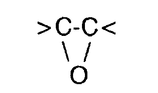
- the terminal-supporting plate or the covering case consists of a polyphenylene sulphide (PPS) resin, characterised in that an epoxy group, is substituted on either the chain or terminal phenylene groups in the polyphenylene sulphide chains of the resin.
- PPS polyphenylene sulphide
- the sealing resin and either the terminal-supporting plate or the covering case can deal flexibly with the stress imposed by the sealing resin in the hardening process, thereby preventing the terminal-supporting plate from peeling off from the covering case when an external force is applied to the terminal-supporting plate.
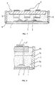
- Figure 1 shows an example of this invention, Figure 1 a being a sectional view, and Figure 1 b a partial external view of the terminal-supporting plate shown in Figure 1a.
- Figure 1 shows peripheral ridges 7a moulded on the outer peripheral edge surface of terminal-supporting plate 7, through which lead-out terminal 4 passes. The peripheral edge surface of the terminal-supporting plate 7 is thus roughened.
- These ridges 7a are produced either by being moulded together with the terminal-supporting plate or by grooving or slitting said plate.
- sealing resin 8 with which the inside of covering case 5 has been filled has run between the ridges 7a and hardened, the increase in the adhesive area and the anchoring effect by ridges 7a results in a high adhesive strength between terminal-supporting plate 7 and sealing resin 8. Accordingly, even when a large external force (e.g., tension or bending load) is applied to lead-out terminal 4 during actual operation, the bonding surface is no longer likely to peel off easily from terminal-supporting plate 7 or sealing resin 8.
- a large external force e.g., tension or bending load
- Figure 2 is a sectional view of a further development of the embodiment seen in Figure 1, in which irregular ridges 7a are moulded onto the outer peripheral surface of terminal-supporting plate 7 to roughen that surface, and a number of ridges 5b are moulded onto the inner surface of the wall of covering case 5 to roughen the inner surface of the wall.
- irregular ridges 7a are moulded onto the outer peripheral surface of terminal-supporting plate 7 to roughen that surface
- a number of ridges 5b are moulded onto the inner surface of the wall of covering case 5 to roughen the inner surface of the wall.
- uneven stepped sections 1 a and 5c are moulded.
- Roughening both the outer peripheral surface of terminal-supporting plate 7 and the inner wall of covering case 5 to obtain an uneven surface may be done using sandpaper or a cutting device of sufficient hardness compared with that of the resin to cut or scratch the outer peripheral surface of terminal-supporting plate 7 and the inner wall of covering case 5 after moulding.
- the cutting or scratching that is done after terminal-supporting plate 7 and covering case 5 are moulded also removes the mould lubricant present on their surfaces, the moulding resin and the sealing resin directly touch, thereby further enhancing adhesion.
- Figure 3 is a sectional view showing a further embodiment of this invention, in which the outer peripheral surface of terminal-supporting plate 7 is made to incline so as to face upwardly and the inclined surface is inclined face 7b where the angle a of the contact surface between the outer peripheral surface of terminal-supporting plate 7 and sealing resin 8 is greater than 0°, and the surface 5b of covering case 5 facing inclined face 7b is made to incline so as to face downwardly, the angle ⁇ of the contact surface between the surface 5b of covering case 5 facing inclined face 7b and sealing resin 8 is greater than 0°.
- Figure 4 is an enlarged sectional view showing another embodiment of this invention, in which a groove is formed in the section adhered to metallic base plate 1 and in the section adhered to covering case 5, and these grooves are fitted into each other to securely adhere these sections, and in which each of Figures 4a, 4b, and 4c shows an example of a different configuration.
- a groove 1b of width W 1 and depth L 1 is prepared in the peripheral section of metallic base plate 1;
- a groove 5e of width W 2 and depth L 2 is prepared in the end face of covering case 5, and 1 c indicates an outer wall bounding groove 1 b.
- the reference numbers 5f and 5g indicate the inner wall and outer wall, respectively, of groove 5e.
- the relationships between height L 3 and width W 3 of inner wall 5f of groove 5e, and depth L 1 and width W 1 of groove 1 b are such that L 3 > L 1 , and W 3 ⁇ W 1 , respectively. Furthermore, the relationship between the height of outer wall 5g of groove 5e (i.e. depth L 2 of groove 5e) and L 3 is that: L 2 > L 3 . Therefore, if the thickness of the metallic base plate 1 is t, the relationship between L 2 , L 3 , t, and L 1 can be defined as: L 2 ⁇ L 3 + t - L 1 , and the relationship between width W 4 of outer wall 1c of groove 1 b and width W 2 of groove 1 b is W 4 ⁇ W 2 .
- the tip of inner wall 5f can be fitted into groove 1b, and outer wall 1c can be fitted into groove 5e so as to interfit grooves 1 b and 5e. Then, the tip of inner wall 5f butts against the bottom of groove 1 b to form the vertical supporting section of covering case 5, and the tip of outer wall 5g does not extend as far as the lower surface of metallic base plate 1. Furthermore, a cavity exists in the bottom section of groove 5e.
- grooves 1b and 5e interfitted with each other When filling groove 1b with adhesive 6 and adhering metallic base plate 1 to covering case 5 with grooves 1 b and 5e interfitted with each other as stated above, they are made to adhere to each other over a wide adhesive area, and furthermore, since both grooves are interfitted with each other, metallic base plate 1 and covering case 5 will adhere strongly. In addition, since any surplus adhesive will remain in the cavity in the bottom section of groove 5e, the adhesive will not run outside the adhered section, nor for example, reach the lower surface of metallic base plate 1 to obstruct adhesion of the semiconductor device to an apparatus, and degrade the heat radiation of the device.
- Figure 4b shows a configuration where outer surface 5h of inner wall 5f of groove 5e of covering case 5 is roughened to further strengthen adhesion as compared to the embodiment of Figure 4a
- Figure 4c shows a configuration where the top section of groove 5e of the covering case is formed into taper 5i so that the adhesion area can be widened to enhance the adhesive strength and also make mould lubrication easier when moulding covering case 5.
- either the terminal-supporting plate or the covering case is made of straight-chain PPS resin, moulded using PPS resin of molecular structure containing the following group:
- Straight-chain PPS resin is a polycondensation of dichlorobenzene and sodium sulphide (Na-S-Na), which produces PPS with high molecular weight and which cleans the PPS with high molecular weight to remove impurity product NaCI therefrom.
- the aforementioned group is introduced or added to the addition group or terminal group of a molecular design to produce a PPS resin containing the group. Furthermore, during polycondensation, it is effective to mix the group together with an additive.
- FIG. 7 is a diagram of the molecular structure of PPS
- Figure 7a the molecular structure of an ordinary PPS polymer
- Figure 7b the molecular structure of the PPS resin relating to this invention, wherein the chain of the structure shown in Figure 7a is cut at the middle, and wherein a molecular structure having the following group is added to part of a and b, c, d, and e of a benzene ring:
- straight-chain PPS that contains the group, not only can the heat resistance (260°C), flame resistance (the self-quenching property of PPS resin is industrially advantageous), and range of colours (black; green; white), which are the main characteristics of straight-chain PPS resin, be reproduced, but also an effect can be obtained that the group is connected by means of hydrogen bonding (X-H ... Y or X ... H-Y) to the same group of epoxy resin, that PPS resin and epoxy resin are bonded at a molecular level, and that adhesion of the terminal-supporting plate to the covering case becomes stronger.
- fibreglass or silica (SiO 2 ) is preferable for enhancing the mechanical strength of the resin and the adhesion of PPS resin to epoxy resin.
- this invention has the following effects.
Landscapes
- Structures Or Materials For Encapsulating Or Coating Semiconductor Devices Or Solid State Devices (AREA)
Description
- This invention relates to a resin-sealed semiconductor device, and particularly relates to a resin-sealed transistor module.
- Figure 5 shows a conventional resin-sealed semiconductor device. In this diagram,
reference number 1 designates a metallic base plate that also serves as a heat radiation plate, reference number 2 a semiconductor element that is mounted onmetallic base plate 1 viasubstrate 3, reference number 4 a lead-out terminal soldered to the surface electrode ofsemiconductor element 2 or to the conductor pattern ofsubstrate 3 and drawn out upwardly.Reference number 5 indicates a moulded resin covering case bonded with adhesive 6 to the peripheral edge of themetallic base plate 1, and a moulded resin terminal-supportingplate 7 serves as the case lid on the upper surface of coveringcase 5. A sealingresin 8 fills the inside of coveringcase 5. In addition, there are also two different types of sealing resin 8: one is made entirely of epoxy resin, and the other is divided into two layers (upper and lower), wherein the lower layer is made of silicon gel and the upper layer is made of epoxy resin. In the two-layered (upper and lower) sealingresin 8, as the cross-sectional view of Figure 6 shows, astep 5a is usually formed on the inner surface of coveringcase 5, and filling the inside of coveringcase 5 withsilicon gel 8a stops before the level ofsilicon gel 8a reaches thestep 5a. The remaining portion is filled withepoxy resin 8b to harden the inside of coveringcase 5. A device of this type is known from JP-A-4206554. - Although the type of resin material for covering
case 5 and terminal-supportingplate 7 are selected in consideration of their resistance to heat, flameproofing property, colouring property, electrical characteristics, and moulding costs, usually PBT (polybutylene terephthalate) resin or PPS (polyphenylene sulphide) resin is used for coveringcase 5 and PPS resin for terminal-supportingplate 7. - According to the configuration of said conventional resin-sealed semiconductor device, peeling occurs in between the components during actual use or in temperature cycle tests by mutual adhesive failure. This peeling further causes problems such as degrading of moisture resistance performance of the device and leaking of the sealing resin (gelatinoid filler) from the covering case. In particular, the adherent surface between the covering case and the sealing resin, and the adherent surface between the terminal-supporting plate and the sealing resin easily separate. Epoxy resin is used as the sealing resin and solidified at about 135°C. The transition temperature required to solidify epoxy resin into glass is 140 - 160°C, and at temperatures below that range the elasticity of the hardened epoxy resin is highly stable at approximately 1,200 kg/mm2. The glass transition temperature for PPS resin is 80 - 90°C, and although at temperatures below this range the elasticity of PPS resin is very stable at approximately about 1,800 kg/mm2, at temperatures above this range the elasticity of the PPS resin tends gradually to decrease. Accordingly, for a covering case and terminal-supporting plate made of PPS resin, in order to fill the inside of the covering case and solidify the PPS resin at about 135°C, since the elasticity of the PPS resin, which decreases somewhat, does not change considerably, a difference in the elasticity of the PPS resin and the epoxy resins arises, causing further latent stress in the adherent surface between the covering case and the sealing resin, and between the terminal-supporting plate and the sealing resin. Since an external mechanical stress such as high tension or bending load is likely to be applied to said adherent surfaces during connection of the external wiring to lead-out terminals, peeling can occur not only between the terminal-supporting plate which supports the lead-out terminals and the sealing resin, but also between the covering case and the sealing resin. When the lead-out terminal comes loose due to the peeling thus caused, stress is also applied to the soldered sections between the lead-out terminals and the semiconductor device, thereby causing serious defects such as damage to the semiconductor device.
- Furthermore, when an attempt is made to use an adhesive to solidify the adhesive used to bond the metallic base plate to the external covering case, the adhesive runs out of the adherent section and then under the lower surface of the metallic base plate and adheres thereto, thereby damaging the smoothness of the mounting surface, reducing the adhesiveness of the semiconductor device to an apparatus, degrading the heat radiation performance of the semiconductor device or causing the adhesive to further run into screw holes prepared on the metallic base plate for mounting the semiconductor device, thereby preventing the mounting of the semiconductor device or loosening the screws in use.
- JP-A-04 198 267 proposes the use of resin compositions comprising a mixture of polyarylene sulphide resins and carboxyl containing polyarylene sulphide resins for moulding electronic parts as the mixture has improved adhesive properties.
- The object of the present invention is to provide stiff and highly reliable resin-sealed semiconductor devices by resolving said problems and by preventing the adhesive between structural components from losing its adhesive properties.
- According to the invention there is provided a resin-sealed semiconductor device wherein the terminal-supporting plate or the covering case consists of a polyphenylene sulphide (PPS) resin, characterised in that an epoxy group,is substituted on either the chain or terminal phenylene groups in the polyphenylene sulphide chains of the resin.

- Accordingly, the sealing resin and either the terminal-supporting plate or the covering case can deal flexibly with the stress imposed by the sealing resin in the hardening process, thereby preventing the terminal-supporting plate from peeling off from the covering case when an external force is applied to the terminal-supporting plate.
- An exemplary embodiment of this invention is explained below with reference to the attached drawings, in which:
- Figure 1 shows a first embodiment of the present device, wherein Figure 1a is a sectional view, and Figure 1b is a partial external view of the terminal-supporting plate shown in Figure 1a;
- Figure 2 is a sectional view showing a second embodiment of the device of this invention;
- Figure 3 is a sectional view showing a third embodiment of the present device;
- Figure 4 is a sectional view showing a fourth embodiment of the present device;
- Figure 5 is a sectional view of a conventional resin-sealed semiconductor device;
- Figure 6 is a sectional view of a second conventional resin-sealed semiconductor device; and
- Figure 7 is a diagram showing the molecular structure of PPS resin, wherein Figure 7a shows the structure of an ordinary PPS polymer, wherein Figure 7b shows the structure of the PPS polymer related to this invention.
-
- In the drawings, components which correspond to components shown in Figures 5 and 6 are designated by the same reference numbers.
- Figure 1 shows an example of this invention, Figure 1 a being a sectional view, and Figure 1 b a partial external view of the terminal-supporting plate shown in Figure 1a. Figure 1 shows
peripheral ridges 7a moulded on the outer peripheral edge surface of terminal-supportingplate 7, through which lead-outterminal 4 passes. The peripheral edge surface of the terminal-supportingplate 7 is thus roughened. Theseridges 7a are produced either by being moulded together with the terminal-supporting plate or by grooving or slitting said plate. - In the above configuration, since sealing
resin 8 with which the inside of coveringcase 5 has been filled has run between theridges 7a and hardened, the increase in the adhesive area and the anchoring effect byridges 7a results in a high adhesive strength between terminal-supportingplate 7 and sealingresin 8. Accordingly, even when a large external force (e.g., tension or bending load) is applied to lead-outterminal 4 during actual operation, the bonding surface is no longer likely to peel off easily from terminal-supportingplate 7 or sealingresin 8. - Figure 2 is a sectional view of a further development of the embodiment seen in Figure 1, in which
irregular ridges 7a are moulded onto the outer peripheral surface of terminal-supportingplate 7 to roughen that surface, and a number ofridges 5b are moulded onto the inner surface of the wall of coveringcase 5 to roughen the inner surface of the wall. Onto the adherent surface provided for adhesive 6 betweenmetallic base plate 1 and coveringcase 5, uneven steppedsections 1 a and 5c are moulded. With the above configuration, both the adhesive strength between coveringcase 5 and sealingresin 8, and that betweenmetallic base plate 1 and coveringcase 5 are enhanced, thereby increasing the adhesive strength of the entire resin-sealed semiconductor device. Roughening both the outer peripheral surface of terminal-supportingplate 7 and the inner wall of coveringcase 5 to obtain an uneven surface may be done using sandpaper or a cutting device of sufficient hardness compared with that of the resin to cut or scratch the outer peripheral surface of terminal-supportingplate 7 and the inner wall of coveringcase 5 after moulding. In this case, since the cutting or scratching that is done after terminal-supportingplate 7 and coveringcase 5 are moulded also removes the mould lubricant present on their surfaces, the moulding resin and the sealing resin directly touch, thereby further enhancing adhesion. - Figure 3 is a sectional view showing a further embodiment of this invention, in which the outer peripheral surface of terminal-supporting
plate 7 is made to incline so as to face upwardly and the inclined surface is inclined face 7b where the angle a of the contact surface between the outer peripheral surface of terminal-supportingplate 7 and sealingresin 8 is greater than 0°, and thesurface 5b of coveringcase 5 facing inclined face 7b is made to incline so as to face downwardly, the angle β of the contact surface between thesurface 5b of coveringcase 5 facing inclined face 7b and sealingresin 8 is greater than 0°. Inclining the contact surface between the outer peripheral surface of terminal-supportingplate 7 and sealingresin 8 and that part of the contact surface between the surface of coveringcase 5 facing the former inclined surface, and sealingresin 8 will prevent terminal-supportingplate 7 from slipping when an external force is applied to lead-outterminal 4. Although such an effect can be obtained also by inclining only the outer peripheral surface of terminal-supportingplate 7, it is found that by also inclining the part of the surface of coveringcase 5 facing the slanting surface, the effect of protecting terminal-supportingplate 7 from slipping is improved. The above inclination can be achieved by changing the moulding die or by cutting after moulding. Furthermore, unevenly finishing these slanting surfaces is the most preferred method to obtain the aforementioned roughening effect. - Figure 4 is an enlarged sectional view showing another embodiment of this invention, in which a groove is formed in the section adhered to
metallic base plate 1 and in the section adhered to coveringcase 5, and these grooves are fitted into each other to securely adhere these sections, and in which each of Figures 4a, 4b, and 4c shows an example of a different configuration. In Figure 4a, a groove 1b of width W1 and depth L1 is prepared in the peripheral section ofmetallic base plate 1; agroove 5e of width W2 and depth L2 is prepared in the end face of coveringcase reference numbers groove 5e. In terms of physical dimensions, the relationships between height L3 and width W3 ofinner wall 5f ofgroove 5e, and depth L1 and width W1 of groove 1 b are such that L3 > L1, and W3 < W1, respectively. Furthermore, the relationship between the height ofouter wall 5g ofgroove 5e (i.e. depth L2 ofgroove 5e) and L3 is that: L2 > L3. Therefore, if the thickness of themetallic base plate 1 is t, the relationship between L2, L3, t, and L1 can be defined as: L2 < L3 + t - L1, and the relationship between width W4 ofouter wall 1c of groove 1 b and width W2 of groove 1 b is W4 < W2. Accordingly, when adheringmetallic base plate 1 to coveringcase 5, the tip ofinner wall 5f can be fitted into groove 1b, andouter wall 1c can be fitted intogroove 5e so as to interfitgrooves 1 b and 5e. Then, the tip ofinner wall 5f butts against the bottom of groove 1 b to form the vertical supporting section of coveringcase 5, and the tip ofouter wall 5g does not extend as far as the lower surface ofmetallic base plate 1. Furthermore, a cavity exists in the bottom section ofgroove 5e. When filling groove 1b with adhesive 6 and adheringmetallic base plate 1 to coveringcase 5 withgrooves 1 b and 5e interfitted with each other as stated above, they are made to adhere to each other over a wide adhesive area, and furthermore, since both grooves are interfitted with each other,metallic base plate 1 and coveringcase 5 will adhere strongly. In addition, since any surplus adhesive will remain in the cavity in the bottom section ofgroove 5e, the adhesive will not run outside the adhered section, nor for example, reach the lower surface ofmetallic base plate 1 to obstruct adhesion of the semiconductor device to an apparatus, and degrade the heat radiation of the device. - Figure 4b shows a configuration where
outer surface 5h ofinner wall 5f ofgroove 5e of coveringcase 5 is roughened to further strengthen adhesion as compared to the embodiment of Figure 4a, and Figure 4c shows a configuration where the top section ofgroove 5e of the covering case is formed intotaper 5i so that the adhesion area can be widened to enhance the adhesive strength and also make mould lubrication easier when moulding coveringcase 5. - In this invention, either the terminal-supporting plate or the covering case is made of straight-chain PPS resin, moulded using PPS resin of molecular structure containing the following group:Straight-chain PPS resin is a polycondensation of dichlorobenzene
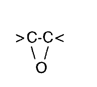 and sodium sulphide (Na-S-Na), which produces PPS with high molecular weight and which cleans the PPS with high molecular weight to remove impurity product NaCI therefrom. Then, the aforementioned group is introduced or added to the addition group or terminal group of a molecular design to produce a PPS resin containing the group. Furthermore, during polycondensation, it is effective to mix the group together with an additive. It is also effective to use ordinary PPS resin to mould the terminal-supporting plate and the covering case, and then apply ultraviolet light of wavelength 185 nm or 254 nm to the contact surfaces between the terminal-supporting plate, covering case, and sealing resin, or to apply plasma thereto to generate a radical on the surface. Figure 7 is a diagram of the molecular structure of PPS, Figure 7a the molecular structure of an ordinary PPS polymer, and Figure 7b the molecular structure of the PPS resin relating to this invention, wherein the chain of the structure shown in Figure 7a is cut at the middle, and wherein a molecular structure having the following group is added to part of a and b, c, d, and e of a benzene ring:

- As mentioned above, by forming straight-chain PPS that contains the group, not only can the heat resistance (260°C), flame resistance (the self-quenching property of PPS resin is industrially advantageous), and range of colours (black; green; white), which are the main characteristics of straight-chain PPS resin, be reproduced, but also an effect can be obtained that the group is connected by means of hydrogen bonding (X-H ... Y or X ... H-Y) to the same group of epoxy resin, that PPS resin and epoxy resin are bonded at a molecular level, and that adhesion of the terminal-supporting plate to the covering case becomes stronger.
- Furthermore, adding fibreglass or silica (SiO2) to the above PPS resin is preferable for enhancing the mechanical strength of the resin and the adhesion of PPS resin to epoxy resin.
- Although the aforementioned has been described separately for the covering case and the terminal-supporting plate, making PPS resin that contains at least the aforementioned group is effective even for a monolithic mould of the covering case and the terminal-supporting plate.
- In accordance with the characteristics mentioned above, this invention has the following effects.
- By moulding either the terminal-supporting plate or the covering case with PPS resin prepared by combining agroup with part of either the addition group or terminal group of a molecular design, bonding at molecular level is further added to the adhesion of the terminal-supporting plate or the covering case and sealing resin, thereby improving the strength of the adhesion.
Claims (1)
- A resin-sealed semiconductor device wherein the terminal-supporting plate (7) or the covering case (5) consists of a polyphenylene sulphide (PPS) resin, characterised in that an epoxy group,is substituted on either the chain or terminal phenylene groups in the polyphenylene sulphide chains of the resin.

Applications Claiming Priority (7)
| Application Number | Priority Date | Filing Date | Title |
|---|---|---|---|
| JP364693 | 1993-01-13 | ||
| JP364693 | 1993-01-13 | ||
| JP3646/93 | 1993-01-13 | ||
| JP5104849A JPH06268102A (en) | 1993-01-13 | 1993-05-06 | Resin-sealed semiconductor device |
| JP10484993 | 1993-05-06 | ||
| JP104849/93 | 1993-05-06 | ||
| EP94300096A EP0608051B1 (en) | 1993-01-13 | 1994-01-07 | Resin-sealed semiconductor device |
Related Parent Applications (2)
| Application Number | Title | Priority Date | Filing Date |
|---|---|---|---|
| EP94300096A Division EP0608051B1 (en) | 1993-01-13 | 1994-01-07 | Resin-sealed semiconductor device |
| EP94300096.8 Division | 1994-01-07 |
Publications (3)
| Publication Number | Publication Date |
|---|---|
| EP0749159A2 EP0749159A2 (en) | 1996-12-18 |
| EP0749159A3 EP0749159A3 (en) | 1997-04-02 |
| EP0749159B1 true EP0749159B1 (en) | 2001-08-16 |
Family
ID=26337276
Family Applications (2)
| Application Number | Title | Priority Date | Filing Date |
|---|---|---|---|
| EP94300096A Expired - Lifetime EP0608051B1 (en) | 1993-01-13 | 1994-01-07 | Resin-sealed semiconductor device |
| EP96114416A Expired - Lifetime EP0749159B1 (en) | 1993-01-13 | 1994-01-07 | Resin-sealed semiconductor device |
Family Applications Before (1)
| Application Number | Title | Priority Date | Filing Date |
|---|---|---|---|
| EP94300096A Expired - Lifetime EP0608051B1 (en) | 1993-01-13 | 1994-01-07 | Resin-sealed semiconductor device |
Country Status (4)
| Country | Link |
|---|---|
| US (1) | US5606200A (en) |
| EP (2) | EP0608051B1 (en) |
| JP (1) | JPH06268102A (en) |
| DE (2) | DE69407064T2 (en) |
Families Citing this family (32)
| Publication number | Priority date | Publication date | Assignee | Title |
|---|---|---|---|---|
| JP3201187B2 (en) * | 1994-12-08 | 2001-08-20 | 富士電機株式会社 | Semiconductor device |
| DE19649798A1 (en) * | 1996-12-02 | 1998-06-04 | Abb Research Ltd | Power semiconductor module |
| CN1146988C (en) * | 1997-12-08 | 2004-04-21 | 东芝株式会社 | Package for semiconductor power device and method for assembling the same |
| US6184464B1 (en) * | 1998-04-27 | 2001-02-06 | Square D Company | Protective containment apparatus for potted electronic circuits |
| US6222263B1 (en) * | 1999-10-19 | 2001-04-24 | International Business Machines Corporation | Chip assembly with load-bearing lid in thermal contact with the chip |
| JP4623987B2 (en) * | 2003-06-27 | 2011-02-02 | 京セラ株式会社 | Capacitor and its mounting structure |
| EP2750187B1 (en) * | 2011-08-25 | 2020-01-01 | Fuji Electric Co., Ltd. | Semiconductor device and semiconductor device manufacturing method |
| DE102012211446B4 (en) * | 2012-07-02 | 2016-05-12 | Infineon Technologies Ag | EXPLOSION-PROTECTED SEMICONDUCTOR MODULE |
| KR101543100B1 (en) * | 2013-12-02 | 2015-08-07 | 현대자동차주식회사 | Controller intergrated fuel pump module |
| JP6451257B2 (en) * | 2014-11-21 | 2019-01-16 | 富士電機株式会社 | Semiconductor device |
| CN108292631B (en) * | 2015-12-04 | 2021-08-06 | 三菱电机株式会社 | semiconductor module |
| JP6081042B1 (en) * | 2015-12-16 | 2017-02-15 | 三菱電機株式会社 | Semiconductor device and manufacturing method thereof |
| WO2017104159A1 (en) * | 2015-12-16 | 2017-06-22 | 三菱電機株式会社 | Semiconductor device and method for manufacturing same |
| DE102016202600A1 (en) * | 2016-02-19 | 2017-08-24 | Siemens Aktiengesellschaft | Electric module with electrical component |
| JP6699742B2 (en) * | 2016-09-20 | 2020-05-27 | 三菱電機株式会社 | Semiconductor device |
| WO2018207656A1 (en) * | 2017-05-11 | 2018-11-15 | 三菱電機株式会社 | Power module, electric power conversion device, and method for producing power module |
| US11227808B2 (en) | 2017-09-05 | 2022-01-18 | Mitsubishi Electric Corporation | Power module and method for fabricating the same, and power conversion device |
| DE112018004816T5 (en) * | 2017-09-05 | 2020-06-10 | Mitsubishi Electric Corporation | PERFORMANCE MODULE, METHOD FOR PRODUCING THE SAME AND PERFORMANCE CONVERTER |
| JP7045975B2 (en) | 2018-11-20 | 2022-04-01 | 三菱電機株式会社 | Semiconductor devices and their manufacturing methods, as well as power conversion devices |
| US11935799B2 (en) * | 2019-06-25 | 2024-03-19 | Intel Corporation | Integrated circuit package lids with polymer features |
| JP7173375B2 (en) * | 2019-11-27 | 2022-11-16 | 三菱電機株式会社 | semiconductor module |
| JP7247124B2 (en) | 2020-01-07 | 2023-03-28 | 三菱電機株式会社 | semiconductor module |
| JP2021111669A (en) * | 2020-01-08 | 2021-08-02 | 三菱電機株式会社 | Semiconductor device and electric power conversion system |
| DE112020006549T5 (en) * | 2020-01-17 | 2022-11-03 | Mitsubishi Electric Corporation | POWER MODULE AND POWER CONVERTER |
| JP2021132080A (en) * | 2020-02-18 | 2021-09-09 | 富士電機株式会社 | Semiconductor device |
| JP7559432B2 (en) * | 2020-08-27 | 2024-10-02 | 富士電機株式会社 | Semiconductor module and method for manufacturing the same |
| JP7647388B2 (en) * | 2021-06-25 | 2025-03-18 | 富士電機株式会社 | Semiconductor Module |
| JP7637852B2 (en) * | 2021-07-07 | 2025-03-03 | 三菱電機株式会社 | Semiconductor device and inverter device |
| JP2023061442A (en) * | 2021-10-20 | 2023-05-02 | 富士電機株式会社 | Semiconductor device and method for manufacturing semiconductor device |
| JP2023114084A (en) * | 2022-02-04 | 2023-08-17 | 富士電機株式会社 | Semiconductor device and method for manufacturing semiconductor device |
| JP2024045842A (en) * | 2022-09-22 | 2024-04-03 | キオクシア株式会社 | Semiconductor device and semiconductor device manufacturing method |
| CN117198901B (en) * | 2023-11-07 | 2024-01-23 | 通富微电子股份有限公司 | Power module packaging method and power module |
Family Cites Families (15)
| Publication number | Priority date | Publication date | Assignee | Title |
|---|---|---|---|---|
| JPS60119759A (en) * | 1983-11-30 | 1985-06-27 | Mitsubishi Electric Corp | Semiconductor device |
| JPS60254350A (en) * | 1984-05-31 | 1985-12-16 | Nec Ic Microcomput Syst Ltd | Data communication control device |
| JPS60254643A (en) * | 1984-05-31 | 1985-12-16 | Toshiba Corp | Resin-sealed semiconductor device |
| JPS61148845A (en) * | 1984-12-21 | 1986-07-07 | Mitsubishi Electric Corp | Semiconductor device |
| JPS63164245A (en) * | 1986-12-26 | 1988-07-07 | Hitachi Ltd | Electronic component |
| JPS63219145A (en) * | 1987-03-09 | 1988-09-12 | Sumitomo Bakelite Co Ltd | Pps sealed electronic component |
| JPH0834271B2 (en) * | 1987-03-09 | 1996-03-29 | 住友ベークライト株式会社 | PPS sealed electronic parts |
| JPH0428764A (en) * | 1990-05-24 | 1992-01-31 | Sumitomo Bakelite Co Ltd | Polyphenylene sulfide resin composition |
| US5243217A (en) * | 1990-11-03 | 1993-09-07 | Fuji Electric Co., Ltd. | Sealed semiconductor device with protruding portion |
| JPH04198267A (en) * | 1990-11-27 | 1992-07-17 | Dainippon Ink & Chem Inc | Polyarylene sufide resin composition |
| JPH04206554A (en) * | 1990-11-30 | 1992-07-28 | Hitachi Ltd | Semiconductor device |
| JP2867753B2 (en) * | 1991-02-25 | 1999-03-10 | 富士電機株式会社 | Semiconductor device |
| JPH04274350A (en) * | 1991-03-01 | 1992-09-30 | Fuji Electric Co Ltd | semiconductor equipment |
| JP2642548B2 (en) * | 1991-09-26 | 1997-08-20 | 株式会社東芝 | Semiconductor device and manufacturing method thereof |
| JP2936855B2 (en) * | 1991-12-26 | 1999-08-23 | 富士電機株式会社 | Power semiconductor device |
-
1993
- 1993-05-06 JP JP5104849A patent/JPH06268102A/en active Pending
-
1994
- 1994-01-07 DE DE69407064T patent/DE69407064T2/en not_active Expired - Lifetime
- 1994-01-07 EP EP94300096A patent/EP0608051B1/en not_active Expired - Lifetime
- 1994-01-07 EP EP96114416A patent/EP0749159B1/en not_active Expired - Lifetime
- 1994-01-07 DE DE69427995T patent/DE69427995T2/en not_active Expired - Lifetime
- 1994-01-12 US US08/180,481 patent/US5606200A/en not_active Expired - Lifetime
Also Published As
| Publication number | Publication date |
|---|---|
| DE69427995T2 (en) | 2001-11-29 |
| US5606200A (en) | 1997-02-25 |
| JPH06268102A (en) | 1994-09-22 |
| EP0749159A3 (en) | 1997-04-02 |
| DE69427995D1 (en) | 2001-09-20 |
| EP0749159A2 (en) | 1996-12-18 |
| EP0608051A3 (en) | 1994-09-21 |
| EP0608051B1 (en) | 1997-12-03 |
| EP0608051A2 (en) | 1994-07-27 |
| DE69407064T2 (en) | 1998-06-04 |
| DE69407064D1 (en) | 1998-01-15 |
Similar Documents
| Publication | Publication Date | Title |
|---|---|---|
| EP0749159A2 (en) | Resin-sealed semiconductor device | |
| US6861683B2 (en) | Optoelectronic component using two encapsulating materials and the method of making the same | |
| US7723162B2 (en) | Method for producing shock and tamper resistant microelectronic devices | |
| US6126885A (en) | Method for manufacturing resin-molded semiconductor device | |
| US5851847A (en) | Photonic device and process for fabricating the same | |
| KR20030039553A (en) | Wire bonding pad structure of semiconductor package pcb | |
| CN101814481B (en) | No-pad lead frame structure and production method thereof | |
| KR19990062872A (en) | Package for semiconductor power device and assembly method thereof | |
| JP3362219B2 (en) | Manufacturing method of hermetically sealed package | |
| EP0645812B1 (en) | Resin-sealed semiconductor device | |
| EP0892427B1 (en) | Method of sealing electronic parts with a resin | |
| EP0307946B1 (en) | Method of manufacturing a resin insulated type semiconductor device | |
| US6090237A (en) | Apparatus for restraining adhesive overflow in a multilayer substrate assembly during lamination | |
| EP0971009B1 (en) | Adhesive composition for bonding semiconductor chips | |
| CN1324699C (en) | Power semiconductor module | |
| US7432601B2 (en) | Semiconductor package and fabrication process thereof | |
| US20110057330A1 (en) | Electronic device and method of manufacturing electronic device | |
| JP4029278B2 (en) | Semiconductor device and manufacturing method thereof | |
| US20020079438A1 (en) | Image sensor package and substrate thereof | |
| JP2003163380A (en) | Optical semiconductor device and method of manufacturing the same | |
| JP2825387B2 (en) | Light emitting element | |
| JP4336407B2 (en) | Circuit board | |
| JP4813683B2 (en) | Resin molded circuit device | |
| KR100804509B1 (en) | Dummy for cleaning of semiconductor mold mold | |
| EP0670595A1 (en) | Resin-sealed semiconductor device |
Legal Events
| Date | Code | Title | Description |
|---|---|---|---|
| PUAI | Public reference made under article 153(3) epc to a published international application that has entered the european phase |
Free format text: ORIGINAL CODE: 0009012 |
|
| 17P | Request for examination filed |
Effective date: 19960909 |
|
| AC | Divisional application: reference to earlier application |
Ref document number: 608051 Country of ref document: EP |
|
| AK | Designated contracting states |
Kind code of ref document: A2 Designated state(s): DE FR GB |
|
| PUAL | Search report despatched |
Free format text: ORIGINAL CODE: 0009013 |
|
| AK | Designated contracting states |
Kind code of ref document: A3 Designated state(s): DE FR GB |
|
| 17Q | First examination report despatched |
Effective date: 19990305 |
|
| GRAG | Despatch of communication of intention to grant |
Free format text: ORIGINAL CODE: EPIDOS AGRA |
|
| GRAG | Despatch of communication of intention to grant |
Free format text: ORIGINAL CODE: EPIDOS AGRA |
|
| GRAH | Despatch of communication of intention to grant a patent |
Free format text: ORIGINAL CODE: EPIDOS IGRA |
|
| GRAH | Despatch of communication of intention to grant a patent |
Free format text: ORIGINAL CODE: EPIDOS IGRA |
|
| GRAA | (expected) grant |
Free format text: ORIGINAL CODE: 0009210 |
|
| AC | Divisional application: reference to earlier application |
Ref document number: 608051 Country of ref document: EP |
|
| AK | Designated contracting states |
Kind code of ref document: B1 Designated state(s): DE FR GB |
|
| REF | Corresponds to: |
Ref document number: 69427995 Country of ref document: DE Date of ref document: 20010920 |
|
| ET | Fr: translation filed | ||
| REG | Reference to a national code |
Ref country code: GB Ref legal event code: IF02 |
|
| PLBE | No opposition filed within time limit |
Free format text: ORIGINAL CODE: 0009261 |
|
| STAA | Information on the status of an ep patent application or granted ep patent |
Free format text: STATUS: NO OPPOSITION FILED WITHIN TIME LIMIT |
|
| 26N | No opposition filed | ||
| REG | Reference to a national code |
Ref country code: GB Ref legal event code: 746 Effective date: 20070115 |
|
| REG | Reference to a national code |
Ref country code: GB Ref legal event code: 732E Free format text: REGISTERED BETWEEN 20100401 AND 20100407 |
|
| PGFP | Annual fee paid to national office [announced via postgrant information from national office to epo] |
Ref country code: FR Payment date: 20100208 Year of fee payment: 17 |
|
| REG | Reference to a national code |
Ref country code: FR Ref legal event code: TP Ref country code: FR Ref legal event code: CD |
|
| PGFP | Annual fee paid to national office [announced via postgrant information from national office to epo] |
Ref country code: GB Payment date: 20100106 Year of fee payment: 17 Ref country code: DE Payment date: 20091231 Year of fee payment: 17 |
|
| GBPC | Gb: european patent ceased through non-payment of renewal fee |
Effective date: 20110107 |
|
| REG | Reference to a national code |
Ref country code: FR Ref legal event code: ST Effective date: 20110930 |
|
| PG25 | Lapsed in a contracting state [announced via postgrant information from national office to epo] |
Ref country code: FR Free format text: LAPSE BECAUSE OF NON-PAYMENT OF DUE FEES Effective date: 20110131 |
|
| PG25 | Lapsed in a contracting state [announced via postgrant information from national office to epo] |
Ref country code: GB Free format text: LAPSE BECAUSE OF NON-PAYMENT OF DUE FEES Effective date: 20110107 |
|
| REG | Reference to a national code |
Ref country code: DE Ref legal event code: R119 Ref document number: 69427995 Country of ref document: DE Effective date: 20110802 |
|
| PG25 | Lapsed in a contracting state [announced via postgrant information from national office to epo] |
Ref country code: DE Free format text: LAPSE BECAUSE OF NON-PAYMENT OF DUE FEES Effective date: 20110802 |