EP0744754B1 - Verfahren und Vorrichtung für Injektion von heissen Ladungsträgern - Google Patents
Verfahren und Vorrichtung für Injektion von heissen Ladungsträgern Download PDFInfo
- Publication number
- EP0744754B1 EP0744754B1 EP96303419A EP96303419A EP0744754B1 EP 0744754 B1 EP0744754 B1 EP 0744754B1 EP 96303419 A EP96303419 A EP 96303419A EP 96303419 A EP96303419 A EP 96303419A EP 0744754 B1 EP0744754 B1 EP 0744754B1
- Authority
- EP
- European Patent Office
- Prior art keywords
- volts
- drain
- source
- substrate
- voltage
- Prior art date
- Legal status (The legal status is an assumption and is not a legal conclusion. Google has not performed a legal analysis and makes no representation as to the accuracy of the status listed.)
- Expired - Lifetime
Links
Images


Classifications
-
- H—ELECTRICITY
- H10—SEMICONDUCTOR DEVICES; ELECTRIC SOLID-STATE DEVICES NOT OTHERWISE PROVIDED FOR
- H10B—ELECTRONIC MEMORY DEVICES
- H10B69/00—Erasable-and-programmable ROM [EPROM] devices not provided for in groups H10B41/00 - H10B63/00, e.g. ultraviolet erasable-and-programmable ROM [UVEPROM] devices
-
- G—PHYSICS
- G11—INFORMATION STORAGE
- G11C—STATIC STORES
- G11C16/00—Erasable programmable read-only memories
- G11C16/02—Erasable programmable read-only memories electrically programmable
- G11C16/06—Auxiliary circuits, e.g. for writing into memory
- G11C16/34—Determination of programming status, e.g. threshold voltage, overprogramming or underprogramming, retention
- G11C16/3404—Convergence or correction of memory cell threshold voltages; Repair or recovery of overerased or overprogrammed cells
- G11C16/3409—Circuits or methods to recover overerased nonvolatile memory cells detected during erase verification, usually by means of a "soft" programming step
-
- G—PHYSICS
- G11—INFORMATION STORAGE
- G11C—STATIC STORES
- G11C16/00—Erasable programmable read-only memories
- G11C16/02—Erasable programmable read-only memories electrically programmable
- G11C16/06—Auxiliary circuits, e.g. for writing into memory
- G11C16/10—Programming or data input circuits
-
- G—PHYSICS
- G11—INFORMATION STORAGE
- G11C—STATIC STORES
- G11C16/00—Erasable programmable read-only memories
- G11C16/02—Erasable programmable read-only memories electrically programmable
- G11C16/06—Auxiliary circuits, e.g. for writing into memory
- G11C16/10—Programming or data input circuits
- G11C16/12—Programming voltage switching circuits
-
- G—PHYSICS
- G11—INFORMATION STORAGE
- G11C—STATIC STORES
- G11C16/00—Erasable programmable read-only memories
- G11C16/02—Erasable programmable read-only memories electrically programmable
- G11C16/06—Auxiliary circuits, e.g. for writing into memory
- G11C16/34—Determination of programming status, e.g. threshold voltage, overprogramming or underprogramming, retention
- G11C16/3404—Convergence or correction of memory cell threshold voltages; Repair or recovery of overerased or overprogrammed cells
Definitions
- the invention is directed to electrically programmable read-only memory (EPROMs and EEPROMs) devices.
- a nonvolatile memory is a type of memory that retains stored data when power is removed.
- nonvolatile memories including read only memories (ROMs), programmable read only memories (PROMs), erasable programmable read only memories (EPROMs), and electrically erasable programmable read only memories (EEPROMs).
- ROMs read only memories
- PROMs programmable read only memories
- EPROMs erasable programmable read only memories
- EEPROMs electrically erasable programmable read only memories
- An EEPROM is erased using ultraviolet light and an EEPROM is erased using an electrical signal. An electrical signal is used to write EPROMS and EEPROMS.
- flash EEPROM flash indicating all memory cells or sectors of cells can be erased at once
- memory cells are simultaneously erased to a low threshold voltage and then programmed, either individually or in small groups, to a high threshold voltage.
- EPROMs and EEPROMs are commonly used in data processing systems that require a nonvolatile
- a typical device structure for EPROMS is the floating-gate polysilicon transistor.
- a typical floating gate structure is illustrated in FIG. 1.
- a floating gate 10 sandwiched between two insulator layers 20 and 60, is between the substrate 30 and the ordinary select-gate electrode 40.
- the structure depicted in FIG. 1 is a stacked gate memory cell, the word stacked indicating that the floating gate 10 is stacked over the source 50 and drain 70 portions of the substrate.
- Another EPROM structure is a split gate structure wherein the portion of the floating gate only overlies the drain and no portion of the floating gate overlies the source.
- Split gate EPROM device structures are described in U.S. Patent No. 5,349,220, to Hong. As a result, in EPROMS, the select-gate voltage must be capacitively coupled in series with the floating gate rather than directly to the underlying channel.
- n-channel and p-channel devices with the above structures.
- the source and drain are doped with an n-type dopant and the substrate is doped with a p-type dopant.
- the source and drain contain p-type dopant and the substrate contains n-type dopant.
- silicon based substrates such as silicon or silicon-germanium (SiGe) alloys
- an example of a p-type dopant is boron and examples of suitable n-type dopants are arsenic and phosphorous.
- EPROMS are programmed by applying a set of bias voltages to the device depicted in FIG. 1.
- the voltage applied to the select-gate (hereinafter referred to as a control gate) is V C .
- the voltage applied to the drain is V D
- the voltage applied to the source is V S .
- writing biases are used to introduce additional negative charge onto the floating gate, thereby writing the cell. However, if the charged state is chosen as the "unwritten" state, introducing additional negative charge onto the floating gate will erase the cell. Bias conditions that are used to introduce a more negatively charged state are different from bias conditions that are used to read the charged state or to create a more positively charged state.
- These write biases are typically a high control gate-to-source voltage (V CS ) and/or a high drain-to-source voltage (V DS ). These programming voltages are sufficient to cause a transfer of electrons from the bulk of the device (channel 80 and/or source 50 and/or drain 70) region to the floating gate 10 where they are trapped, thereby charging the floating gate more negatively. Charge is trapped in the floating gate 10 because the floating gate is isolated from the select-gate 40 by an insulating oxide layer 60 and from the drain-source-substrate region by another thin oxide insulating layer 20. The effect of trapping electrons on the floating gate is to raise the threshold voltage (V T ) to some predetermined level. Furthermore, these programming voltages are outside of the range of normal reading bias conditions so that an inadvertent write does not occur during reading.
- EPROMS typically include an array of floating-gate transistors.
- the V T of a given cell can be determined by a sense amplifier when read and decoded into its logic value. For example, in a conventional two-state memory, a high V T which has been achieved by writing as described above is decoded as a logic one, and the intrinsic V T (the V T of a device which has not been written by adding negative charge to the floating gate 10) is decoded as a logic zero. Because the floating gate is isolated, the cell can remain programmed or erased for periods of up to 10 years and even longer.
- CHEI channel hot electron injection
- the electrons In order to generate a large enough charge by CHEI to charge the floating gate in a reasonable amount of time, the electrons must be heated in the device to overcome the conduction band energy barrier between the semiconductor and the oxide. In the case of the silicon/SiO 2 interface, this barrier is about 3.2 eV.
- These "hot-electrons” are termed “hot” because their distribution in terms of energy contains a greater proportion of high energy carriers than are present in thermal equilibrium in the crystal lattice of the silicon substrate. The “hot electrons” gain their energy from electric fields and potential energy drops in the device.
- An electron moving from the source to the drain, gains an amount of energy that is essentially limited to the high field potential drop in the channel.
- the high field potential drop in the channel is typically less than the sum of the source-drain bias (V DS ) and the built-in potential between the channel and the drain.
- V DS source-drain bias
- the built-in potential of the channel to the drain does not exceed 0.3V.
- the sum of these values is referred to as E max .
- a V DS of 3.2 V does not currently provide for negatively charging the floating gate (referred to herein as the "write") in a practical amount of time.
- a practical amount of time is currently about 1 ms or less.
- at least 5 V must be introduced into the device in order for the high field potential energy drop in the channel to be the requisite 3.2 eV or higher. Even higher voltages are required if smaller write times are desired.
- US-A-5349220 discloses a split gate semiconductor device formed on a substrate lightly doped with a dopant, comprising a source region and a drain region in said substrate on the surface thereof, a dielectric layer deposited upon the substrate, a floating gate electrode formed on the dielectric layer, additional dielectric material deposited upon the surface of the floating gate electrode, a gate electrode deposited on the surface of the additional dielectric material, and high voltage generator means for applying a voltage to the control gate.
- US-A-5412603 discloses a method for programming a floating gate memory cell in a non-volatile integrated-circuit memory having a reference-voltage terminal and a supply-voltage terminal, said cell having a drain, a source and a control gate, said method comprising: applying a first voltage to said source of said memory cell, said first voltage less than the voltage at said reference-voltage terminal; applying a second voltage to said drain of said memory cell, said second voltage greater than the voltage at said supply-voltage terminal; applying a third voltage to said control gate, said third voltage greater than the voltage at said reference-voltage terminal.
- a semiconductor n-channel device formed on a substrate comprising: a source region and a drain region in the substrate; a dielectric layer deposited on the substrate, a floating gate electrode formed on the dielectric layer wherein at least a portion of the floating gate electrode is overlying the drain region, an additional dielectric material formed on the surface of the floating gate electrode, and a control gate electrode formed on the additional dielectric material characterised by a means for negatively charging the floating gate including a means for applying a negative substrate source bias voltage (V B - V S ) of about -0.5 volts or more negative, a means for applying a control gate-source bias (V C - V S ) of about 10 volts or less and a means for applying a drain-source bias voltage (V D - V S ) of less than about 5 volts to the device wherein the current that charges the floating gate is initiated by the electron current from the source to the drain.
- V B - V S negative substrate source bias voltage
- V C - V S control gate-source
- a method for charging an n-channel floating gate of a memory cell having a source, drain, control gate, floating gate, and a substrate characterised by: applying a voltage to the drain terminal of the cell to effect a positive bias of less than about 5 volts between the drain and the source; applying a voltage to the control gate terminal of the cell to effect a positive bias of about 10 volts or less between the control gate and the source; and applying a negative voltage to the substrate to effect a negative bias of at least about -0.5 volts between the substrate and the source wherein the current that charges the floating gate is initiated by the electron current from the source to the drain.
- the present invention is directed to electrically programmable memory devices such as EPROMs and EEPROMs and a method for introducing negative charge onto the floating gate in these devices using channel initiated secondary electron injection (CISEI).
- CISEI channel initiated secondary electron injection
- the current that charges the floating gate I F is initiated by the electron current from the source to the drain so that I F goes to zero as I DS goes to zero.
- the amount of CISEI produced by the process of the present invention is sufficient to charge the floating gate in about 1ms or less when a V DS of less than 5V is applied to the device. This is because the number of high energy electrons produced by CISEI is not limited to the voltage difference V D -V S .
- CISEI uses the secondary electrons heated by impact ionization feedback. In a preferred embodiment, V DS is less than about 3.3V.
- an environment in which secondary electrons are heated by impact ionization feedback with greater frequency than in prior art devices.
- This process is initiated by impact ionization in the channel of the device.
- Electrical fields and potential energy drops (referred to collectively as "fields") which are non-parallel to the flow of electrons in the channel are utilized in the device for this purpose.
- fields are referred to as vertical fields. Examples of these fields include the field between the substrate and the drain and the field between the substrate and the oxide interface near the drain edge. This is in contrast to prior art devices in which the electrons gain their energy from the electrical fields and the potential drops that are in a direction that is parallel to the flow of electrons in the channel.
- the vertical fields and potential energy drops are enhanced in the device by biasing the substrate with a negative voltage (V B ).
- V B a negative voltage
- the drain is biased relative to the source (V DS ) to about 1.1 V to about 3.3 V and the substrate is biased relative to the source (V BS ) to about -0.5 V to about -3 V.
- V S 0V, 1.1V ⁇ V D ⁇ 3.3 V, and -3V ⁇ V B ⁇ -0.5 V.
- the vertical electric fields near the drain-channel and drain substrate junctions are further increased over prior art EPROMs by modifying the device structure.
- the substrate doping is increased in the vicinity of the drain-substrate junction.
- the gate oxide thickness is about 10 nm or less and the shallow drain junctions are about 0.1 microns or less from the oxide interface. This enhances the vertical field in the device, which accelerates the feedback heating process in CISEI and enhances the fields parallel to the channel, which increases the incidence of impact ionization of channel electrons, which is the mechanism that initiates CISEI.
- the shallow junctions also shorten the distance which the secondary electrons have to travel to reach the oxide surface. The shorter the distance that the secondary electrons are required to travel to the oxide barrier, the greater the likelihood that the secondary electrons will retain enough energy to leap the oxide barrier and charge the floating gate.
- the active region of the device in which the channel, source, and drain are formed is a material with a band gap Iower than that of silicon.
- Lower band-gap materials have lower threshold energies for impact ionization, and consequently, more channel impact ionization and impact ionization feedback occurs in these lower band gap materials than in silicon at a particular V DS .
- suitable materials include alloys of silicon and germanium. It is advantageous if the band-gap discontinuity between these two materials is only in the valence band and not in the conduction band.
- an EPROM or EEPROM is written using CISEI by applying a negative substrate-source bias (V BS ) to the EEPROM only in the write mode.
- V BS is about -0.5 V to about -3 V.
- the V DS applied to the device is lower than 5V. It is advantageous if V DS is about 1.1 volts to about 3.3 volts. It is advantageous if V CS is 10 V or less.
- the floating gate is negatively charged in about 1 ms or less, when the control gate voltage, V CS , is less than or equal to V DS .
- the present invention contemplates floating gate devices (e.g. EPROMS) that utilize CISEI to introduce negative charge onto the floating gate thereby "writing" the EPROMS.
- EPROMS floating gate devices
- CISEI CISEI
- the introduction of negative charge onto the floating gate is referred to as writing the EPROMS.
- EPROMS are programmable charge storage elements, they have more general application than simply “charged” and “uncharged”. For example, two or more different levels of charge may be stored on, read from, and decoded from a single cell. Analog signals may be stored as a continuum of charge levels, which permits EPROMS to be used for neural network applications and analog data storage. In addition, additional charge might be introduced to correct the charge level of the floating gate.
- references to a "writing pulse” herein refer to a set of voltages applied for a period of time that is typically less than one second to the drain, source, control gate and substrate of an EPROM for the purpose of adding a negative charge to the floating gate.
- "Writing” and “writing operation” are used to describe the execution of the writing pulse as defined above.
- the present invention also contemplates a method for writing EPROMS using CISEI.
- CISEI is the combination of three successive events. First, channel hot electrons, e1, are injected into the drain where they impact ionize to form low energy electron-hole pairs (e2, h2).
- I e1 The current carried by the channel electrons is represented by I e1 (which is approximately equal to the source-drain current, I DS ).
- I e2 The currents of the electrons, e2, and the holes, h2, that are generated by impact ionization are designated as I e2 and I h2 , respectively.
- the holes, h2 are heated by the fields in the drain-substrate region and are injected into the substrate where they impact ionize again to form electron-hole pairs (e3, h3).
- the e2 electrons leave the drain, but typically (for V DS less than about 5V) do not have adequate energy to overcome the Si/SiO 2 conduction band energy barrier to charge the floating gate.
- the current of e3 electrons formed by the impact ionization of the h2 holes is represented by I e3 .
- the e3 electrons are either injected into the drain and diffuse to the oxide interface or they fall through the vertical potential drop and reach the oxide interface. In either event, some of the electrons will have a sufficient amount of energy to surmount the oxide barrier and be in a position where they can be injected into the floating gate.
- This process continues with impact ionization of the e3 electrons, which produces subsequent electron hole pairs (e4, h4; eS, h5, etc.).
- e2, e3, e4, etc. are referred to as "secondary electrons.”
- the process described above involving alternating electron and hole impact ionization events that result in the creation of e2, e3, e4, etc. and h2, h3, h4, etc. is referred to as "impact ionization feedback".
- the creation of hot secondary electrons by this process is referred to as "heating by impact ionization feedback.”
- I e3 M 2 ⁇ I h2 .
- the floating gate is written primarily with e3 electrons.
- devices of the present invention are biased in breakdown when the V DS is greater than about 9 V, although this breakdown threshold decreases as the drain-substrate junction doping increases.
- the total current of e3 electrons leaving the device is the product of the source drain current (I DS ), M 1 , and M 2 .
- the gate current, I G is some fraction, T, of this product.
- This fraction T includes the probability that a given e3 electron will reach the oxide interface, the probability that, once it reaches the interface, it will surmount the oxide conduction band barrier, and the probability of it reaching the floating gate electrode once it has surmounted the oxide conduction band barrier.
- the floating gate current, I F is the product of (I DS ) ⁇ (M 1 ) ⁇ (M 2 ) ⁇ (T).
- EPROMS and methods for making these devices are well known to one skilled in the art.
- the present invention contemplates methods for biasing EPROMS and modifications to conventional n-channel EPROM and EEPROM structures to achieve the desired effect. Methods for making entire EPROM or EEPROM devices are not discussed herein. The expedients used to make the desired modifications to the structure of the conventional EPROMS are described.
- the devices of the present invention exhibit an increased effect from heating by impact ionization feedback in a number of different ways.
- an EEPROM of the present invention is depicted in FIG. 2.
- the EEPROM in FIG. 2 has the stacked gate structure of a double-polysilicon MOSFET (metal-oxide-semiconductor field effect transistor).
- the EEPROM in FIG. 2 has a substrate 100, source region 110, drain region 120, channel 130, floating gate 140, and control gate 160 found in conventional EEPROMs.
- the floating gate 140 is a layer of polysilicon isolated from the substrate 100 and the control gate 160 by a first layer of silicon dioxide 150 and a second layer of silicon dioxide 170, respectively.
- the first layer of silicon dioxide 150 is sufficiently thin, i.e. about 100 Angstroms or less, for electrons to pass therethrough by either Fowler-Nordheim (FN) tunneling or by hot electron injection.
- FN Fowler-Nordheim
- the source region 110 is connected to a voltage source (V S ) 175 and the drain region 120 is connected to a voltage source (V D ) 176.
- the control gate 160 is connected to a voltage generator (V C ) 177 and the substrate 100 is connected to a voltage source (V B ) 178.
- V C voltage generator
- V B voltage source
- the source voltage is a reference zero volts.
- V CS the voltage applied to the control gate is 10 V or less, when V DS and V BS are as previously described. In one embodiment, V CS is less than or equal to V DS . It is advantageous if the device depicted in FIG. 2 is operated under the following exemplary conditions: V D V S V C V B about 1.1V to about 3.3 V 0V ⁇ V D about -0.5V to about -3V
- the minimum V D (about 1.1V) is approximately the temperature-dependent band gap energy of silicon. Therefore, in order for impact ionization to occur in the channel region 130 or drain region 120 of the device depicted in FIG. 2, electrons in the channel must reach at least this potential.
- the secondary electrons, e2, described above leave the drain via V D while the secondary holes, h2, return to the substrate 100 by diffusing to and drifting through the drain-substrate depletion region of the device, which is the region at the boundary between the drain 120 and the substrate 100.
- the holes, h2 are heated to higher energies by the potential difference between the drain and the substrate that results from the positive difference between V DS and V BS , which causes the h2 holes to impact ionize further.
- the electrons that result from this impact ionization either flow back into the drain because of the positive V DS -V BS bias, and are further heated by the potential drop between the drain 120 and the substrate 100 or return to the channel region 130 where they are further heated by the vertical potential drop in the channel which is enhanced by V BS.
- the maximum p-type doping at the drain-substrate junction, region 165 is at least about 5 x 10 17 /cm 3 .
- Boron is an example of a suitable p-type dopant. It is advantageous if the p-type doping is relatively large at the drain-substrate junction, but relatively small in the channel region of the substrate near the oxide interface and other regions of the substrate.
- One exemplary method for increasing the p-type dopant concentration in the channel is to form a "halo" implant or a "p-pocket" implant.
- P-type dopant densities of at least about 5 x 10 17 /cm 3 at the drain/substrate region increase the electrical field that is established at the boundary between the drain and the substrate when a positive bias voltage is applied between the drain and the substrate. This increased field causes M 1 , M 2 , M 3 , etc. and T to increase, resulting in an increased injection current into the floating gate IF.
- FIG. 4 Another embodiment of an EEPROM of the present invention is depicted in FIG. 4.
- the doping profile of the drain region 230 is modified so that the drain-substrate junction is less than 0.1 ⁇ m below the oxide interface .
- the shallow drain-substrate junction provides a short e3 cooling distance, which increases the probability T of electron injection into the floating gate.
- the drains in the EEPROMs of this embodiment are doped with standard n-type dopant for like devices, examples of which are arsenic and phosphorous. It is advantageous if the minimum dopant concentration in the drain region is about 5x10 19 /cm 3 .
- the substrate region 400 is made of two different materials.
- the lower region is p-type silicon 401, which is a conventional material for EEPROM substrates.
- the device active region 402 is made of a silicon alloy with a band gap that is lower than that of bulk silicon. The device is biased as described above. Examples of suitable alloy materials include silicon-germanium (SiGe).
- the n-type drain 430 and source region 410 are formed in the otherwise p-type SiGe region 402.
- the SiGe region 402 extends to a depth of at least about 0.02 ⁇ m below the drain junction.
- the discontinuity of the band-gap between the silicon substrate and the silicon alloy in the device active region is in the valence band. It is also contemplated that the SiGe region 402 is the drain region 430 and a portion of the channel 480, but not the source region 410.
- the devices of the present invention utilize the drain-substrate bias to affect electron injection into the substrate, the devices can be selectively enabled or disabled by varying the substrate voltage to a device or a particular block of devices.
- the array is divided into two blocks 601 and 602.
- the substrate connections 610 to a particular block are commonly connected to a block select, 611 and 612, respectively for blocks 601 and 602.
- the block selects 611 and 612 are isolated from each other and consequently, the substrate voltage in one block is capable of being modulated differently from the substrate voltage in other blocks.
- Blocks 601 and 602 each have 12 EEPROM cells 600 illustrated, but, as indicated by the dashed line, many more cells are capable of being incorporated into the array.
- the array of EEPROM cells is arranged in three rows 620, 621, and 622.
- the cells in each row are selected by word lines 630, 631, and 632, respectively.
- Each word line is provided with grounded source nodes, 640, 641, and 642, respectively, that provide a return current path.
- the drains 650 of the cells 600 in each column of cells 645 are connected to a bit/data line 650.
- one of the word lines (the word lines supply voltage to the control gates of the cells in the array) has a control gate to substrate potential V CB set to a very high value of about 12 to about 20V.
- the bit lines to the cells that were desired to be programmed i.e., the floating gate was desired to be charged
- a voltage was applied to two or more bit lines, then all of the cells at the intersection of the selected bit lines and the selected word line would be programmed. There is no way to deselect a cell in such an arrangement.
- a cell in a particular block can be deselected by raising the substrate voltage to the block (i.e., make it more positive) in which the cell to be deselected is found.
- a V BS is applied to the substrate when the EEPROM is writing. It is advantageous if the V BS is about -0.5 V to about -3 V and the V DS is about 1.1 V to about 3.3 V. This increases the efficiency of CISEI in the manner described above.
- the efficiency of electron injection into an EEPROM floating gate is measured using a variety of techniques.
- the control gate is electrically connected (i.e., shorted) to the floating gate. This fixes the floating gate potential at the control gate potential. The current that would otherwise charge the floating gate is drained into the control gate electrode. Then, the control gate current so measured is a direct measure of the electron injection into the floating gate.
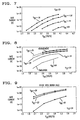
- the measured gate current I G of a MOSFET (a device as depicted in FIG. 2 without regions 160 and 170 wherein floating gate 140 functions as the gate electrode) with a 0.5 ⁇ m channel length and a 0.05 ⁇ m drain/source junction depth is depicted in FIG. 7 as a function of substrate bias (V BS ) and drain-source bias (V DS ) at a gate-source bias of 4V.
- the devices have gate oxides with a thickness of about 50 ⁇ .
- I G as a function of V BS is illustrated as a function of V DS for a MOSFET device with a channel length of 0.4 ⁇ m, a drain/source junction depth of about 0.07 ⁇ m, and a gate oxide thickness of about 60 ⁇ .
- V GS of 2V
- V BS when the V BS is decreased to about -1V to about -3V, then the requisite I G is obtained for V DS of about 2.2V to about 3V. As V BS increases, the amount of V DS needed to obtain the desired I G decreases.
- FIG. 9 is a graph of the relationship between V DS and I G for a MOSFET device with a boron halo which is the result of doping the substrate at the drain substrate junction.
- the device has a channel length of 0.4 ⁇ m and a drain/source junction depth of about 0.07 ⁇ m.
- the boron concentration is about 10 18 /cm 3 at the drain-substrate junction to achieve the desired effect.
- FIG. 9 illustrates that, at a V GS of 2V, the devices with a substrate bias provide acceptable gate current as described above at much lower V DS than does the device without a substrate bias. It follows that devices with the boron halo have acceptable gate current at lower V DS than devices without the boron halo when biased at the source voltages.
Landscapes
- Non-Volatile Memory (AREA)
- Semiconductor Memories (AREA)
- Read Only Memory (AREA)
- Solid State Image Pick-Up Elements (AREA)
Claims (20)
- Halbleiter-n-Kanal-Bauelement, das auf einem Substrat (100) ausgebildet ist, umfassend:gekennzeichnet durcheine Source-Zone (110) und eine Drain-Zone (120) in dem Substrat;ein dielektrische Schicht (150), die auf dem Substrat niedergeschlagen ist, eine schwimmende Gate-Elektrode (140), die auf der dielektrischen Schicht (150) gebildet ist, wobei zumindest ein Teil der schwimmenden Gate-Elektrode (140) über der Drain-Zone (120) liegt, auf der Oberfläche der schwimmenden Gate-Elektrode (140) ein zusätzliches dielektrisches Material (170) gebildet ist, und auf dem zusätzlichen dielektrischen Material (170) eine Steuergate-Elektrode (160) gebildet ist,
eine Einrichtung zum negativen Aufladen des schwimmenden Gates (140), mit einer Einrichtung (178) zum Anlegen einer negativen Substrat-Source-Vorspannung (VB - Vs) von etwa -0,5 Volt oder negativer, einer Einrichtung (177) zum Anlegen einer Steuergate-Source-Vorspannung (VC - VS) von etwa 10 Volt oder weniger, und einer Einrichtung (176) zum Anlegen einer Drain-Source-Vorspannung (VD - VS) von weniger als etwa 5 Volt an das Bauelement, wobei der das schwimmende Gate (140) aufladende Strom eingeleitet wird durch den von der Source zu dem Drain (120) fließenden Elektronenstrom. - Halbleiterbauelement nach Anspruch 1, bei dem die Vorspannung zwischen dem Substrat (100) und der Source (110) etwa -0,5 Volt bis etwa -3 Volt beim Aufladen des schwimmenden Gates (140) beträgt.
- Halbleiterbauelement nach Anspruch 1, bei dem die Vorspannung zwischen dem Steuer-Gate (160) und der Source (110) kleiner als die oder gleich der Drain-Source-Vorspannung ist.
- Halbleiterbauelement nach Anspruch 1, bei dem die Source-Spannung etwa 0 Volt beträgt, die Drain-Spannung etwa 1,1 bis 3,3 Volt beträgt und die Substratspannung etwa -0,5 bis etwa -3 Volt beim Laden des schwimmenden Gates (140) beträgt.
- Halbleiterbauelement nach Anspruch 1, bei dem die Steuergate-Spannung kleiner als die oder gleich der Drain-Spannung ist.
- Halbleiterbauelement nach Anspruch 1, bei dem das Substrat ein Zone aus Silicium-Germanium (402) aufweist.
- Halbleiterbauelement nach Anspruch 6, bei dem der Drain (120) in der Silicium-Germanium-Zone (402) gebildet ist und die Source (110) nicht in der Silicium-Germanium-Zone (402) gebildet ist.
- Halbleiterbauelement nach Anspruch 6, bei dem die Source (110) und der Drain (120) in der Silicium-Germanium-Zone (402) gebildet sind.
- Halbleiterbauelement nach Anspruch 1, bei dem das Bauelement ein n-Kanal-Bauelement mit gestapeltem Gate ist.
- Verfahren zum Laden eines schwimmenden n-Kanal-Gates einer Speicherzelle, die eine Source (110), einen Drain (120), ein Steuergate (160), ein schwimmendes Gate (140), von dem zumindest ein Teil über dem Drain liegt, und ein Substrat (100) aufweist, gekennzeichnet durch:Anlegen einer Spannung an den Drain-Anschluss (176) der Zelle, um eine positive Vorspannung von weniger als etwa 5 Volt zwischen dem Drain (120) und der Source (110) zu bewirken;Anlegen einer Spannung an den Steuergate-Anschluss (177) der Zelle, um eine positive Vorspannung von etwa 10 Volt oder weniger zwischen dem Steuergate (160) und der Source (110) zu bewirken; undAnlegen einer negativen Spannung an das Substrat (100), um eine negative Vorspannung von mindestens etwa -0,5 Volt zwischen dem Substrat (100) und der Source (110) zu bewirken, wobei der das schwimmende Gate (140) aufladende Strom eingeleitet wird durch den Elektronenstrom von der Source (110) zu dem Drain (120).
- Verfahren nach Anspruch 10, bei dem die negative Vorspannung zwischen dem Substrat (100) und der Source (110) etwa -0,5 Volt bis etwa -3 Volt beträgt.
- Verfahren nach Anspruch 10, bei dem die an die Source (110) angelegte Spannung Null beträgt, die an das Substrat (100) angelegte Spannung etwa -0,5 Volt bis etwa -3 Volt beträgt, die an das Steuergate (140) angelegte Spannung kleiner als etwa 10 Volt ist, und die an den Drain (120) angelegte Spannung etwa 1,1 Volt bis etwa 3,3 Volt beträgt.
- Verfahren nach Anspruch 12, bei dem die an das Steuergate (140) angelegte Spannung kleiner als die oder gleich der an den Drain (120) gelegten Spannung ist.
- Feld aus Speicherzellen (600) mit schwimmendem Gate, umfassend:mindestens zwei Halbleiter-n-Kanal-Bauelemente nach Anspruch 1, wobei das Substrat (100) von mindestens einem n-Kanal-Bauelement elektrisch an einen ersten Auswahlanschluss (611) angeschlossen ist, und das Substrat (100) von mindestens einem n-Kanal-Bauelement an einen zweiten Auswahlanschluss (612) angeschlossen ist, wobei der erste und der zweite Auswahlanschluss (611, 612) elektrisch voneinander isoliert sind.
- Feld nach Anspruch 14, bei dem die Vorspannung zwischen dem Drain (120) und der Source (110) jeder Zelle innerhalb des Feldes weniger als etwa 5 Volt beträgt, und die Substrat-Source-Vorspannung, die an das Substrat (100) in jeder Zelle innerhalb des Feldes gelegt wird, etwa -0,5 Volt bis etwa -3 Volt beim Aufladen des schwimmenden Gates (140) beträgt.
- Feld nach Anspruch 15, bei dem die an jede Zelle innerhalb des Feldes angelegte Source-Spannung etwa Null Volt beträgt, die Vorspannung zwischen dem Drain (120) und der Source (110) jeder Zelle innerhalb des Feldes etwa 1,1 Volt bis etwa 3,3 Volt beträgt, die an jede Zelle innerhalb des Feldes angelegte Drain-Spannung etwa 1,1 Volt bis etwa 3,3 Volt beträgt, und die Substratspannung etwa -0,5 Volt bis etwa -3 Volt beträgt, wenn das schwimmende Gate (140) aufgeladen wird.
- Feld nach Anspruch 16, bei dem die an das Steuergate (160) angelegte Spannung etwa 1,1 Volt bis etwa 3,3 Volt beträgt.
- Feld nach Anspruch 17, bei dem die an das Steuergate (160) angelegte Spannung kleiner als die oder gleich der an den Drain (120) angelegte Spannung ist.
- Bauelement nach Anspruch 1, bei der die an den Drain-Anschluss (176) angelegte Spannung eine positive Vorspannung von etwa 1,1 Volt bis etwa 3,3 Volt zwischen dem Drain (120) und der Source (110) hervorruft.
- Verfahren nach Anspruch 10, bei dem die an den Drain-Anschluss (176) der Zelle angelegte Spannung eine positive Vorspannung von etwa 1,1 Volt bis etwa 3,3 Volt hervorruft.
Applications Claiming Priority (2)
| Application Number | Priority Date | Filing Date | Title |
|---|---|---|---|
| US08/450,179 US5659504A (en) | 1995-05-25 | 1995-05-25 | Method and apparatus for hot carrier injection |
| US450179 | 1995-05-25 |
Publications (3)
| Publication Number | Publication Date |
|---|---|
| EP0744754A2 EP0744754A2 (de) | 1996-11-27 |
| EP0744754A3 EP0744754A3 (de) | 1999-03-17 |
| EP0744754B1 true EP0744754B1 (de) | 2004-12-01 |
Family
ID=23787097
Family Applications (1)
| Application Number | Title | Priority Date | Filing Date |
|---|---|---|---|
| EP96303419A Expired - Lifetime EP0744754B1 (de) | 1995-05-25 | 1996-05-15 | Verfahren und Vorrichtung für Injektion von heissen Ladungsträgern |
Country Status (5)
| Country | Link |
|---|---|
| US (2) | US5659504A (de) |
| EP (1) | EP0744754B1 (de) |
| JP (1) | JPH08330456A (de) |
| KR (1) | KR100392855B1 (de) |
| DE (1) | DE69633958T2 (de) |
Families Citing this family (43)
| Publication number | Priority date | Publication date | Assignee | Title |
|---|---|---|---|---|
| US5978272A (en) * | 1995-06-07 | 1999-11-02 | Advanced Micro Devices, Inc. | Nonvolatile memory structure for programmable logic devices |
| US5834355A (en) * | 1996-12-31 | 1998-11-10 | Intel Corporation | Method for implanting halo structures using removable spacer |
| EP0908895A1 (de) | 1997-10-09 | 1999-04-14 | STMicroelectronics S.r.l. | Reguliertes Heiss-Elektronen-Schreibverfahren für nicht-flüchtige Speicherzellen |
| US6009017A (en) | 1998-03-13 | 1999-12-28 | Macronix International Co., Ltd. | Floating gate memory with substrate band-to-band tunneling induced hot electron injection |
| US6002610A (en) * | 1998-04-30 | 1999-12-14 | Lucent Technologies Inc. | Non-volatile memory element for programmable logic applications and operational methods therefor |
| US6185133B1 (en) | 1998-06-26 | 2001-02-06 | Amic Technology, Inc. | Flash EPROM using junction hot hole injection for erase |
| KR100276653B1 (ko) | 1998-08-27 | 2001-01-15 | 윤종용 | 스프릿 게이트형 불휘발성 메모리 셀의 구동방법 및 이 셀들을구비한 반도체 메모리 장치의 구동방법 |
| US6011722A (en) * | 1998-10-13 | 2000-01-04 | Lucent Technologies Inc. | Method for erasing and programming memory devices |
| EP1096572B8 (de) * | 1999-10-25 | 2009-09-02 | Imec | Elektrisch programmierbares und löschbares Gerät und ein Verfahren zu seinem Betrieb |
| US6518122B1 (en) | 1999-12-17 | 2003-02-11 | Chartered Semiconductor Manufacturing Ltd. | Low voltage programmable and erasable flash EEPROM |
| US6850440B2 (en) | 1999-12-27 | 2005-02-01 | Winbond Electronics Corporation | Method for improved programming efficiency in flash memory cells |
| US6363012B1 (en) | 1999-12-27 | 2002-03-26 | Winbond Electronics Corporation | Method for improved programming efficiency in flash memory cells |
| TW473724B (en) * | 2000-05-17 | 2002-01-21 | Winbond Electronics Corp | Method using source bias for executing a write operation to the nonvolatile memory cell |
| US6313486B1 (en) | 2000-06-15 | 2001-11-06 | Board Of Regents, The University Of Texas System | Floating gate transistor having buried strained silicon germanium channel layer |
| US6313487B1 (en) | 2000-06-15 | 2001-11-06 | Board Of Regents, The University Of Texas System | Vertical channel floating gate transistor having silicon germanium channel layer |
| US6528845B1 (en) | 2000-07-14 | 2003-03-04 | Lucent Technologies Inc. | Non-volatile semiconductor memory cell utilizing trapped charge generated by channel-initiated secondary electron injection |
| EP1178540B1 (de) * | 2000-07-31 | 2014-10-22 | Micron Technology, Inc. | Nichtflüchtige Speicherzelle mit hoher Programmierungsleistung |
| US6747899B2 (en) * | 2001-05-14 | 2004-06-08 | Nexflash Technologies, Inc. | Method and apparatus for multiple byte or page mode programming of a flash memory array |
| US6731544B2 (en) * | 2001-05-14 | 2004-05-04 | Nexflash Technologies, Inc. | Method and apparatus for multiple byte or page mode programming of a flash memory array |
| US6459615B1 (en) | 2001-07-23 | 2002-10-01 | Agere Systems Guardian Corp. | Non-volatile memory cell array with shared erase device |
| US6590810B2 (en) * | 2001-08-15 | 2003-07-08 | Winbond Electronics Corporation | Source biasing circuit for flash EEPROM |
| US6512700B1 (en) | 2001-09-20 | 2003-01-28 | Agere Systems Inc. | Non-volatile memory cell having channel initiated secondary electron injection programming mechanism |
| US6870213B2 (en) * | 2002-05-10 | 2005-03-22 | International Business Machines Corporation | EEPROM device with substrate hot-electron injector for low-power |
| US6826080B2 (en) * | 2002-05-24 | 2004-11-30 | Nexflash Technologies, Inc. | Virtual ground nonvolatile semiconductor memory array architecture and integrated circuit structure therefor |
| US6791883B2 (en) | 2002-06-24 | 2004-09-14 | Freescale Semiconductor, Inc. | Program and erase in a thin film storage non-volatile memory |
| JP4049641B2 (ja) * | 2002-09-06 | 2008-02-20 | 株式会社ルネサステクノロジ | 不揮発性半導体記憶装置 |
| TWI244165B (en) * | 2002-10-07 | 2005-11-21 | Infineon Technologies Ag | Single bit nonvolatile memory cell and methods for programming and erasing thereof |
| US6819593B2 (en) * | 2002-12-13 | 2004-11-16 | Taiwan Semiconductor Manufacturing Company | Architecture to suppress bit-line leakage |
| WO2004058078A1 (en) * | 2002-12-16 | 2004-07-15 | Edrich Vascular Devices, Inc. | Multiple stapling device for narrow blood vessels |
| US6713810B1 (en) * | 2003-02-10 | 2004-03-30 | Micron Technology, Inc. | Non-volatile devices, and electronic systems comprising non-volatile devices |
| US6768671B1 (en) | 2003-03-05 | 2004-07-27 | Nexflash Technologies, Inc. | Nonvolatile memory and method of operation thereof to control erase disturb |
| CN100463138C (zh) * | 2004-04-26 | 2009-02-18 | 旺宏电子股份有限公司 | 电荷陷入非易失性存储器的电荷平衡操作方法 |
| TWI231039B (en) * | 2004-04-30 | 2005-04-11 | Yield Microelectronics Corp | Non-volatile memory and its operational method |
| US7195983B2 (en) * | 2004-08-31 | 2007-03-27 | Freescale Semiconductor, Inc. | Programming, erasing, and reading structure for an NVM cell |
| US7105395B2 (en) * | 2004-08-31 | 2006-09-12 | Freescale Semiconductor, Inc. | Programming and erasing structure for an NVM cell |
| US7200045B2 (en) * | 2004-12-30 | 2007-04-03 | Macronix International Company, Ltd. | Method for programming a charge-trapping nonvolatile memory cell by raised-Vs channel initialed secondary electron injection (CHISEL) |
| JP4690948B2 (ja) | 2006-03-31 | 2011-06-01 | 東芝ストレージデバイス株式会社 | 位置決め制御装置の整定判定方法及び位置決め制御装置 |
| US7626864B2 (en) * | 2006-04-26 | 2009-12-01 | Chih-Hsin Wang | Electrically alterable non-volatile memory cells and arrays |
| JP4991201B2 (ja) | 2006-07-28 | 2012-08-01 | 株式会社東芝 | 位置決め制御装置の整定判定方法及び位置決め制御装置 |
| US7687856B2 (en) * | 2007-05-10 | 2010-03-30 | Texas Instruments Incorporated | Body bias to facilitate transistor matching |
| US7916551B2 (en) * | 2007-11-06 | 2011-03-29 | Macronix International Co., Ltd. | Method of programming cell in memory and memory apparatus utilizing the method |
| US8139418B2 (en) * | 2009-04-27 | 2012-03-20 | Micron Technology, Inc. | Techniques for controlling a direct injection semiconductor memory device |
| US9343468B1 (en) * | 2015-03-26 | 2016-05-17 | Texas Instruments Incorporated | Feed-forward bidirectional implanted split-gate flash memory cell |
Family Cites Families (21)
| Publication number | Priority date | Publication date | Assignee | Title |
|---|---|---|---|---|
| US5168208A (en) * | 1988-05-09 | 1992-12-01 | Onan Corporation | Microprocessor based integrated generator set controller apparatus and method |
| US5042009A (en) * | 1988-12-09 | 1991-08-20 | Waferscale Integration, Inc. | Method for programming a floating gate memory device |
| KR940010930B1 (ko) * | 1990-03-13 | 1994-11-19 | 가부시키가이샤 도시바 | 반도체장치의 제조방법 |
| US5222040A (en) * | 1990-12-11 | 1993-06-22 | Nexcom Technology, Inc. | Single transistor eeprom memory cell |
| US5295095A (en) * | 1991-08-22 | 1994-03-15 | Lattice Semiconductor Corporation | Method of programming electrically erasable programmable read-only memory using particular substrate bias |
| US5278439A (en) * | 1991-08-29 | 1994-01-11 | Ma Yueh Y | Self-aligned dual-bit split gate (DSG) flash EEPROM cell |
| US5364806A (en) * | 1991-08-29 | 1994-11-15 | Hyundai Electronics Industries Co., Ltd. | Method of making a self-aligned dual-bit split gate (DSG) flash EEPROM cell |
| US5327378A (en) * | 1992-03-04 | 1994-07-05 | Waferscale Integration, Inc. | Easily manufacturable compact EPROM |
| JP3765585B2 (ja) * | 1992-08-10 | 2006-04-12 | 株式会社ルネサステクノロジ | データ処理装置 |
| JP2771729B2 (ja) * | 1992-04-16 | 1998-07-02 | 三菱電機株式会社 | チャージポンプ回路 |
| US5357463A (en) * | 1992-11-17 | 1994-10-18 | Micron Semiconductor, Inc. | Method for reverse programming of a flash EEPROM |
| US5381051A (en) * | 1993-03-08 | 1995-01-10 | Motorola Inc. | High voltage charge pump |
| US5471423A (en) * | 1993-05-17 | 1995-11-28 | Nippon Steel Corporation | Non-volatile semiconductor memory device |
| JP2974547B2 (ja) * | 1993-05-17 | 1999-11-10 | 新日本製鐵株式会社 | 半導体記憶装置の製造方法 |
| US5357476A (en) * | 1993-06-01 | 1994-10-18 | Motorola, Inc. | Apparatus and method for erasing a flash EEPROM |
| US5349220A (en) * | 1993-08-10 | 1994-09-20 | United Microelectronics Corporation | Flash memory cell and its operation |
| US5412603A (en) * | 1994-05-06 | 1995-05-02 | Texas Instruments Incorporated | Method and circuitry for programming floating-gate memory cell using a single low-voltage supply |
| US5487033A (en) * | 1994-06-28 | 1996-01-23 | Intel Corporation | Structure and method for low current programming of flash EEPROMS |
| US5511021A (en) * | 1995-02-22 | 1996-04-23 | National Semiconductor Corporation | Method for programming a single EPROM or flash memory cell to store multiple levels of data that utilizes a forward-biased source-to-substrate junction |
| US5491657A (en) * | 1995-02-24 | 1996-02-13 | Advanced Micro Devices, Inc. | Method for bulk (or byte) charging and discharging an array of flash EEPROM memory cells |
| US5546340A (en) * | 1995-06-13 | 1996-08-13 | Advanced Micro Devices, Inc. | Non-volatile memory array with over-erase correction |
-
1995
- 1995-05-25 US US08/450,179 patent/US5659504A/en not_active Expired - Lifetime
-
1996
- 1996-05-15 EP EP96303419A patent/EP0744754B1/de not_active Expired - Lifetime
- 1996-05-15 DE DE69633958T patent/DE69633958T2/de not_active Expired - Lifetime
- 1996-05-25 KR KR1019960017845A patent/KR100392855B1/ko not_active Expired - Lifetime
- 1996-05-27 JP JP13169696A patent/JPH08330456A/ja active Pending
-
1997
- 1997-07-03 US US08/888,030 patent/US5838617A/en not_active Expired - Lifetime
Also Published As
| Publication number | Publication date |
|---|---|
| KR100392855B1 (ko) | 2003-10-11 |
| KR960043250A (ko) | 1996-12-23 |
| EP0744754A3 (de) | 1999-03-17 |
| DE69633958D1 (de) | 2005-01-05 |
| EP0744754A2 (de) | 1996-11-27 |
| US5659504A (en) | 1997-08-19 |
| JPH08330456A (ja) | 1996-12-13 |
| US5838617A (en) | 1998-11-17 |
| DE69633958T2 (de) | 2005-12-22 |
Similar Documents
| Publication | Publication Date | Title |
|---|---|---|
| US5659504A (en) | Method and apparatus for hot carrier injection | |
| US6172397B1 (en) | Non-volatile semiconductor memory device | |
| KR0184024B1 (ko) | 불휘발성 반도체기억장치 및 그 동작방법 | |
| US5687118A (en) | PMOS memory cell with hot electron injection programming and tunnelling erasing | |
| US6088269A (en) | Compact page-erasable EEPROM non-volatile memory | |
| EP0974146B1 (de) | Nichtflüchtiger speicher | |
| US6563741B2 (en) | Flash memory device and method of erasing | |
| KR100485985B1 (ko) | 스케일러블 플래시 eeprom 메모리 셀의 제작 및 작동 방법 | |
| US6828618B2 (en) | Split-gate thin-film storage NVM cell | |
| US5329487A (en) | Two transistor flash EPROM cell | |
| US6352886B2 (en) | Method of manufacturing floating gate memory with substrate band-to-band tunneling induced hot electron injection | |
| US5790460A (en) | Method of erasing a flash EEPROM memory | |
| EP1687826A2 (de) | Flash-speicher-programmierung durch verwendung von gate-induziertem sperrschichtleckstrom | |
| US5521867A (en) | Adjustable threshold voltage conversion circuit | |
| EP0994487A1 (de) | Verfahren zum Löschen und Programmieren von Speicheranordnungen | |
| US6243298B1 (en) | Non-volatile memory cell capable of being programmed and erased through substantially separate areas of one of its drain-side and source-side regions | |
| KR100861749B1 (ko) | 2t nor형 비휘발성 메모리 셀 어레이, 2t nor형비휘발성 메모리의 데이터 처리방법 | |
| US6473342B2 (en) | Methods of operating split-gate type non-volatile memory cells | |
| US7372734B2 (en) | Methods of operating electrically alterable non-volatile memory cell | |
| US6653682B1 (en) | Non-volatile electrically alterable semiconductor memory device | |
| US6528845B1 (en) | Non-volatile semiconductor memory cell utilizing trapped charge generated by channel-initiated secondary electron injection | |
| US6850440B2 (en) | Method for improved programming efficiency in flash memory cells | |
| US6768683B1 (en) | Low column leakage flash memory array | |
| EP0463331A2 (de) | Verbessertes Verfahren zur Programmierung eines nichtflüchtigen Speichers |
Legal Events
| Date | Code | Title | Description |
|---|---|---|---|
| PUAI | Public reference made under article 153(3) epc to a published international application that has entered the european phase |
Free format text: ORIGINAL CODE: 0009012 |
|
| AK | Designated contracting states |
Kind code of ref document: A2 Designated state(s): DE FR GB |
|
| PUAL | Search report despatched |
Free format text: ORIGINAL CODE: 0009013 |
|
| AK | Designated contracting states |
Kind code of ref document: A3 Designated state(s): DE FR GB |
|
| 17P | Request for examination filed |
Effective date: 19990902 |
|
| 17Q | First examination report despatched |
Effective date: 20010620 |
|
| GRAP | Despatch of communication of intention to grant a patent |
Free format text: ORIGINAL CODE: EPIDOSNIGR1 |
|
| GRAS | Grant fee paid |
Free format text: ORIGINAL CODE: EPIDOSNIGR3 |
|
| GRAA | (expected) grant |
Free format text: ORIGINAL CODE: 0009210 |
|
| AK | Designated contracting states |
Kind code of ref document: B1 Designated state(s): DE FR GB |
|
| REG | Reference to a national code |
Ref country code: GB Ref legal event code: FG4D |
|
| REF | Corresponds to: |
Ref document number: 69633958 Country of ref document: DE Date of ref document: 20050105 Kind code of ref document: P |
|
| PLBE | No opposition filed within time limit |
Free format text: ORIGINAL CODE: 0009261 |
|
| STAA | Information on the status of an ep patent application or granted ep patent |
Free format text: STATUS: NO OPPOSITION FILED WITHIN TIME LIMIT |
|
| ET | Fr: translation filed | ||
| 26N | No opposition filed |
Effective date: 20050902 |
|
| PGFP | Annual fee paid to national office [announced via postgrant information from national office to epo] |
Ref country code: FR Payment date: 20140509 Year of fee payment: 19 |
|
| REG | Reference to a national code |
Ref country code: DE Ref legal event code: R082 Ref document number: 69633958 Country of ref document: DE Representative=s name: DILG HAEUSLER SCHINDELMANN PATENTANWALTSGESELL, DE |
|
| PGFP | Annual fee paid to national office [announced via postgrant information from national office to epo] |
Ref country code: DE Payment date: 20150422 Year of fee payment: 20 Ref country code: GB Payment date: 20150424 Year of fee payment: 20 |
|
| REG | Reference to a national code |
Ref country code: FR Ref legal event code: ST Effective date: 20160129 |
|
| REG | Reference to a national code |
Ref country code: DE Ref legal event code: R071 Ref document number: 69633958 Country of ref document: DE |
|
| PG25 | Lapsed in a contracting state [announced via postgrant information from national office to epo] |
Ref country code: FR Free format text: LAPSE BECAUSE OF NON-PAYMENT OF DUE FEES Effective date: 20150601 |
|
| REG | Reference to a national code |
Ref country code: GB Ref legal event code: PE20 Expiry date: 20160514 |
|
| PG25 | Lapsed in a contracting state [announced via postgrant information from national office to epo] |
Ref country code: GB Free format text: LAPSE BECAUSE OF EXPIRATION OF PROTECTION Effective date: 20160514 |