EP0743625A2 - Signalversorgter frequenzteilender Transponder - Google Patents
Signalversorgter frequenzteilender Transponder Download PDFInfo
- Publication number
- EP0743625A2 EP0743625A2 EP96650009A EP96650009A EP0743625A2 EP 0743625 A2 EP0743625 A2 EP 0743625A2 EP 96650009 A EP96650009 A EP 96650009A EP 96650009 A EP96650009 A EP 96650009A EP 0743625 A2 EP0743625 A2 EP 0743625A2
- Authority
- EP
- European Patent Office
- Prior art keywords
- resonant circuit
- frequency
- capacitance
- electromagnetic radiation
- series
- Prior art date
- Legal status (The legal status is an assumption and is not a legal conclusion. Google has not performed a legal analysis and makes no representation as to the accuracy of the status listed.)
- Granted
Links
Images

Classifications
-
- G—PHYSICS
- G08—SIGNALLING
- G08B—SIGNALLING SYSTEMS, e.g. PERSONAL CALLING SYSTEMS; ORDER TELEGRAPHS; ALARM SYSTEMS
- G08B13/00—Burglar, theft or intruder alarms
- G08B13/22—Electrical actuation
- G08B13/24—Electrical actuation by interference with electromagnetic field distribution
- G08B13/2402—Electronic Article Surveillance [EAS], i.e. systems using tags for detecting removal of a tagged item from a secure area, e.g. tags for detecting shoplifting
- G08B13/2405—Electronic Article Surveillance [EAS], i.e. systems using tags for detecting removal of a tagged item from a secure area, e.g. tags for detecting shoplifting characterised by the tag technology used
- G08B13/2422—Electronic Article Surveillance [EAS], i.e. systems using tags for detecting removal of a tagged item from a secure area, e.g. tags for detecting shoplifting characterised by the tag technology used using acoustic or microwave tags
-
- G—PHYSICS
- G08—SIGNALLING
- G08B—SIGNALLING SYSTEMS, e.g. PERSONAL CALLING SYSTEMS; ORDER TELEGRAPHS; ALARM SYSTEMS
- G08B13/00—Burglar, theft or intruder alarms
- G08B13/22—Electrical actuation
- G08B13/24—Electrical actuation by interference with electromagnetic field distribution
- G08B13/2402—Electronic Article Surveillance [EAS], i.e. systems using tags for detecting removal of a tagged item from a secure area, e.g. tags for detecting shoplifting
- G08B13/2428—Tag details
- G08B13/2431—Tag circuit details
-
- G—PHYSICS
- G08—SIGNALLING
- G08B—SIGNALLING SYSTEMS, e.g. PERSONAL CALLING SYSTEMS; ORDER TELEGRAPHS; ALARM SYSTEMS
- G08B13/00—Burglar, theft or intruder alarms
- G08B13/22—Electrical actuation
- G08B13/24—Electrical actuation by interference with electromagnetic field distribution
- G08B13/2402—Electronic Article Surveillance [EAS], i.e. systems using tags for detecting removal of a tagged item from a secure area, e.g. tags for detecting shoplifting
- G08B13/2428—Tag details
- G08B13/2434—Tag housing and attachment details
-
- G—PHYSICS
- G08—SIGNALLING
- G08B—SIGNALLING SYSTEMS, e.g. PERSONAL CALLING SYSTEMS; ORDER TELEGRAPHS; ALARM SYSTEMS
- G08B13/00—Burglar, theft or intruder alarms
- G08B13/22—Electrical actuation
- G08B13/24—Electrical actuation by interference with electromagnetic field distribution
- G08B13/2402—Electronic Article Surveillance [EAS], i.e. systems using tags for detecting removal of a tagged item from a secure area, e.g. tags for detecting shoplifting
- G08B13/2451—Specific applications combined with EAS
- G08B13/2462—Asset location systems combined with EAS
Definitions
- the present invention generally pertains to batteryless, portable frequency dividers such as are used as miniature signal-powered transponders in presence detection systems. Presence detection systems are useful for article surveillance and article-location determination. Batteryless, portable frequency dividers are described in U.S. Patent No. 5,241,298 to Ming R. Lian and Fred W. Herman, U. S. Patent No. 4,481,428 to Lincoln H. Charlot, Jr., U.S. Patent No. 4,670,740 to Fred W. Herman and Lincoln H. Charlot, Jr. and U.S. Patent No. 4,314,373 to Robert W. Sellers.
- the frequency dividers described in U.S. Patents Nos. 5,241,298; 4,481,428 and 4,314,373 each comprises a first parallel resonant circuit including an inductance and a capacitance that is resonant at a first frequency for receiving electromagnetic radiation at a first frequency and a second parallel resonant circuit including an inductance and a capacitance that is resonant at a second frequency that is one-half the first frequency for transmitting electromagnetic radiation at the second frequency.
- the capacitance of one or both of the resonant circuits is a variable capacitance element in which the capacitance varies in accordance with the voltage across the variable capacitance element; and variation of the capacitance of the variable capacitance element in response to variations in energy in the first resonant circuit resulting from the first resonant circuit receiving electromagnetic radiation at the first frequency causes the second resonant circuit to transmit electromagnetic radiation at the second frequency.
- the two resonant circuits are magnetically coupled to one another or electrically connected through an electrical coupling element, such as an additional coupling capacitor or a semiconductor element.
- the two resonant circuits are electrically connected to one another by a semiconductor switching device that couples the first resonant circuit to the second resonant circuit to cause the second resonant circuit to transmit electromagnetic radiation at the second frequency in response to receipt of radiation at the first frequency.
- the resonant circuit inductances contain both in-phase and out-of-phase currents and the inductance coils are disposed perpendicular to each other so that the magnetic fields of the two coils are orthogonal in order to avoid cancellation of fields and a resulting decrease in efficiency.
- the resonant circuits are coupled to one another through a variable capacitance element, such as a varactor diode, to cause the second resonant circuit to transmit electromagnetic radiation at the second frequency in response to receipt of electromagnetic radiation by the first resonant circuit at the first frequency
- the frequency divider described in U.S. Patent No. 4,670,740 consists of a parallel resonant circuit including an inductance and variable capacitance device that is resonant at a second frequency that is one-half a first frequency to cause the circuit to transmit electromagnetic radiation at the second frequency in response to receipt of electromagnetic radiation at the first frequency.
- the present invention provides a batteryless, portable frequency divider, comprising a first resonant circuit including an inductance and a capacitance that is resonant at a first frequency for receiving electromagnetic radiation at a first frequency; and a second resonant circuit including an inductance and a capacitance that is resonant at a second frequency that is 1/n the first frequency for transmitting electromagnetic energy at the second frequency, wherein "n" is an integer greater than one; wherein one of the resonant circuits is a series resonant circuit and the other of the resonant circuits is a parallel resonant circuit; wherein the first resonant circuit is connected directly across the second resonant circuit; and wherein the frequency divider includes an element for causing the second resonant circuit to transmit electromagnetic radiation at the second frequency in response to variations in energy in the first resonant circuit resulting from the first resonant circuit receiving electromagnetic radiation at the first frequency.
- the frequency divider of the present invention is highly efficient so as to be detectable over a large range and is stable in sensitivity (or detection range) due to the direct connection of the two resonant circuits.
- the direct connection of the resonant circuits also reduces the effect of magnetic coupling of the circuits and allows use of a common ferrite core for the inductance coils of the two circuits.
- one of the two resonant circuits must be a series resonant circuit in order to define two discrete resonant circuits.
- the capacitance of one or both of the resonant circuits is a variable capacitance element in which the capacitance varies in accordance with the voltage across the variable capacitance element; and variation of the capacitance of the variable capacitance element in response to variations in energy in the first resonant circuit resulting from the first resonant circuit receiving electromagnetic radiation at the first frequency causes the second resonant circuit to transmit electromagnetic radiation at the second frequency.
- the frequency divider includes a three-terminal semiconductor switching device having a control terminal, a reference terminal, and a controlled terminal; the first resonant circuit is a parallel resonant circuit and the second resonant circuit is a series resonant circuit; and the semiconductor switching device is connected directly across both resonant circuits and between the inductance and the capacitance of the series resonant circuit and switches on and off in response to variations in energy in the parallel resonant circuit resulting from the parallel resonant circuit receiving electromagnetic radiation at the first frequency to cause the series resonant circuit to transmit electromagnetic radiation at the second frequency.
- the present invention further provides a tag for attachment to an article to be detected within a surveillance zone of an electronic article surveillance system, wherein the tag includes the frequency divider of the present invention as a transponder for detecting electromagnetic radiation of a first predetermined frequency and responding to said detection by transmitting electromagnetic radiation of a second predetermined frequency that is a plural-integer-divided quotient of the first predetermined frequency; a container for housing the transponder and means for use in attaching the container to the article to be detected.
- the present invention also provides a tag for attachment to a buried article to enable the buried article to be located by detecting the presence of the tag, wherein the tag includes the frequency divider of the present invention as a transponder for detecting electromagnetic radiation of a first predetermined frequency and responding to said detection by transmitting electromagnetic radiation of a second predetermined frequency that is a plural-integer-divided quotient of the first predetermined frequency; and a sealed container housing the transponder to protect the transponder from moisture.
- FIG. 1 is a schematic circuit diagram of one preferred embodiment of a frequency divider according to the present invention.
- FIG. 2 is a graph showing the field intensity of electromagnetic radiation transmitted by the second resonant (output) circuit in relation to the field intensity of electromagnetic radiation received by the first resonant (input) circuit in the frequency divider of FIG. 1 .
- FIG. 3 is a schematic circuit diagram of another preferred embodiment of a frequency divider according to the present invention.
- FIG. 4 is a schematic circuit diagram of a further preferred embodiment of a frequency divider according to the present invention.
- FIG. 5 shows waveforms of the voltages at the terminals of the frequency divider of FIG. 4 to which the base and the collector of the transistor Q1 are respectively connected with respect to the voltage at the terminal to which the emitter of the transistor Q1 is connected.
- FIG. 6 is a schematic circuit diagram of still another preferred embodiment of a frequency divider according to the present invention.
- FIG. 7 is plan view of a tag containing a frequency-dividing transponder for use in an electronic article surveillance system, wherein portions of the tag are broken away to show the casing of a clutch mechanism and the inductance components of the frequency dividing transponder.
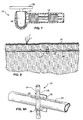
- FIG. 8 is a sectional view illustrating a tag containing a frequency-dividing transponder attached to a buried conduit.
- FIG. 8A is an enlarged view of the tag shown in Figure 8 , with the transponder contained therein being shown with dashed lines.
- the frequency divider includes a series resonant circuit including an inductance L1 and a capacitance C1 and a parallel resonant circuit including an inductance L2 and a varactor D2 .
- the varactor D2 is a variable capacitance element in which the capacitance varies in accordance with the voltage across the variable capacitance element
- the series resonant circuit L1-C1 is connected directly across the parallel resonant circuit L2-D2 at the terminals X and Y .
- the values of the respective components of the series resonant circuit L1-C1 and the parallel resonant circuit L2-D2 are selected so that the series resonant circuit L1-C1 is resonant at a first frequency for receiving electromagnetic radiation at a first frequency and the parallel resonant circuit L2-D2 is resonant at a second frequency that is one-half the first frequency for transmitting electromagnetic energy at the second frequency.
- the variation of the capacitance of the varactor D2 in response to variations in energy in the series resonant circuit L1-C1 resulting from the series resonant circuit L1-C1 receiving electromagnetic radiation at the first frequency causes the parallel resonant circuit L2-D2 to transmit electromagnetic radiation at the second frequency.
- the component values required for resonance of the series resonant circuit L1-C1 and the parallel resonant circuit L2-D2 may not be chosen independently from each other due to the direct interconnection of the series and parallel resonant circuits, but must be chosen as a set of values simultaneously selected for all four components.
- FIG. 2 shows the field intensity of electromagnetic radiation transmitted by the parallel resonant (output) circuit L2-D2 , in nano-Teslas, in relation to the field intensity of electromagnetic radiation received by the series resonant (input) circuit L1-C1 , also in nano-Teslas, in the frequency divider of FIG. 1 .
- the values of the respective components of the series resonant circuit L1-C1 and the parallel resonant circuit L2-D2 are selected so that the parallel resonant circuit L2-D2 is resonant at a first frequency for receiving electromagnetic radiation at a first frequency and the series resonant circuit L1-C1 is resonant at a second frequency that is one-half the first frequency for transmitting electromagnetic energy at the second frequency.
- the variation of the capacitance of the varactor D2 in response to variations in energy in the parallel resonant circuit L2-D2 resulting from the parallel resonant circuit L2-D2 receiving electromagnetic radiation at the first frequency causes the series resonant circuit L1-C1 to transmit electromagnetic radiation at the second frequency.
- the frequency divider includes a series resonant circuit including an inductance L1 and a varactor D1 and a parallel resonant circuit including an inductance L2 and a capacitance C2 .
- the varactor D1 is a variable capacitance element in which the capacitance varies in accordance with the voltage across the variable capacitance element
- the series resonant circuit L1-D1 is connected directly across the parallel resonant circuit L2-C2 at the terminals X and Y .
- the values of the respective components of the series resonant circuit L1-D1 and the parallel resonant circuit L2-C2 are selected so that the series resonant circuit L1-D1 is resonant at a first frequency for receiving electromagnetic radiation at a first frequency and the parallel resonant circuit L2-C2 is resonant at a second frequency that is one-half the first frequency for transmitting electromagnetic energy at the second frequency.
- the variation of the capacitance of the varactor D1 in response to variations in energy in the series resonant circuit L1-D1 resulting from the series resonant circuit L1-D1 receiving electromagnetic radiation at the first frequency causes the parallel resonant circuit L2-C2 to transmit electromagnetic radiation at the second frequency.
- the component values required for resonance of the series resonant circuit L1-D1 and the parallel resonant circuit L2-C2 may not be chosen independently from each other due to the direct interconnection of the series and parallel resonant circuits, but must be chosen as a set of values simultaneously selected for all four components.
- the resonant frequency of the series resonant circuit L1-D1 is 132 kHz.
- the resonant frequency of the parallel resonant circuit L2-C2 is 66 kHz.
- the values of the respective components of the series resonant circuit L1-C1 and the parallel resonant circuit L2-D2 are selected so that the parallel resonant circuit L2-C2 is resonant at a first frequency for receiving electromagnetic radiation at a first frequency and the series resonant circuit L1-D1 is resonant at a second frequency that is one-half the first frequency for transmitting electromagnetic energy at the second frequency.
- the variation of the capacitance of the varactor D1 in response to variations in energy in the parallel resonant circuit L2-C2 resulting from the parallel resonant circuit L2-C2 receiving electromagnetic radiation at the first frequency causes the series resonant circuit L1-D1 to transmit electromagnetic radiation at the second frequency.
- the frequency divider of FIG. 3 is modified by substituting a varactor having a zero-voltage capacitance of 3,300 pf. for the capacitance C2 in the parallel resonant circuit.
- the operation of this embodiment is as described above with reference to FIGS. 1 and 3 .
- the frequency divider includes a series resonant circuit including an inductance L1 and a capacitance C1 , a parallel resonant circuit including an inductance L2 and a capacitance C2 , and a semiconductor switching device, to wit: an npn bipolar transistor Q1 .
- the values of the respective components of the series resonant circuit L1-C1 and the parallel resonant circuit L2-C2 are selected so that the parallel resonant circuit L2-C2 is resonant at a first frequency for receiving electromagnetic radiation at a first frequency and the series resonant circuit L1-C1 is resonant at a second frequency that is one-half the first frequency for transmitting electromagnetic energy at the second frequency.
- the series resonant circuit L1-C1 is connected directly across the parallel resonant circuit L2-C2 at the terminals X and Y .
- the transistor Q1 is connected to series resonant circuit L1-C1 as a three-terminal semiconductor switching device so that its base functions as a control terminal, its emitter functions as a reference terminal, and its collector functions as a controlled terminal.
- the transistor Q1 is connected directly across both resonant circuits L1-C1 and L2-C2 and between the inductance L1 and the capacitance C1 of the series resonant circuit with its control terminal (base) connected to a terminal X that is common to the parallel resonant circuit and the capacitance C1 of the series resonant circuit, with its reference terminal (emitter) connected to a terminal Y that is common to the parallel resonant circuit and the inductance L1 of the series resonant circuit and with its controlled terminal (collector) connected to a terminal Z which is connected between the capacitance C1 and the inductance L1 of the series resonant circuit so that the transistor Q1 switches on and off in response to variations in energy in the parallel resonant circuit L2-C2 resulting from the parallel resonant circuit L2-C2 receiving electromagnetic radiation at the first frequency to cause the series resonant circuit L1-C1 to transmit electromagnetic radiation at the second frequency.
- FIG. 5 The waveforms of the voltages at the terminals X and Z of the frequency divider of FIG. 4 to which the base and the collector of the transistor Q1 are respectively connected with respect to the voltage at the emitter-connected terminal Z are shown in FIG. 5.
- the forward-biased voltage FB is shown above the abscissa and the reverse-biased voltage RB is shown below the abscissa.
- the shaded portions of these waveforms show the forward-biased portion of the voltage between the control terminal X and the reference terminal Y ; and both the forward-biased and the reverse-biased portions of the voltage between the controlled terminal Z and the reference terminal Y .
- the inductance L1 of the series resonant circuit is shunted during alternate forward-biased half-cycles of the energy at the first frequency f1 across the parallel resonant circuit L2-C2 between the terminals X and Y . These are the first and third cycles of the X-Y waveform illustrated in FIG. 5 .
- the controlled terminal (collector) is reverse biased with respect to the reference terminal (emitter) during alternate cycles so that no shunting then occurs, which includes the second cycle of the X-Y waveform, thereby enabling frequency division in the series resonant circuit L1-C1 .
- Frequency division occurs by the switching action of transistor Q1 shunting the collector-to-emitter voltage across the inductance L1 during each forward-biased portion of the voltage between the terminals Z and Y .
- This action causes a small field energy to be induced in the inductance L1 to start the inductance L1 ringing at its characteristic resonant frequency.
- no shunting action occurs so that ringing of the series resonant circuit L1-C1 is sustained at the characteristic resonant frequency f2 of the series resonant circuit L1-C1 .
- the component values required for resonance of the series resonant circuit L1-C1 and the parallel resonant circuit L2-C2 may not be chosen independently from each other due to the direct interconnection of the series and parallel resonant circuits, but must be chosen as a set of values simultaneously selected for all four components.
- the frequency divider includes a series resonant circuit including an inductance L1 and a capacitance C1 , a parallel resonant circuit including an inductance L2 and a capacitance C2 , and a semiconductor switching device, to wit: an npn bipolar transistor Q2 .
- the values of the respective components of the series resonant circuit L1-C1 and the parallel resonant circuit L2-C2 are selected so that the parallel resonant circuit L2-C2 is resonant at a first frequency for receiving electromagnetic radiation at a first frequency and the series resonant circuit L1-C1 is resonant at a second frequency that is one-half the first frequency for transmitting electromagnetic energy at the second frequency.
- the series resonant circuit L1-C1 is connected directly across the parallel resonant circuit L2-C2 at the terminals X and Y .
- the transistor Q2 is connected to series resonant circuit L1-C1 as a three-terminal semiconductor switching device so that its base functions as a control terminal, its emitter functions as a reference terminal, and its collector functions as a controlled terminal.
- the transistor Q2 is connected directly across both resonant circuits L1-C1 and L2-C2 and between the inductance L1 and the capacitance C1 of the series resonant circuit with its controlled terminal (collector) connected to a terminal X that is common to the parallel resonant circuit and the capacitance C1 of the series resonant circuit, with its reference terminal (emitter) connected to a terminal Y that is common to the parallel resonant circuit and the inductance L1 of the series resonant circuit and with its control terminal (base) connected to a terminal Z between and connected to the capacitance C1 and the inductance L1 of the series resonant circuit so that the transistor Q2 switches on and off in response to variations in energy in the parallel resonant circuit L2-C2 resulting from the parallel resonant circuit L2-C2 receiving electromagnetic radiation at the first frequency to cause the series resonant circuit L1-C1 to transmit electromagnetic radiation at the second frequency.
- the parallel resonant circuit L2-C2 is shunted between the terminals X and Y .
- the control terminal (base) is reverse biased with respect to the reference terminal (emitter) during alternate cycles so that no shunting then occurs, thereby enabling frequency division in the series resonant circuit L1-C1 .
- the component values required for resonance of the series resonant circuit L1-C1 and the parallel resonant circuit L2-C2 may not be chosen independently from each other due to the direct interconnection of the series and parallel resonant circuits, but must be chosen as a set of values simultaneously selected for all four components.
- Frequency division has not been observed in the frequency divider of FIG. 6 , when the component values have been so selected that "n" is greater than four.
- a transponder in a tag for attachment to an article to be detected within a surveillance zone of an electronic article surveillance system.
- a preferred embodiment of the tag 10 includes the frequency-dividing transponder 12 , a container 14 for housing the transponder 12 and a clutch mechanism 16 for receiving a pin 18 in order to attach the container 14 to the article to be detected (not shown).
- the frequency divider of the present invention also is particularly useful as a transponder in a tag for attachment to a buried article.
- a tag for attachment to a buried article.
- a buried article such as a conduit
- a preferred embodiment of the tag includes a device for attaching the container to a conduit.
- a preferred embodiment of a tag 20 for use in locating a buried conduit 22 includes the frequency-dividing transponder 24 , a sealed cylindrical container 26 housing the transponder 24 to protect the transponder 24 from moisture and U-bolts 28 and a plate 30 for attaching the container 26 to a conduit 22 that is buried in soil 32 beneath the ground surface 34 .
- the tag 20 is attached to the conduit 22 in such a manner that the cylindrical container 26 is disposed orthogonal to the conduit 22 .
Landscapes
- Physics & Mathematics (AREA)
- Engineering & Computer Science (AREA)
- Automation & Control Theory (AREA)
- Computer Security & Cryptography (AREA)
- Electromagnetism (AREA)
- General Physics & Mathematics (AREA)
- Acoustics & Sound (AREA)
- Radar Systems Or Details Thereof (AREA)
- Geophysics And Detection Of Objects (AREA)
- Burglar Alarm Systems (AREA)
Applications Claiming Priority (2)
| Application Number | Priority Date | Filing Date | Title |
|---|---|---|---|
| US08/443,477 US5517179A (en) | 1995-05-18 | 1995-05-18 | Signal-powered frequency-dividing transponder |
| US443477 | 1995-05-18 |
Publications (3)
| Publication Number | Publication Date |
|---|---|
| EP0743625A2 true EP0743625A2 (de) | 1996-11-20 |
| EP0743625A3 EP0743625A3 (de) | 1997-03-19 |
| EP0743625B1 EP0743625B1 (de) | 1998-10-14 |
Family
ID=23760945
Family Applications (1)
| Application Number | Title | Priority Date | Filing Date |
|---|---|---|---|
| EP96650009A Expired - Lifetime EP0743625B1 (de) | 1995-05-18 | 1996-04-04 | Signalversorgter frequenzteilender Transponder |
Country Status (11)
| Country | Link |
|---|---|
| US (1) | US5517179A (de) |
| EP (1) | EP0743625B1 (de) |
| JP (1) | JP3866326B2 (de) |
| CN (1) | CN1095997C (de) |
| AU (1) | AU698802B2 (de) |
| BR (1) | BR9602265A (de) |
| CA (1) | CA2172758C (de) |
| DE (2) | DE743625T1 (de) |
| DK (1) | DK0743625T3 (de) |
| ES (1) | ES2106705T3 (de) |
| NO (1) | NO313258B1 (de) |
Families Citing this family (26)
| Publication number | Priority date | Publication date | Assignee | Title |
|---|---|---|---|---|
| US7002475B2 (en) * | 1997-12-31 | 2006-02-21 | Intermec Ip Corp. | Combination radio frequency identification transponder (RFID tag) and magnetic electronic article surveillance (EAS) tag |
| US7123129B1 (en) * | 1995-08-14 | 2006-10-17 | Intermec Ip Corp. | Modulation of the resonant frequency of a circuit using an energy field |
| US6621410B1 (en) * | 1996-08-26 | 2003-09-16 | Rf Code, Inc. | System for item and orientation identification |
| US6208235B1 (en) | 1997-03-24 | 2001-03-27 | Checkpoint Systems, Inc. | Apparatus for magnetically decoupling an RFID tag |
| DE69733201T2 (de) * | 1997-12-23 | 2006-01-26 | Em Microelectronic-Marin S.A. | Transponder für "Halbduplex"-Kommunikation |
| US6127929A (en) * | 1997-12-23 | 2000-10-03 | Em Microelectronic-Marin Sa | Transponder for half-duplex communication |
| JPH11283178A (ja) * | 1998-03-27 | 1999-10-15 | Matsushita Electric Ind Co Ltd | 電気共振識別子、電気共振識別子検出装置および交通システム |
| GB9815120D0 (en) * | 1998-07-14 | 1998-09-09 | Clan Holdings Ltd | Battery-less transponder circuit |
| US5959531A (en) * | 1998-07-24 | 1999-09-28 | Checkpoint Systems, Inc. | Optical interface between receiver and tag response signal analyzer in RFID system for detecting low power resonant tags |
| US5955950A (en) * | 1998-07-24 | 1999-09-21 | Checkpoint Systems, Inc. | Low noise signal generator for use with an RFID system |
| US6072383A (en) * | 1998-11-04 | 2000-06-06 | Checkpoint Systems, Inc. | RFID tag having parallel resonant circuit for magnetically decoupling tag from its environment |
| DE10002311C1 (de) * | 2000-01-20 | 2001-06-13 | Skidata Ag | Kommunikationsendgerät |
| WO2001055750A1 (en) * | 2000-01-28 | 2001-08-02 | Minarovic Joe T | Detectable transponder conduit end cap |
| US6400271B1 (en) * | 2000-03-20 | 2002-06-04 | Checkpoint Systems, Inc. | Activate/deactiveable security tag with enhanced electronic protection for use with an electronic security system |
| BR0110648A (pt) * | 2000-05-08 | 2003-04-01 | Checkpoint Systems Inc | Sistema de detecção e identificação de radiofrequência |
| USD478829S1 (en) | 2002-09-04 | 2003-08-26 | Wg Security Products, Inc. | Electronic surveillance unit |
| USD497320S1 (en) | 2003-06-02 | 2004-10-19 | Adel O. Sayegh | Compact electronic article surveillance device |
| USD494487S1 (en) * | 2003-06-02 | 2004-08-17 | Adel O. Sayegh | Electronic article surveillance device with attachment |
| USD503900S1 (en) | 2003-06-02 | 2005-04-12 | Adel O. Sayegh | Electronic article surveillance apparatus with attachment |
| JP2005165703A (ja) * | 2003-12-03 | 2005-06-23 | Hitachi Ltd | 非接触識別媒体 |
| US7164358B2 (en) * | 2004-02-17 | 2007-01-16 | Sensormatic Electronics Corporation | Frequency divider with variable capacitance |
| US7199717B2 (en) * | 2004-02-17 | 2007-04-03 | Sensormatic Electronics Corporation | Frequency-division marker for an electronic article surveillance system |
| US7432802B2 (en) * | 2005-04-04 | 2008-10-07 | Xlink Enterprises, Inc. | Autonomous interrogating transponder for direct communications with other transponders |
| WO2009120793A2 (en) | 2008-03-26 | 2009-10-01 | Enphase Energy, Inc. | Method and apparatus for extending zero-voltage switching range in a dc to dc converter |
| GB0921872D0 (en) * | 2009-12-15 | 2010-01-27 | Isis Innovation | Asset detection apparatus and method |
| CN115127433B (zh) * | 2022-07-20 | 2025-11-04 | 微创外科医疗科技(上海)有限公司 | 距离传感电路、距离检测方法及非接触式距离传感器 |
Family Cites Families (9)
| Publication number | Priority date | Publication date | Assignee | Title |
|---|---|---|---|---|
| CH514142A (de) * | 1971-01-19 | 1971-10-15 | Woerl August | Anordnung zur Funkortung oder Funküberwachung |
| US3836842A (en) * | 1973-01-22 | 1974-09-17 | Bell Canada Northern Electric | Encapsulated electrically resonant circuit and interrogating apparatus and method for finding same in various locations |
| US3911534A (en) * | 1974-10-30 | 1975-10-14 | I D Engineering Inc | Anti-theft fastening device |
| US4314373A (en) * | 1976-05-24 | 1982-02-02 | Harris Corporation | Passive transmitter including parametric device |
| US4481428A (en) * | 1981-05-19 | 1984-11-06 | Security Tag Systems, Inc. | Batteryless, portable, frequency divider useful as a transponder of electromagnetic radiation |
| US4670740A (en) * | 1985-11-04 | 1987-06-02 | Security Tag Systems, Inc. | Portable, batteryless, frequency divider consisting of inductor and diode |
| US5065137A (en) * | 1990-08-03 | 1991-11-12 | Security Tag Systems, Inc. | Magnetically-coupled, two-resonant-circuit, frequency-division tag |
| US5065138A (en) * | 1990-08-03 | 1991-11-12 | Security Tag Systems, Inc. | Magnetically-coupled two-resonant-circuit, frequency divider for presence-detection-system tag |
| US5241298A (en) * | 1992-03-18 | 1993-08-31 | Security Tag Systems, Inc. | Electrically-and-magnetically-coupled, batteryless, portable, frequency divider |
-
1995
- 1995-05-18 US US08/443,477 patent/US5517179A/en not_active Expired - Lifetime
- 1995-10-10 CN CN95115695.0A patent/CN1095997C/zh not_active Expired - Lifetime
-
1996
- 1996-03-27 CA CA002172758A patent/CA2172758C/en not_active Expired - Fee Related
- 1996-04-03 NO NO19961370A patent/NO313258B1/no not_active IP Right Cessation
- 1996-04-04 DE DE0743625T patent/DE743625T1/de active Pending
- 1996-04-04 EP EP96650009A patent/EP0743625B1/de not_active Expired - Lifetime
- 1996-04-04 DE DE69600775T patent/DE69600775T2/de not_active Expired - Lifetime
- 1996-04-04 DK DK96650009T patent/DK0743625T3/da active
- 1996-04-04 ES ES96650009T patent/ES2106705T3/es not_active Expired - Lifetime
- 1996-05-08 AU AU52153/96A patent/AU698802B2/en not_active Ceased
- 1996-05-15 BR BR9602265A patent/BR9602265A/pt not_active IP Right Cessation
- 1996-05-15 JP JP12059996A patent/JP3866326B2/ja not_active Expired - Fee Related
Also Published As
| Publication number | Publication date |
|---|---|
| AU698802B2 (en) | 1998-11-05 |
| DE743625T1 (de) | 1998-01-29 |
| ES2106705T1 (es) | 1997-11-16 |
| JPH09135192A (ja) | 1997-05-20 |
| DE69600775T2 (de) | 1999-06-10 |
| NO961370L (no) | 1996-11-19 |
| CA2172758A1 (en) | 1996-11-19 |
| EP0743625A3 (de) | 1997-03-19 |
| CN1095997C (zh) | 2002-12-11 |
| NO313258B1 (no) | 2002-09-02 |
| MX9601858A (es) | 1998-06-30 |
| EP0743625B1 (de) | 1998-10-14 |
| CN1136171A (zh) | 1996-11-20 |
| JP3866326B2 (ja) | 2007-01-10 |
| HK1012108A1 (en) | 1999-07-23 |
| BR9602265A (pt) | 1998-04-07 |
| NO961370D0 (no) | 1996-04-03 |
| DK0743625T3 (da) | 1999-06-23 |
| US5517179A (en) | 1996-05-14 |
| CA2172758C (en) | 2000-01-25 |
| AU5215396A (en) | 1996-11-28 |
| ES2106705T3 (es) | 1998-12-16 |
| DE69600775D1 (de) | 1998-11-19 |
Similar Documents
| Publication | Publication Date | Title |
|---|---|---|
| EP0743625B1 (de) | Signalversorgter frequenzteilender Transponder | |
| EP0066403B1 (de) | Tragbarer Frequenzteiler ohne Batterie | |
| US4642640A (en) | Signal receptor-reradiator and surveillance tag using the same | |
| FI98573C (fi) | Läheisyysdetektori | |
| US6173897B1 (en) | Universal card interface module for contact free cards | |
| US5241298A (en) | Electrically-and-magnetically-coupled, batteryless, portable, frequency divider | |
| US4670740A (en) | Portable, batteryless, frequency divider consisting of inductor and diode | |
| JPH0746025A (ja) | アンテナ装置 | |
| KR920005467A (ko) | 모놀리식으로 실현가능한 고주파 바이어스 초크 및 그 분리방법 | |
| US5065137A (en) | Magnetically-coupled, two-resonant-circuit, frequency-division tag | |
| US5065138A (en) | Magnetically-coupled two-resonant-circuit, frequency divider for presence-detection-system tag | |
| EP1776678B1 (de) | Frequenzteiler mit variabler kapazität | |
| HK1012108B (en) | Signal - powered frequency-dividing transponder | |
| MXPA96001858A (en) | Transmitter-receiver that divides the frequency of an active signal | |
| EP0469769A2 (de) | Magnetischgekoppelte, Zweiresonanz-Schaltung, Frequenz-Teilungsetikett | |
| GB2288952A (en) | High frequency RF identificaton system using low frequency RF/ID chip | |
| JP2571490Y2 (ja) | データキャリアの変調回路 | |
| SU894884A2 (ru) | Устройство дл передачи информации между подвижным и неподвижным объектами | |
| JPS58200180A (ja) | 周波数センサ− | |
| GB2331611A (en) | Recovering data from a contactless data carrier | |
| JPS5947249B2 (ja) | 光信号受信装置 | |
| JPS6347292B2 (de) |
Legal Events
| Date | Code | Title | Description |
|---|---|---|---|
| PUAI | Public reference made under article 153(3) epc to a published international application that has entered the european phase |
Free format text: ORIGINAL CODE: 0009012 |
|
| AK | Designated contracting states |
Kind code of ref document: A2 Designated state(s): DE DK ES FR GB IT NL SE |
|
| PUAL | Search report despatched |
Free format text: ORIGINAL CODE: 0009013 |
|
| AK | Designated contracting states |
Kind code of ref document: A3 Designated state(s): DE DK ES FR GB IT NL SE |
|
| 17P | Request for examination filed |
Effective date: 19970830 |
|
| REG | Reference to a national code |
Ref country code: ES Ref legal event code: BA2A Ref document number: 2106705 Country of ref document: ES Kind code of ref document: T1 |
|
| EL | Fr: translation of claims filed | ||
| GRAG | Despatch of communication of intention to grant |
Free format text: ORIGINAL CODE: EPIDOS AGRA |
|
| DET | De: translation of patent claims | ||
| 17Q | First examination report despatched |
Effective date: 19980128 |
|
| GRAG | Despatch of communication of intention to grant |
Free format text: ORIGINAL CODE: EPIDOS AGRA |
|
| GRAH | Despatch of communication of intention to grant a patent |
Free format text: ORIGINAL CODE: EPIDOS IGRA |
|
| GRAH | Despatch of communication of intention to grant a patent |
Free format text: ORIGINAL CODE: EPIDOS IGRA |
|
| GRAA | (expected) grant |
Free format text: ORIGINAL CODE: 0009210 |
|
| AK | Designated contracting states |
Kind code of ref document: B1 Designated state(s): DE DK ES FR GB IT NL SE |
|
| REF | Corresponds to: |
Ref document number: 69600775 Country of ref document: DE Date of ref document: 19981119 |
|
| REG | Reference to a national code |
Ref country code: ES Ref legal event code: FG2A Ref document number: 2106705 Country of ref document: ES Kind code of ref document: T3 |
|
| ET | Fr: translation filed | ||
| REG | Reference to a national code |
Ref country code: DK Ref legal event code: T3 |
|
| PLBE | No opposition filed within time limit |
Free format text: ORIGINAL CODE: 0009261 |
|
| STAA | Information on the status of an ep patent application or granted ep patent |
Free format text: STATUS: NO OPPOSITION FILED WITHIN TIME LIMIT |
|
| 26N | No opposition filed | ||
| REG | Reference to a national code |
Ref country code: GB Ref legal event code: IF02 |
|
| PG25 | Lapsed in a contracting state [announced via postgrant information from national office to epo] |
Ref country code: IT Free format text: LAPSE BECAUSE OF NON-PAYMENT OF DUE FEES Effective date: 20080404 |
|
| PGFP | Annual fee paid to national office [announced via postgrant information from national office to epo] |
Ref country code: DK Payment date: 20110324 Year of fee payment: 16 |
|
| PGFP | Annual fee paid to national office [announced via postgrant information from national office to epo] |
Ref country code: NL Payment date: 20110329 Year of fee payment: 16 |
|
| PGFP | Annual fee paid to national office [announced via postgrant information from national office to epo] |
Ref country code: FR Payment date: 20110412 Year of fee payment: 16 Ref country code: ES Payment date: 20110325 Year of fee payment: 16 Ref country code: GB Payment date: 20110330 Year of fee payment: 16 Ref country code: SE Payment date: 20110420 Year of fee payment: 16 |
|
| PGRI | Patent reinstated in contracting state [announced from national office to epo] |
Ref country code: IT Effective date: 20110616 |
|
| PGFP | Annual fee paid to national office [announced via postgrant information from national office to epo] |
Ref country code: IT Payment date: 20110331 Year of fee payment: 16 |
|
| PGFP | Annual fee paid to national office [announced via postgrant information from national office to epo] |
Ref country code: DE Payment date: 20110627 Year of fee payment: 16 |
|
| REG | Reference to a national code |
Ref country code: NL Ref legal event code: V1 Effective date: 20121101 |
|
| REG | Reference to a national code |
Ref country code: DK Ref legal event code: EBP |
|
| REG | Reference to a national code |
Ref country code: SE Ref legal event code: EUG |
|
| GBPC | Gb: european patent ceased through non-payment of renewal fee |
Effective date: 20120404 |
|
| REG | Reference to a national code |
Ref country code: FR Ref legal event code: ST Effective date: 20121228 |
|
| PG25 | Lapsed in a contracting state [announced via postgrant information from national office to epo] |
Ref country code: GB Free format text: LAPSE BECAUSE OF NON-PAYMENT OF DUE FEES Effective date: 20120404 |
|
| PG25 | Lapsed in a contracting state [announced via postgrant information from national office to epo] |
Ref country code: SE Free format text: LAPSE BECAUSE OF NON-PAYMENT OF DUE FEES Effective date: 20120405 Ref country code: IT Free format text: LAPSE BECAUSE OF NON-PAYMENT OF DUE FEES Effective date: 20120404 Ref country code: FR Free format text: LAPSE BECAUSE OF NON-PAYMENT OF DUE FEES Effective date: 20120430 |
|
| REG | Reference to a national code |
Ref country code: DE Ref legal event code: R119 Ref document number: 69600775 Country of ref document: DE Effective date: 20121101 |
|
| PG25 | Lapsed in a contracting state [announced via postgrant information from national office to epo] |
Ref country code: NL Free format text: LAPSE BECAUSE OF NON-PAYMENT OF DUE FEES Effective date: 20121101 |
|
| REG | Reference to a national code |
Ref country code: ES Ref legal event code: FD2A Effective date: 20130715 |
|
| PG25 | Lapsed in a contracting state [announced via postgrant information from national office to epo] |
Ref country code: ES Free format text: LAPSE BECAUSE OF NON-PAYMENT OF DUE FEES Effective date: 20120405 |
|
| PG25 | Lapsed in a contracting state [announced via postgrant information from national office to epo] |
Ref country code: DK Free format text: LAPSE BECAUSE OF NON-PAYMENT OF DUE FEES Effective date: 20120430 |
|
| PG25 | Lapsed in a contracting state [announced via postgrant information from national office to epo] |
Ref country code: DE Free format text: LAPSE BECAUSE OF NON-PAYMENT OF DUE FEES Effective date: 20121101 |