EP0741383A2 - Optical information recording medium - Google Patents
Optical information recording medium Download PDFInfo
- Publication number
- EP0741383A2 EP0741383A2 EP19960112240 EP96112240A EP0741383A2 EP 0741383 A2 EP0741383 A2 EP 0741383A2 EP 19960112240 EP19960112240 EP 19960112240 EP 96112240 A EP96112240 A EP 96112240A EP 0741383 A2 EP0741383 A2 EP 0741383A2
- Authority
- EP
- European Patent Office
- Prior art keywords
- light
- region
- laser beam
- layer
- information recording
- Prior art date
- Legal status (The legal status is an assumption and is not a legal conclusion. Google has not performed a legal analysis and makes no representation as to the accuracy of the status listed.)
- Granted
Links
Images


Classifications
-
- G—PHYSICS
- G11—INFORMATION STORAGE
- G11B—INFORMATION STORAGE BASED ON RELATIVE MOVEMENT BETWEEN RECORD CARRIER AND TRANSDUCER
- G11B7/00—Recording or reproducing by optical means, e.g. recording using a thermal beam of optical radiation by modifying optical properties or the physical structure, reproducing using an optical beam at lower power by sensing optical properties; Record carriers therefor
- G11B7/24—Record carriers characterised by shape, structure or physical properties, or by the selection of the material
- G11B7/24018—Laminated discs
- G11B7/24027—Layers; Shape, structure or physical properties thereof
-
- G—PHYSICS
- G11—INFORMATION STORAGE
- G11B—INFORMATION STORAGE BASED ON RELATIVE MOVEMENT BETWEEN RECORD CARRIER AND TRANSDUCER
- G11B7/00—Recording or reproducing by optical means, e.g. recording using a thermal beam of optical radiation by modifying optical properties or the physical structure, reproducing using an optical beam at lower power by sensing optical properties; Record carriers therefor
- G11B7/007—Arrangement of the information on the record carrier, e.g. form of tracks, actual track shape, e.g. wobbled, or cross-section, e.g. v-shaped; Sequential information structures, e.g. sectoring or header formats within a track
- G11B7/0079—Zoned data area, e.g. having different data structures or formats for the user data within data layer, Zone Constant Linear Velocity [ZCLV], Zone Constant Angular Velocity [ZCAV], carriers with RAM and ROM areas
-
- G—PHYSICS
- G11—INFORMATION STORAGE
- G11B—INFORMATION STORAGE BASED ON RELATIVE MOVEMENT BETWEEN RECORD CARRIER AND TRANSDUCER
- G11B7/00—Recording or reproducing by optical means, e.g. recording using a thermal beam of optical radiation by modifying optical properties or the physical structure, reproducing using an optical beam at lower power by sensing optical properties; Record carriers therefor
- G11B7/24—Record carriers characterised by shape, structure or physical properties, or by the selection of the material
- G11B7/241—Record carriers characterised by shape, structure or physical properties, or by the selection of the material characterised by the selection of the material
-
- G—PHYSICS
- G11—INFORMATION STORAGE
- G11B—INFORMATION STORAGE BASED ON RELATIVE MOVEMENT BETWEEN RECORD CARRIER AND TRANSDUCER
- G11B7/00—Recording or reproducing by optical means, e.g. recording using a thermal beam of optical radiation by modifying optical properties or the physical structure, reproducing using an optical beam at lower power by sensing optical properties; Record carriers therefor
- G11B7/004—Recording, reproducing or erasing methods; Read, write or erase circuits therefor
- G11B7/0045—Recording
- G11B7/00452—Recording involving bubble or bump forming
-
- G—PHYSICS
- G11—INFORMATION STORAGE
- G11B—INFORMATION STORAGE BASED ON RELATIVE MOVEMENT BETWEEN RECORD CARRIER AND TRANSDUCER
- G11B7/00—Recording or reproducing by optical means, e.g. recording using a thermal beam of optical radiation by modifying optical properties or the physical structure, reproducing using an optical beam at lower power by sensing optical properties; Record carriers therefor
- G11B7/004—Recording, reproducing or erasing methods; Read, write or erase circuits therefor
- G11B7/005—Reproducing
- G11B7/0051—Reproducing involving phase depth effects
-
- Y—GENERAL TAGGING OF NEW TECHNOLOGICAL DEVELOPMENTS; GENERAL TAGGING OF CROSS-SECTIONAL TECHNOLOGIES SPANNING OVER SEVERAL SECTIONS OF THE IPC; TECHNICAL SUBJECTS COVERED BY FORMER USPC CROSS-REFERENCE ART COLLECTIONS [XRACs] AND DIGESTS
- Y10—TECHNICAL SUBJECTS COVERED BY FORMER USPC
- Y10S—TECHNICAL SUBJECTS COVERED BY FORMER USPC CROSS-REFERENCE ART COLLECTIONS [XRACs] AND DIGESTS
- Y10S428/00—Stock material or miscellaneous articles
- Y10S428/913—Material designed to be responsive to temperature, light, moisture
-
- Y—GENERAL TAGGING OF NEW TECHNOLOGICAL DEVELOPMENTS; GENERAL TAGGING OF CROSS-SECTIONAL TECHNOLOGIES SPANNING OVER SEVERAL SECTIONS OF THE IPC; TECHNICAL SUBJECTS COVERED BY FORMER USPC CROSS-REFERENCE ART COLLECTIONS [XRACs] AND DIGESTS
- Y10—TECHNICAL SUBJECTS COVERED BY FORMER USPC
- Y10S—TECHNICAL SUBJECTS COVERED BY FORMER USPC CROSS-REFERENCE ART COLLECTIONS [XRACs] AND DIGESTS
- Y10S430/00—Radiation imagery chemistry: process, composition, or product thereof
- Y10S430/146—Laser beam
-
- Y—GENERAL TAGGING OF NEW TECHNOLOGICAL DEVELOPMENTS; GENERAL TAGGING OF CROSS-SECTIONAL TECHNOLOGIES SPANNING OVER SEVERAL SECTIONS OF THE IPC; TECHNICAL SUBJECTS COVERED BY FORMER USPC CROSS-REFERENCE ART COLLECTIONS [XRACs] AND DIGESTS
- Y10—TECHNICAL SUBJECTS COVERED BY FORMER USPC
- Y10T—TECHNICAL SUBJECTS COVERED BY FORMER US CLASSIFICATION
- Y10T428/00—Stock material or miscellaneous articles
- Y10T428/24—Structurally defined web or sheet [e.g., overall dimension, etc.]
- Y10T428/24802—Discontinuous or differential coating, impregnation or bond [e.g., artwork, printing, retouched photograph, etc.]
- Y10T428/24917—Discontinuous or differential coating, impregnation or bond [e.g., artwork, printing, retouched photograph, etc.] including metal layer
-
- Y—GENERAL TAGGING OF NEW TECHNOLOGICAL DEVELOPMENTS; GENERAL TAGGING OF CROSS-SECTIONAL TECHNOLOGIES SPANNING OVER SEVERAL SECTIONS OF THE IPC; TECHNICAL SUBJECTS COVERED BY FORMER USPC CROSS-REFERENCE ART COLLECTIONS [XRACs] AND DIGESTS
- Y10—TECHNICAL SUBJECTS COVERED BY FORMER USPC
- Y10T—TECHNICAL SUBJECTS COVERED BY FORMER US CLASSIFICATION
- Y10T428/00—Stock material or miscellaneous articles
- Y10T428/31504—Composite [nonstructural laminate]
- Y10T428/31678—Of metal
Definitions
- the present invention relates to an optical information recording medium of the type wherein recorded data are reproduced by scanning them by a laser beam More particularly, it relates to an optical information recording medium comprising a ROM region where data are already recorded and an information recordable region where data can be recorded.
- writable optical information recording media capable of recording data by means of laser beams, have a recording layer of e.g. a metal such as Te, Bi or Mn or a dye such as cyanine, merocyanine or phthalocyanine, and they are designed to record data in such a manner that when irradiated with a laser beam, such recording layer is deformed, sublimed, evaporated or modified to form pits.
- a recording layer e.g. a metal such as Te, Bi or Mn or a dye such as cyanine, merocyanine or phthalocyanine
- optical information recording media having such recording layer it is common to form a space behind the recording layer to facilitate the deformation, sublimation, evaporation or modification of the recording layer for the formation of the pits.
- a typical example is a laminated structure so-called an air sandwich structure wherein a pair of substrates are laminated with a space therebetween.
- a writing laser beam is irradiated through a transparent substrate to form optically readable pits in the recording layer.
- a reading laser beam having a less power than the writing laser beam is irradiated through the substrate, and the contrast between the light reflected from the pits and the light reflected from non-pitted portion, is read as an electrical signal.
- optical information recording media of so-called ROM (read only memory) type wherein data are already recorded, and no further data are recordable or the recorded data are no longer erasable or rewritable, are widely practically employed in the sound recording and information treating fields.
- Optical information recording media of this type have no such a recording layer as described above.
- Prepits or pregrooves corresponding to data to be reproduced are already formed on a substrate of e.g. polycarbonate by e.g. press molding, a reflective layer of a metal such as Au, Ag, Cu or Al is formed thereon, and a protective layer is further provided thereon.
- the most typical optical information recording medium of this ROM type is a compact disc so-called CD which is widely used in the sound recording and information treating fields.
- CD compact disc
- the specification for recording and read-out signals for this CD is standardized, and the reproducing or play back apparatus for CD in accordance with this standard is widely available as compact disc players (CD players).
- optical information recording media all take a disc form having a center hole for engagement with a rotatory shaft, i.e. a form of an optical disc.
- ROM type optical information recording media have a merit in that media having the same data can be produced in a large quantity, and the recorded data will not be erased inadvertently. However, the user can not record optional data thereon.
- recordable optical information recording media the user can record any optional data thereon.
- recording media are not suitable for recording the same data in a large quantity, and they also have a demerit that the recorded data may inadvertently be erased.
- the present invention provides an optical information recording medium of the type wherein recorded data are reproduced by scanning them with a laser beam, which comprises a ROM region where optically readable pits are already formed and an information recordable region where optically readable pits can be formed by irradiation with a writing laser beam, wherein the information recordable region comprises a light transmitting substrate having a deformable surface, a light absorptive layer overlaying the deformable surface, to absorb the writing laser beam, and a light reflective layer overlaying the light absorptive layer, said deformable surface being deformable by energy generated upon absorption of the writing laser beam by the light absorptive layer, to form optically readable pits.
- the optical information recording medium of the present invention has an information recordable region and a ROM region on a single substrate, whereby in the ROM region, the same data can be recorded in a large quantity by e.g. press molding and there is no danger of inadvertent erasure of the recorded data, and in the recordable region, any desired data may be recorded at will by the user.
- such a light absorptive layer may be formed to fill up the pregroove formed preliminarily on the substrate, so that the attenuation of light due to interference of the light reflected from the pregroove and the light reflected from the land will be suppressed, whereby the reflectance for reproduction at the pregroove portion will be high, and the degree of modulation of pits formed in the information recordable region can be made high.
- the read-out signals from the pits formed in the information recordable region and the read-out signals from the prepits on the substrate will both have adequate degrees of modulation.
- Figure 1 is a partially cross-sectional perspective view diagrammatically illustrating one embodiment of the structure of the optical information recording medium of the present invention.
- Figure 2 is an enlarged view of portion of Figure 1.
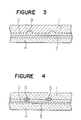
- Figure 3 is an enlarged view of portion B of Figure 1.
- Figure 4 is a diagrammatical cross-sectional view of another embodiment of portion B after recording.
- Figures 5 to 7 are waveform views showing output waveforms obtained by playing back optical discs prepared in Examples by a commercially available CD player.
- Figures 1 to 3 diagrammatically illustrate a structure of the optical information recording medium according to the present invention.
- reference numeral 1 indicates a light transmitting substrate
- numeral 2 indicates a light absorptive layer formed thereon, which generates heat upon absorption of an irradiated laser beam and is thereby melted, evaporated, sublimed, deformed or modified to form pits on the surface of the substrate 1 or in the light absorptive layer 2.
- Reference numeral 3 is a light reflective layer formed thereon
- numeral 4 indicates a protective layer provided thereon.
- the light transmitting substrate 1 is made of a material having high transparency to laser beams and is usually made of a resin having excellent strength such as a polycarbonate, an acrylate resin or an epoxy resin.
- the substrate may be made of any other material so long as it is transparent to writing and reading laser beams and at least the surface layer adjacent to the light absorptive layer 2 in the information recordable region 7 is deformable by energy generated by the light absorptive layer upon absorption of the writing laser beam, to form optically readable pits.
- the substrate or at least the surface layer thereof preferably has a heat distortion temperature within a range of from 85 to 200°C, more preferably from 90 to 150°C, as measured in accordance with ASTM D648 under a load of 4.6 kg/cm 2 and/or a Rockwell hardness within a range of from M200 to M75, more preferably from M105 to M80, as measured in accordance with ASTM D785.
- the heat distortion temperature or the Rockwell hardness of the substrate When the heat distortion temperature or the Rockwell hardness of the substrate is within the above-mentioned range, the energy generated by the light absorptive layer 2 upon absorption of the writing laser beam can effectively be absorbed by the local deformation of the surface layer of the substrate 1 so that no substantial strain will remain in the formed pits, whereby the stability of the recorded data will be secured. If the heat deformation temperature or the hardness is too low, the formed pits tend to easily be deformed by heat or external force, whereby the stability will be poor.
- the heat distortion temperature or the hardness is too high, the energy generated by the light absorptive layer 2 can hardly be absorbed in the form of deformation of the substrate 1, and it is difficult to form distinct pits 5, whereby it will be difficult to obtain read-out signals having a high degree of modulation.
- the thickness of the substrate 1 is not critical, but it is usually within a range of from 1.1 to 1.5 mm.
- the light absorptive layer 2 in the information recordable region 7 is a layer which absorbs a laser beam entered through the light transmitting substrate 1, whereupon it generates heat and at the same time undergoes melting, evaporation, sublimation, reaction, decomposition or modification. It is formed usually by spin coating a dye material such as a cyanine dye on the substrate 1.
- the light absorptive layer 2 may be formed to cover also the ROM region 6.
- the thickness of the light absorptive layer 2 is usually within a range of from 20 to 500 nm, preferably from 100 to 300 nm.
- the light reflective layer 3 is usually made of a metal such as gold, silver, copper, aluminum or an alloy thereof.
- the thickness of the light reflective layer 3 is usually within a range of from 30 to 150 nm, preferably from 40 to 130 nm.
- the protective layer 4 is made of a resin excellent in the impact resistance like the light transmitting substrate 1 and is most commonly formed by coating a ultraviolet curable resin by spin coating, followed by irradiation with ultraviolet rays for curing.
- a resin excellent in the impact resistance like the light transmitting substrate 1 is most commonly formed by coating a ultraviolet curable resin by spin coating, followed by irradiation with ultraviolet rays for curing.
- an epoxy resin, an acrylate resin and a silicone hard coat resin may usually be used.
- a resilient material such as a urethane resin to obtain a cushion effect.
- the thickness of the protective layer 4 is not critical and is usually within a range of from 3 to 30 ⁇ m, preferably from 5 to 15 ⁇ m.
- an organic dye to form the light absorptive layer 0.65 g of 1,1'-dibutyl-3,3,3',3'-tetramethyl-4,5,4',5'-dibenzoindodicarbocyanine perchlorate (product number NK3219, manufactured by Nippon Kanko Shikiso K.K.) was dissolved in 10 me of a diacetone alcohol solvent. The solution was coated by spin coating on the surface of the portion corresponding to the outer region of the substrate 1 i.e. the information recordable region 7 outside the diameter of 80 mm, to form a light absorptive layer 2 of a light sensitive dye film having a thickness of 0.13 ⁇ m.
- a gold film having a thickness of 400 ⁇ was formed by sputtering over the entire surface of a region of the diameter of from 45 to 118 mm of this disc, to form a light reflective layer 3.
- An ultraviolet curable resin was further spin-coated on this light reflective layer 3 and cured by irradiation with ultraviolet rays to form a protective layer 4 having a thickness of 10 ⁇ m.
- a semiconductor laser beam having a wavelength of 780 nm was irradiated at a linear speed of 1.2 m/sec with a recording power of 6.0 mW to record EFM signals.
- the CD standards prescribe that the reflectance is at least 70%, I 11 /I top is at least 0.6 and I 3 /I top is from 0.3 to 0.7.
- the optical disc of this example meets these standards with both the ROM region and the information recordable region.
- a gold film having a thickness of 400 ⁇ was formed by sputtering on the entire surface of a region of the diameter of from 45 to 118 mm of this disc, to form a light reflective layer 3.
- a semiconductor laser beam having a wavelength of 780 nm was irradiated at a linear speed of 1.2 m/sec with a recording power of 6.0 mW to record EFM signals. Then, this optical disc was played back by the same CD player as used in Example 1, whereby the waveform of the read-out signals obtained from the inside ROM region 6 was as shown in Figure 5, and in this region, the reflectance of the semiconductor laser beam was 85%, I 11 /I top was 0.7 and I 3 /I top was 0.47. Further, the waveform of the read-out signals obtained from the outside information recordable region 7 was as shown in Figure 7, and in this region, the reflectance of the semiconductor laser beam was 76%, I 11 /I top was 0.65 and I 3 /I top was 0.35.
- the CD standards prescribe that the reflectance is at least 70%' I 11 /I top is at least 0.6 and I 3 /I top is from 0.3 to 0.7.
- the optical disc of this example meets the standards with both the ROM region and the information recordable region.
- a gold film having a thickness of 400 ⁇ was formed by sputtering on the entire surface of a region of the diameter of from 45 to 118 mm of this disc, to form a light reflective layer 3.
- a semiconductor laser beam having a wavelength of 780 nm was irradiated at a linear speed of 1.2 m/sec with a recording power of 6.0 mW, to record EFM signals. Then, this optical disc was played back by the same CD player as used in Example 1, whereby the waveforms of the read-out signals, the reflectance of the semiconductor laser beam, I 11 /I top and I 3 /I top in both the inside ROM regions 6 and the information recordable regions 7, were substantially the same as in Example 2.
- a shock absorbing portion such as a space is formed behind the information recordable layer so that when the recording layer absorbs a laser beam and generates heat and is thereby melted, evaporated, sublimed, deformed or modified, such thermal changes are absorbed by the above shock absorbing portion, whereby pits are formed to the recording layer itself.
- the optical information recording medium of the present invention has a light reflective layer 3 behind the light absorptive layer 2 and a protective layer 4 behind the light reflective layer 3, and by forming the layers behind the light absorptive layer 2 with materials more hardly heat-deformable than the substrate 1, it is possible to employ a recording system wherein the thermal changes of the light absorptive layer 2 are absorbed by the substrate 1 so that optically modified pits such as protuberances, waved pits or dents will be formed on the substrate.
- the polycarbonate substrate 1 had a Rockwell hardness (ASTM D785) of M75 and a heat distortion temperature (ASTM D648) of 132°C under a load of 4.6 kg/cm 2 .
- the protective layer 4 had a Rockwell hardness (ASTM D785) of M90 and a heat distortion temperation (ASTM D648) of 150°C under a load of 4.6 kg/cm 2 .
- the protective layer 4 behind the light absorptive layer 2 is made of a material more hardly heat-deformable than the substrate, whereby the thermal changes of the light absorptive layer 2 are absorbed by the surface of the substrate 1 and pits in the form of protuberances are formed on the surface of the substrate.
- pits 5 in the form of protuberances are observed on the surface of the substrate 1 of the optical disc which is in contact with the light absorptive layer 2.
- the optical information recording medium of the present invention has a ROM region and an information recordable region on the same medium, whereby at the ROM region, the same data can be recorded in a large quantity and the recorded data can be reproduced without inadvertent erasure, and at the same time, in the information recordable region, the user can record any optional data.
- the optical information recording medium of the present invention is useful for wide a range of applications.
Abstract
Description
- The present invention relates to an optical information recording medium of the type wherein recorded data are reproduced by scanning them by a laser beam More particularly, it relates to an optical information recording medium comprising a ROM region where data are already recorded and an information recordable region where data can be recorded.
- Conventional so-called writable optical information recording media capable of recording data by means of laser beams, have a recording layer of e.g. a metal such as Te, Bi or Mn or a dye such as cyanine, merocyanine or phthalocyanine, and they are designed to record data in such a manner that when irradiated with a laser beam, such recording layer is deformed, sublimed, evaporated or modified to form pits. With optical information recording media having such recording layer, it is common to form a space behind the recording layer to facilitate the deformation, sublimation, evaporation or modification of the recording layer for the formation of the pits. A typical example is a laminated structure so-called an air sandwich structure wherein a pair of substrates are laminated with a space therebetween.
- With the optical information recording media of this type, a writing laser beam is irradiated through a transparent substrate to form optically readable pits in the recording layer. For reproducing the recorded data, a reading laser beam having a less power than the writing laser beam is irradiated through the substrate, and the contrast between the light reflected from the pits and the light reflected from non-pitted portion, is read as an electrical signal.
- On the other hand, optical information recording media of so-called ROM (read only memory) type wherein data are already recorded, and no further data are recordable or the recorded data are no longer erasable or rewritable, are widely practically employed in the sound recording and information treating fields. Optical information recording media of this type have no such a recording layer as described above. Prepits or pregrooves corresponding to data to be reproduced are already formed on a substrate of e.g. polycarbonate by e.g. press molding, a reflective layer of a metal such as Au, Ag, Cu or Al is formed thereon, and a protective layer is further provided thereon.
- The most typical optical information recording medium of this ROM type is a compact disc so-called CD which is widely used in the sound recording and information treating fields. The specification for recording and read-out signals for this CD is standardized, and the reproducing or play back apparatus for CD in accordance with this standard is widely available as compact disc players (CD players).
- The above-mentioned optical information recording media all take a disc form having a center hole for engagement with a rotatory shaft, i.e. a form of an optical disc.
- Heretofore, such recordable optical information recording media and ROM type optical information recording media have been available as separate media independently.
- ROM type optical information recording media have a merit in that media having the same data can be produced in a large quantity, and the recorded data will not be erased inadvertently. However, the user can not record optional data thereon.
- On the other hand, in the case of recordable optical information recording media, the user can record any optional data thereon. However, such recording media are not suitable for recording the same data in a large quantity, and they also have a demerit that the recorded data may inadvertently be erased.
- In view of the respective characteristics, their uses are naturally different from each other. Thus, conventional optical information recording media are restricted in use for one of the two types of applications.
- Under the circumstances, it is an object of the present invention to solve such conventional problems and to provide an optical information recording medium having both a recordable region and a ROM region.
- Namely, the present invention provides an optical information recording medium of the type wherein recorded data are reproduced by scanning them with a laser beam, which comprises a ROM region where optically readable pits are already formed and an information recordable region where optically readable pits can be formed by irradiation with a writing laser beam, wherein the information recordable region comprises a light transmitting substrate having a deformable surface, a light absorptive layer overlaying the deformable surface, to absorb the writing laser beam, and a light reflective layer overlaying the light absorptive layer, said deformable surface being deformable by energy generated upon absorption of the writing laser beam by the light absorptive layer, to form optically readable pits.
- The optical information recording medium of the present invention has an information recordable region and a ROM region on a single substrate, whereby in the ROM region, the same data can be recorded in a large quantity by e.g. press molding and there is no danger of inadvertent erasure of the recorded data, and in the recordable region, any desired data may be recorded at will by the user.
- Further, in a case where a light absorptive layer is formed on the substrate by coating, such a light absorptive layer may be formed to fill up the pregroove formed preliminarily on the substrate, so that the attenuation of light due to interference of the light reflected from the pregroove and the light reflected from the land will be suppressed, whereby the reflectance for reproduction at the pregroove portion will be high, and the degree of modulation of pits formed in the information recordable region can be made high. Thus, the read-out signals from the pits formed in the information recordable region and the read-out signals from the prepits on the substrate will both have adequate degrees of modulation.
- Now, the preferred embodiments of the present invention will be described in detail with reference to the drawings, in which:
- Figure 1 is a partially cross-sectional perspective view diagrammatically illustrating one embodiment of the structure of the optical information recording medium of the present invention.
- Figure 2 is an enlarged view of portion of Figure 1.
- Figure 3 is an enlarged view of portion B of Figure 1.
- Figure 4 is a diagrammatical cross-sectional view of another embodiment of portion B after recording.
- Figures 5 to 7 are waveform views showing output waveforms obtained by playing back optical discs prepared in Examples by a commercially available CD player.
- Figures 1 to 3 diagrammatically illustrate a structure of the optical information recording medium according to the present invention. In these Figures, reference numeral 1 indicates a light transmitting substrate, and
numeral 2 indicates a light absorptive layer formed thereon, which generates heat upon absorption of an irradiated laser beam and is thereby melted, evaporated, sublimed, deformed or modified to form pits on the surface of the substrate 1 or in the lightabsorptive layer 2.Reference numeral 3 is a light reflective layer formed thereon, andnumeral 4 indicates a protective layer provided thereon. - The light transmitting substrate 1 is made of a material having high transparency to laser beams and is usually made of a resin having excellent strength such as a polycarbonate, an acrylate resin or an epoxy resin. However, the substrate may be made of any other material so long as it is transparent to writing and reading laser beams and at least the surface layer adjacent to the light
absorptive layer 2 in the informationrecordable region 7 is deformable by energy generated by the light absorptive layer upon absorption of the writing laser beam, to form optically readable pits. In this respect, the substrate or at least the surface layer thereof preferably has a heat distortion temperature within a range of from 85 to 200°C, more preferably from 90 to 150°C, as measured in accordance with ASTM D648 under a load of 4.6 kg/cm2 and/or a Rockwell hardness within a range of from M200 to M75, more preferably from M105 to M80, as measured in accordance with ASTM D785. When the heat distortion temperature or the Rockwell hardness of the substrate is within the above-mentioned range, the energy generated by the lightabsorptive layer 2 upon absorption of the writing laser beam can effectively be absorbed by the local deformation of the surface layer of the substrate 1 so that no substantial strain will remain in the formed pits, whereby the stability of the recorded data will be secured. If the heat deformation temperature or the hardness is too low, the formed pits tend to easily be deformed by heat or external force, whereby the stability will be poor. On the other hand, if the heat distortion temperature or the hardness is too high, the energy generated by the lightabsorptive layer 2 can hardly be absorbed in the form of deformation of the substrate 1, and it is difficult to formdistinct pits 5, whereby it will be difficult to obtain read-out signals having a high degree of modulation. - The thickness of the substrate 1 is not critical, but it is usually within a range of from 1.1 to 1.5 mm.
- The light
absorptive layer 2 in the informationrecordable region 7 is a layer which absorbs a laser beam entered through the light transmitting substrate 1, whereupon it generates heat and at the same time undergoes melting, evaporation, sublimation, reaction, decomposition or modification. It is formed usually by spin coating a dye material such as a cyanine dye on the substrate 1. The lightabsorptive layer 2 may be formed to cover also the ROM region 6. - The thickness of the light
absorptive layer 2 is usually within a range of from 20 to 500 nm, preferably from 100 to 300 nm. - The light
reflective layer 3 is usually made of a metal such as gold, silver, copper, aluminum or an alloy thereof. The thickness of the lightreflective layer 3 is usually within a range of from 30 to 150 nm, preferably from 40 to 130 nm. - The
protective layer 4 is made of a resin excellent in the impact resistance like the light transmitting substrate 1 and is most commonly formed by coating a ultraviolet curable resin by spin coating, followed by irradiation with ultraviolet rays for curing. As other materials, an epoxy resin, an acrylate resin and a silicone hard coat resin may usually be used. It is also possible to employ a resilient material such as a urethane resin to obtain a cushion effect. - The thickness of the
protective layer 4 is not critical and is usually within a range of from 3 to 30 µm, preferably from 5 to 15 µm. - Now, specific Examples of this structure will be described.
- A polycarbonate substrate 1 of a disc shape having a thickness of 1.2 mm, an outer diameter of 120 mm and an inner diameter of 15 mm and having a
spiral prepit 8 capable of reproducing CD format signals formed with a width of 0.6 µm, a depth of 0.08 µm and a pitch of 1.6 pm in a range (ROM region 6) of the diameter of from 46 to 80 mm and having a spiral pregroove 9 (tracking guide groove) formed with a width of 0.8 µm, a depth of 0.08 µm and a pitch of 1.6 µm in a range (information recordable region 7) of the diameter of 80 to 117 mm outside the ROM region 6, was formed by injection molding. - As an organic dye to form the light absorptive layer, 0.65 g of 1,1'-dibutyl-3,3,3',3'-tetramethyl-4,5,4',5'-dibenzoindodicarbocyanine perchlorate (product number NK3219, manufactured by Nippon Kanko Shikiso K.K.) was dissolved in 10 me of a diacetone alcohol solvent. The solution was coated by spin coating on the surface of the portion corresponding to the outer region of the substrate 1 i.e. the information
recordable region 7 outside the diameter of 80 mm, to form a lightabsorptive layer 2 of a light sensitive dye film having a thickness of 0.13 µm. - Then, a gold film having a thickness of 400 Å was formed by sputtering over the entire surface of a region of the diameter of from 45 to 118 mm of this disc, to form a light
reflective layer 3. An ultraviolet curable resin was further spin-coated on this lightreflective layer 3 and cured by irradiation with ultraviolet rays to form aprotective layer 4 having a thickness of 10 µm. To the informationrecordable region 7 of the optical disc thus obtained, a semiconductor laser beam having a wavelength of 780 nm was irradiated at a linear speed of 1.2 m/sec with a recording power of 6.0 mW to record EFM signals. Then, this optical disc was played back by a commercially available CD player (Aurex XR-V73, wavelength of the reading laser beam λ=780 nm), whereby the waveform of the read-out signals obtained from the inside ROM region 6 was as shown in Figure 5, and in this region, the reflectance of the semiconductor laser beam was 85%, I11/Itop was 0.7 and I3/Itop was 0.47. Further, the waveform of the read-out signals obtained from the outside informationrecordable region 7 was as shown in Figure 6, and in this region, the reflectance of the semiconductor laser beam was 72%, I11/Itop was 0.65 and I3/Itop was 0.35. - The CD standards prescribe that the reflectance is at least 70%, I11/Itop is at least 0.6 and I3/Itop is from 0.3 to 0.7. The optical disc of this example meets these standards with both the ROM region and the information recordable region.
- A polycarbonate substrate 1 of a disc shape having a thickness of 1.2 mm, an outer diameter of 120 mm and an inner diameter of 15 mm and having a
spiral prepit 8 capable of reproducing CD format signals formed with a width of 0.6 µm, a depth of 0.08 µm and a pitch of 1.6 µm in a range (ROM region 6) of the diameter of from 46 to 100 mm and having aspiral pregroove 9 formed with a width of 0.6 µm, a depth of 0.08 µm and a pitch of 1.6 µm in a range (information recordable region 7) of the diameter of from 100 to 117 mm outside the ROM region 6, was formed by injection molding. - The portion inward from the diameter of 100 mm of the substrate i.e. the ROM region 6, was masked, and a GaAs film having a thickness of 900 Å was formed by sputtering on the outer circumferential portion i.e. the information
recordable region 7, to form a lightabsorptive layer 2. - A gold film having a thickness of 400 Å was formed by sputtering on the entire surface of a region of the diameter of from 45 to 118 mm of this disc, to form a light
reflective layer 3. - To the information
recordable region 7 of the optical disc thus obtained, a semiconductor laser beam having a wavelength of 780 nm was irradiated at a linear speed of 1.2 m/sec with a recording power of 6.0 mW to record EFM signals. Then, this optical disc was played back by the same CD player as used in Example 1, whereby the waveform of the read-out signals obtained from the inside ROM region 6 was as shown in Figure 5, and in this region, the reflectance of the semiconductor laser beam was 85%, I11/Itop was 0.7 and I3/Itop was 0.47. Further, the waveform of the read-out signals obtained from the outside informationrecordable region 7 was as shown in Figure 7, and in this region, the reflectance of the semiconductor laser beam was 76%, I11/Itop was 0.65 and I3/Itop was 0.35. - The CD standards prescribe that the reflectance is at least 70%' I11/Itop is at least 0.6 and I3/Itop is from 0.3 to 0.7. The optical disc of this example meets the standards with both the ROM region and the information recordable region.
- A polycarbonate substrate 1 of a disc shape having a thickness of 1.2 mm, an outer diameter of 120 mm and an inner diameter of 15 mm and having a
spiral prepit 8 capable of reproducing CD format signals formed with a width of 0.5 µm, a depth of 0.08 µm and a pitch of 1.6 µm in ranges (ROM regions 6) of the diameters of from 46 to 70 mm and from 85 to 102 mm and having aspiral pregroove 9 formed with a width of 0.6 µm, a depth of 0.08 µm and a pitch of 1.6 µm in ranges (information recordable regions 7) of the diameter of from 70 to 85 mm therebetween and from 102 to 117 mm outside thereof, was formed by injection molding. - The portions corresponding to the ranges of the diameter of from 46 to 70 mm and from 85 to 102 mm, i.e. the ROM regions 6, were masked, and a GaAs film having a thickness of 900 Å was formed on the remaining portion i.e. the information
recordable region 7, to form a lightabsorptive layer 2. - A gold film having a thickness of 400 Å was formed by sputtering on the entire surface of a region of the diameter of from 45 to 118 mm of this disc, to form a light
reflective layer 3. - To the information
recordable regions 7 of the optical disc thus obtained, a semiconductor laser beam having a wavelength of 780 nm was irradiated at a linear speed of 1.2 m/sec with a recording power of 6.0 mW, to record EFM signals. Then, this optical disc was played back by the same CD player as used in Example 1, whereby the waveforms of the read-out signals, the reflectance of the semiconductor laser beam, I11/Itop and I3/Itop in both the inside ROM regions 6 and the informationrecordable regions 7, were substantially the same as in Example 2. - In conventional information recording media, it is common that a shock absorbing portion such as a space is formed behind the information recordable layer so that when the recording layer absorbs a laser beam and generates heat and is thereby melted, evaporated, sublimed, deformed or modified, such thermal changes are absorbed by the above shock absorbing portion, whereby pits are formed to the recording layer itself. Whereas, the optical information recording medium of the present invention has a light
reflective layer 3 behind the lightabsorptive layer 2 and aprotective layer 4 behind the lightreflective layer 3, and by forming the layers behind the lightabsorptive layer 2 with materials more hardly heat-deformable than the substrate 1, it is possible to employ a recording system wherein the thermal changes of the lightabsorptive layer 2 are absorbed by the substrate 1 so that optically modified pits such as protuberances, waved pits or dents will be formed on the substrate. - For example, in the above Example 1, the polycarbonate substrate 1 had a Rockwell hardness (ASTM D785) of M75 and a heat distortion temperature (ASTM D648) of 132°C under a load of 4.6 kg/cm2. Whereas, after curing the
protective layer 4 had a Rockwell hardness (ASTM D785) of M90 and a heat distortion temperation (ASTM D648) of 150°C under a load of 4.6 kg/cm2. Namely, in the optical information recording medium of this Example, theprotective layer 4 behind the lightabsorptive layer 2 is made of a material more hardly heat-deformable than the substrate, whereby the thermal changes of the lightabsorptive layer 2 are absorbed by the surface of the substrate 1 and pits in the form of protuberances are formed on the surface of the substrate. Thus, as shown diagrammatically in Figure 4, after the recording, pits 5 in the form of protuberances are observed on the surface of the substrate 1 of the optical disc which is in contact with the lightabsorptive layer 2. - As described in the foregoing, the optical information recording medium of the present invention has a ROM region and an information recordable region on the same medium, whereby at the ROM region, the same data can be recorded in a large quantity and the recorded data can be reproduced without inadvertent erasure, and at the same time, in the information recordable region, the user can record any optional data. Thus, the optical information recording medium of the present invention is useful for wide a range of applications.
Claims (4)
- An optical information recording medium of the type wherein recorded data can be reproduced by scanning them with a laser beam which comprisesan optically readable region andan information recordable region where optically readable pits can be formed by irradiation with a writing laser beam,characterized in thatthe medium comprises a light-transmitting substrate having a deformable surface and a light-reflective layer overlaying the deformable surface andin that the information recordable region additionally comprises a light-absorptive layer between the deformable surface and the light-reflective layer for absorbing the writing laser beam,whereby energy is generated so as to form optically readable pits on the deformable surface,and when the deformable surface is irradiated by laser beam, the light-absorptive layer is able to change the optical character,and the optically readable region comprises a light-transmitting substrate and a light-reflective layer overlaying the light-transmitting substrateand in that the optically readable region additionally comprises a light-absorptive layer between the light-transmitting substrate and the light-reflective layer.
- The optical information recording medium according to claim 1, wherein the optical character of the light-absorptive layer is a refractive index.
- The optical information recording medium according to claim 1 or 2, wherein the change of the optical character of the light-absorptive layer is caused by melting, evaporation, sublimation, decomposition or modification.
- The optical information recording medium according to claim 1 or 2, wherein the change of the optical character of the light-absorptive layer is an apparent darkness of a pit.
Applications Claiming Priority (10)
| Application Number | Priority Date | Filing Date | Title |
|---|---|---|---|
| JP191715/88 | 1988-07-30 | ||
| JP19171688 | 1988-07-30 | ||
| JP19171588 | 1988-07-30 | ||
| JP63191715A JPH07114028B2 (en) | 1988-07-30 | 1988-07-30 | Optical information recording medium |
| JP191716/88 | 1988-07-30 | ||
| JP19171688 | 1988-07-30 | ||
| JP751189 | 1989-01-14 | ||
| JP1007511A JPH0827985B2 (en) | 1988-07-30 | 1989-01-14 | Optical information recording medium and its recording method |
| JP7511/89 | 1989-01-14 | ||
| EP19890106809 EP0353391B1 (en) | 1988-07-30 | 1989-04-17 | Optical information recording medium |
Related Parent Applications (2)
| Application Number | Title | Priority Date | Filing Date |
|---|---|---|---|
| EP89106809.0 Division | 1989-04-17 | ||
| EP19890106809 Division EP0353391B1 (en) | 1988-07-30 | 1989-04-17 | Optical information recording medium |
Publications (3)
| Publication Number | Publication Date |
|---|---|
| EP0741383A2 true EP0741383A2 (en) | 1996-11-06 |
| EP0741383A3 EP0741383A3 (en) | 1996-11-20 |
| EP0741383B1 EP0741383B1 (en) | 2002-07-03 |
Family
ID=27277632
Family Applications (2)
| Application Number | Title | Priority Date | Filing Date |
|---|---|---|---|
| EP19890106809 Expired - Lifetime EP0353391B1 (en) | 1988-07-30 | 1989-04-17 | Optical information recording medium |
| EP19960112240 Expired - Lifetime EP0741383B1 (en) | 1988-07-30 | 1989-04-17 | Optical information recording medium |
Family Applications Before (1)
| Application Number | Title | Priority Date | Filing Date |
|---|---|---|---|
| EP19890106809 Expired - Lifetime EP0353391B1 (en) | 1988-07-30 | 1989-04-17 | Optical information recording medium |
Country Status (9)
| Country | Link |
|---|---|
| US (1) | US4940618A (en) |
| EP (2) | EP0353391B1 (en) |
| KR (1) | KR950005035B1 (en) |
| AT (2) | ATE220238T1 (en) |
| CA (1) | CA1320573C (en) |
| DE (2) | DE68929413T2 (en) |
| ES (2) | ES2179137T3 (en) |
| HK (1) | HK1000262A1 (en) |
| SG (1) | SG43846A1 (en) |
Families Citing this family (56)
| Publication number | Priority date | Publication date | Assignee | Title |
|---|---|---|---|---|
| US5155723A (en) * | 1988-07-30 | 1992-10-13 | Yuden Co., Ltd. Taiyo | Optical information recording method and medium |
| US5249175A (en) * | 1988-09-09 | 1993-09-28 | Matsushita Electric Industrial Co., Ltd. | Optical information recording medium and information recording and reproducing method therefor |
| JP2760812B2 (en) * | 1988-09-28 | 1998-06-04 | 株式会社日立製作所 | Optical reproducing apparatus and optical reproducing method |
| US5075147A (en) * | 1989-03-24 | 1991-12-24 | Fuji Photo Film Co., Ltd. | Method for optically recording information and information recorded medium |
| JPH0827983B2 (en) | 1989-05-02 | 1996-03-21 | 太陽誘電株式会社 | Optical information recording medium |
| JPH0383226A (en) * | 1989-08-25 | 1991-04-09 | Sony Corp | Recording medium |
| JP2600004B2 (en) * | 1990-02-06 | 1997-04-16 | シャープ株式会社 | Magneto-optical recording medium and surface treatment method thereof |
| US5336531A (en) * | 1990-02-06 | 1994-08-09 | Sharp Kabushiki Kaisha | Magneto-optical disk and manufacturing methods thereof |
| US5204852A (en) * | 1990-02-17 | 1993-04-20 | Victor Company Of Japan, Ltd. | Optical disc-like recoding medium and manufacturing method thereof |
| JPH03275382A (en) * | 1990-03-27 | 1991-12-06 | Fuji Photo Film Co Ltd | Optical recording medium and recording regeneration method |
| CA2044427C (en) * | 1990-06-13 | 1997-02-11 | Junichiro Nakayama | Magneto-optical disk and manufacturing methods thereof |
| JP3126411B2 (en) * | 1990-06-22 | 2001-01-22 | 三井化学株式会社 | Optical recording medium and recording method |
| US5274623A (en) * | 1990-07-19 | 1993-12-28 | Fuji Photo Film Co., Ltd. | Information recording medium having high modulation degree |
| GB9017266D0 (en) * | 1990-08-07 | 1990-09-19 | Ici Plc | Optical recording elements |
| JPH0497242A (en) * | 1990-08-10 | 1992-03-30 | Sharp Corp | Information recording and reproducing method |
| NL9002024A (en) * | 1990-09-14 | 1992-04-01 | Philips Nv | OPTICAL REGISTRATION ELEMENT. |
| US5401549A (en) * | 1990-10-15 | 1995-03-28 | Ricoh Company, Ltd. | Optical information recording medium |
| JP3109866B2 (en) * | 1990-11-17 | 2000-11-20 | 太陽誘電株式会社 | Substrate for optical information recording carrier and method of manufacturing the same |
| US5316814A (en) * | 1991-05-14 | 1994-05-31 | Ricoh Company, Ltd. | Optical information recording medium |
| JPH05579A (en) * | 1991-06-25 | 1993-01-08 | Pioneer Electron Corp | Optical recording medium |
| JP3160632B2 (en) * | 1991-09-27 | 2001-04-25 | ソニー株式会社 | Optical disc and its reproducing method |
| US5272047A (en) * | 1992-06-26 | 1993-12-21 | Eastman Kodak Company | Optical information recording medium using azo dyes |
| CA2110233C (en) | 1992-12-02 | 1999-01-12 | Mitsui Toatsu Chemicals, Incorporated | Optical information recording medium and composition for optical information recording film |
| US6168901B1 (en) | 1993-01-08 | 2001-01-02 | Eastman Kodak Company | Recordable optical element using low absorption materials |
| US5294471A (en) * | 1993-02-01 | 1994-03-15 | Eastman Kodak Company | Optical information recording medium using metallized formazan dyes |
| US5362536A (en) * | 1993-02-19 | 1994-11-08 | Eastman Kodak Company | Recordable optical element having a leuco dye |
| US5356685A (en) * | 1993-02-19 | 1994-10-18 | Eastman Kodak Company | Recordable optical element having a leuco dye |
| US5326677A (en) * | 1993-02-19 | 1994-07-05 | Eastman Kodak Company | Optical retrieval apparatus using a tellurium (IV) leuco dye |
| JP3145235B2 (en) * | 1993-09-03 | 2001-03-12 | パイオニア株式会社 | Recordable disc, recording device and recording method thereof |
| US5426015A (en) * | 1993-10-18 | 1995-06-20 | Eastman Kodak Company | Metallized azo dianion with two cationic dye counter ions for optical information recording medium |
| US5518789A (en) | 1994-05-17 | 1996-05-21 | Eastman Kodak Company | Thioether containing photopolymerizable compositions |
| US5547728A (en) * | 1994-09-23 | 1996-08-20 | Eastman Kodak Company | Optical recording elements having recording layers containing mixtures of formazan and cyanine dyes |
| US5547727A (en) * | 1994-12-13 | 1996-08-20 | Eastman Kodak Company | Optical recording elements having recording layers containing cationic azo dyes |
| US5470626A (en) * | 1995-02-21 | 1995-11-28 | Eastman Kodak Company | Optical recording layers containing sulfur |
| US5585158A (en) * | 1995-06-07 | 1996-12-17 | Eastman Kodak Company | Recordable optical element using low absorption materials |
| US5667860A (en) | 1995-11-14 | 1997-09-16 | Eastman Kodak Company | Optical recording elements having recording layers exhibiting reduced bubble formation |
| US5728441A (en) * | 1995-12-01 | 1998-03-17 | Samsung Electronics Co., Ltd. | Recordable/replayable optical recording medium and optical recording method therefor |
| US5925433A (en) * | 1995-12-01 | 1999-07-20 | Akzo Nobel N.V. | Optical recording medium based on Fabry-Perot principle |
| US5725741A (en) * | 1996-04-12 | 1998-03-10 | Eastman Kodak Company | Method of forming recordable optical element using low absorption materials |
| US5770293A (en) * | 1996-04-12 | 1998-06-23 | Eastman Kodak Company | Method of forming recordable optical element using low absorption materials |
| CN1233339A (en) * | 1996-09-02 | 1999-10-27 | 阿克佐诺贝尔公司 | Optical recording medium comprising a cross-linked buffer layer |
| US5695843A (en) * | 1996-09-27 | 1997-12-09 | Eastman Kodak Company | Mixtures of symmetrical and unsymmetrical nickel formazan dyes |
| KR100230448B1 (en) * | 1996-10-10 | 1999-11-15 | 윤종용 | Optical recording medium |
| KR100230449B1 (en) * | 1996-10-10 | 1999-11-15 | 윤종용 | Optical recording medium |
| US5963536A (en) * | 1997-04-08 | 1999-10-05 | Eastman Kodak Company | Copy count protection structure for optical recording medium and method for same |
| US6007887A (en) * | 1997-12-15 | 1999-12-28 | Eastman Kodak Company | Performance recording media for recordable element using silver reflector |
| US6020041A (en) * | 1997-12-15 | 2000-02-01 | Eastman Kodak Company | Performance recording media for recordable element using gold reflector |
| JP3697896B2 (en) | 1998-01-23 | 2005-09-21 | 株式会社デンソー | Optical information recording medium and manufacturing method thereof |
| US6228440B1 (en) | 1998-07-28 | 2001-05-08 | Motorola, Inc. | Perishable media information storage mechanism and method of fabrication |
| US6242068B1 (en) | 1999-12-28 | 2001-06-05 | Eastman Kodak Company | Recordable optical media with a silver-palladium reflective layer |
| US6638593B2 (en) | 2000-06-30 | 2003-10-28 | Verification Technologies, Inc. | Copy-protected optical media and method of manufacture thereof |
| US20030117936A1 (en) * | 2001-12-20 | 2003-06-26 | Eastman Kodak Company | Hybrid disc architecture |
| JP4273705B2 (en) * | 2002-05-13 | 2009-06-03 | 日本電気株式会社 | Optical disc media |
| JP4782189B2 (en) * | 2006-03-03 | 2011-09-28 | シャープ株式会社 | Optical information recording medium and reproducing apparatus |
| WO2009028593A1 (en) | 2007-08-30 | 2009-03-05 | Sharp Kabushiki Kaisha | Super-resolution optical recording medium, optical recording medium reproduction device, control method of optical recording medium reproduction device, control program for optical recording medium reproduction device, and computer readable medium for recording the program |
| CN112002782B (en) * | 2020-08-28 | 2022-03-01 | 河南师范大学 | Based on MnBi2Te4Single-layer nanoscale photoelectric sensor |
Citations (6)
| Publication number | Priority date | Publication date | Assignee | Title |
|---|---|---|---|---|
| FR2441237A1 (en) * | 1978-11-08 | 1980-06-06 | Philips Nv | RECORDING CARRIER IN WHICH INFORMATION CAN BE RECORDED OPTICALLY |
| JPS5919253A (en) * | 1982-07-23 | 1984-01-31 | Sony Corp | Information recording medium |
| EP0132410A2 (en) * | 1983-07-25 | 1985-01-30 | Sony Corporation | Information recording media |
| JPS62137744A (en) * | 1985-12-11 | 1987-06-20 | Hitachi Ltd | Optical disk |
| JPS62246786A (en) * | 1986-04-21 | 1987-10-27 | Canon Inc | Optical recording medium |
| JPS62246782A (en) * | 1986-04-21 | 1987-10-27 | Canon Inc | Optical recording medium |
Family Cites Families (10)
| Publication number | Priority date | Publication date | Assignee | Title |
|---|---|---|---|---|
| FR2368779A1 (en) * | 1976-10-22 | 1978-05-19 | Thomson Brandt | THERMOSENSITIVE MEDIA INTENDED FOR RECORDING INFORMATION AND PROCESS FOR RECORDING INFORMATION ON SUCH MEDIA |
| US4315269A (en) * | 1977-08-29 | 1982-02-09 | Rca Corporation | Thick protective overcoat layer for optical video disc |
| FR2474222A1 (en) * | 1980-01-23 | 1981-07-24 | Thomson Csf | METHOD FOR THERMO-OPTICAL INFORMATION REGISTRATION AND INFORMATION CARRIER FOR IMPLEMENTING SAID METHOD |
| FR2474223A1 (en) * | 1980-01-23 | 1981-07-24 | Thomson Csf | METHOD FOR THERMO-OPTICAL INFORMATION REGISTRATION AND INFORMATION CARRIER FOR IMPLEMENTING SAID METHOD |
| US4360908A (en) * | 1980-02-25 | 1982-11-23 | Eastman Kodak Company | Physically optimized optical disc structure, method and apparatus |
| DE3118058A1 (en) * | 1980-05-14 | 1982-03-11 | RCA Corp., 10020 New York, N.Y. | RECORD CARRIER AND METHOD FOR WRITING AN INFORMATION TRACK AND DELETING AN INFORMATION STORED IN THE CARRIER |
| FR2488711B1 (en) * | 1980-08-13 | 1985-06-28 | Thomson Csf | THERMO-OPTICAL INFORMATION RECORDING PROCESS AND INFORMATION MEDIUM FOR CARRYING OUT SAID METHOD |
| KR870002142B1 (en) * | 1982-09-20 | 1987-12-12 | 디스커비소젼 어시에이츠 | Optical recording medium and its making method |
| JPS62110636A (en) * | 1985-11-08 | 1987-05-21 | Kyodo Printing Co Ltd | Optical recording medium and its manufacture |
| JPH0734269B2 (en) * | 1986-10-23 | 1995-04-12 | 松下電器産業株式会社 | Optical recording medium |
-
1989
- 1989-04-14 US US07/340,078 patent/US4940618A/en not_active Expired - Lifetime
- 1989-04-17 EP EP19890106809 patent/EP0353391B1/en not_active Expired - Lifetime
- 1989-04-17 AT AT96112240T patent/ATE220238T1/en not_active IP Right Cessation
- 1989-04-17 SG SG1996002100A patent/SG43846A1/en unknown
- 1989-04-17 DE DE1989629413 patent/DE68929413T2/en not_active Expired - Lifetime
- 1989-04-17 ES ES96112240T patent/ES2179137T3/en not_active Expired - Lifetime
- 1989-04-17 ES ES89106809T patent/ES2097738T3/en not_active Expired - Lifetime
- 1989-04-17 EP EP19960112240 patent/EP0741383B1/en not_active Expired - Lifetime
- 1989-04-17 AT AT89106809T patent/ATE148803T1/en not_active IP Right Cessation
- 1989-04-17 DE DE1989627751 patent/DE68927751T2/en not_active Expired - Lifetime
- 1989-05-11 CA CA 599418 patent/CA1320573C/en not_active Expired - Lifetime
- 1989-07-22 KR KR1019890010427A patent/KR950005035B1/en not_active IP Right Cessation
-
1997
- 1997-09-16 HK HK97101791A patent/HK1000262A1/en not_active IP Right Cessation
Patent Citations (6)
| Publication number | Priority date | Publication date | Assignee | Title |
|---|---|---|---|---|
| FR2441237A1 (en) * | 1978-11-08 | 1980-06-06 | Philips Nv | RECORDING CARRIER IN WHICH INFORMATION CAN BE RECORDED OPTICALLY |
| JPS5919253A (en) * | 1982-07-23 | 1984-01-31 | Sony Corp | Information recording medium |
| EP0132410A2 (en) * | 1983-07-25 | 1985-01-30 | Sony Corporation | Information recording media |
| JPS62137744A (en) * | 1985-12-11 | 1987-06-20 | Hitachi Ltd | Optical disk |
| JPS62246786A (en) * | 1986-04-21 | 1987-10-27 | Canon Inc | Optical recording medium |
| JPS62246782A (en) * | 1986-04-21 | 1987-10-27 | Canon Inc | Optical recording medium |
Non-Patent Citations (5)
| Title |
|---|
| AHN K.Y. ET AL: 'deformed mirror optical storage structure' IBM TECHNICAL DISCLOSURE BULLETIN vol. 25, no. 11B, April 1983, ARMONK, USA, pages 5940 - 5941 * |
| PATENT ABSTRACTS OF JAPAN vol. 008, no. 109 (P-275), 22 May 1984 & JP-A-59 019253 (SONY KK), 31 January 1984, * |
| PATENT ABSTRACTS OF JAPAN vol. 011, no. 362 (P-640), 26 November 1987 & JP-A-62 137744 (HITACHI LTD), 20 June 1987, * |
| PATENT ABSTRACTS OF JAPAN vol. 012, no. 120 (M-685), 14 April 1988 & JP-A-62 246782 (CANON INC), 27 October 1987, * |
| PATENT ABSTRACTS OF JAPAN vol. 012, no. 120 (M-685), 14 April 1988 & JP-A-62 246786 (CANON INC), 27 October 1987, * |
Also Published As
| Publication number | Publication date |
|---|---|
| EP0353391A3 (en) | 1990-08-08 |
| KR910003605A (en) | 1991-02-27 |
| ES2179137T3 (en) | 2003-01-16 |
| EP0353391A2 (en) | 1990-02-07 |
| ES2097738T3 (en) | 1997-04-16 |
| US4940618A (en) | 1990-07-10 |
| KR950005035B1 (en) | 1995-05-17 |
| DE68929413D1 (en) | 2002-08-08 |
| EP0353391B1 (en) | 1997-02-05 |
| DE68927751T2 (en) | 1997-05-28 |
| DE68927751D1 (en) | 1997-03-20 |
| DE68929413T2 (en) | 2002-10-31 |
| EP0741383B1 (en) | 2002-07-03 |
| HK1000262A1 (en) | 1998-02-13 |
| ATE148803T1 (en) | 1997-02-15 |
| SG43846A1 (en) | 1997-11-14 |
| CA1320573C (en) | 1993-07-20 |
| ATE220238T1 (en) | 2002-07-15 |
| EP0741383A3 (en) | 1996-11-20 |
Similar Documents
| Publication | Publication Date | Title |
|---|---|---|
| EP0741383B1 (en) | Optical information recording medium | |
| US4990388A (en) | Optical information recording medium | |
| US5155723A (en) | Optical information recording method and medium | |
| EP0353393B2 (en) | Optical information recording medium | |
| US5204220A (en) | Optical recording medium | |
| KR100230448B1 (en) | Optical recording medium | |
| JP3026357B2 (en) | Optical recording medium | |
| JPH07114028B2 (en) | Optical information recording medium | |
| US5336584A (en) | Optical recording medium | |
| US5441848A (en) | Optical recording/reproducing method | |
| JP3548929B2 (en) | Optical information recording medium | |
| EP0777224B1 (en) | Optical recording medium and method | |
| US6521317B2 (en) | Optical recording medium | |
| KR100292378B1 (en) | Optical recording medium capable of performing recording/reproducing operations and optical recording method thereof | |
| EP1055232B1 (en) | Optical recording medium based on thin recording layers | |
| JP2834420B2 (en) | Optical information recording medium | |
| KR100207582B1 (en) | Optical recording medium | |
| KR19980022575A (en) | Recordable optical disc | |
| JP2793516B2 (en) | Optical information recording medium and reproducing method thereof | |
| KR100207581B1 (en) | Optical recording medium | |
| JPH02132657A (en) | Optical information recording medium and optical information recording method using it | |
| JPH0827976B2 (en) | Optical information recording medium | |
| KR19980021729A (en) | Optical recording media |
Legal Events
| Date | Code | Title | Description |
|---|---|---|---|
| PUAI | Public reference made under article 153(3) epc to a published international application that has entered the european phase |
Free format text: ORIGINAL CODE: 0009012 |
|
| PUAL | Search report despatched |
Free format text: ORIGINAL CODE: 0009013 |
|
| 17P | Request for examination filed |
Effective date: 19960729 |
|
| AC | Divisional application: reference to earlier application |
Ref document number: 353391 Country of ref document: EP |
|
| AK | Designated contracting states |
Kind code of ref document: A2 Designated state(s): AT BE CH DE ES FR GB IT LI NL SE |
|
| AK | Designated contracting states |
Kind code of ref document: A3 Designated state(s): AT BE CH DE ES FR GB IT LI NL SE |
|
| 17Q | First examination report despatched |
Effective date: 19980814 |
|
| GRAG | Despatch of communication of intention to grant |
Free format text: ORIGINAL CODE: EPIDOS AGRA |
|
| GRAG | Despatch of communication of intention to grant |
Free format text: ORIGINAL CODE: EPIDOS AGRA |
|
| GRAH | Despatch of communication of intention to grant a patent |
Free format text: ORIGINAL CODE: EPIDOS IGRA |
|
| GRAH | Despatch of communication of intention to grant a patent |
Free format text: ORIGINAL CODE: EPIDOS IGRA |
|
| GRAH | Despatch of communication of intention to grant a patent |
Free format text: ORIGINAL CODE: EPIDOS IGRA |
|
| GRAA | (expected) grant |
Free format text: ORIGINAL CODE: 0009210 |
|
| AC | Divisional application: reference to earlier application |
Ref document number: 353391 Country of ref document: EP |
|
| AK | Designated contracting states |
Kind code of ref document: B1 Designated state(s): AT BE CH DE ES FR GB IT LI NL SE |
|
| REF | Corresponds to: |
Ref document number: 220238 Country of ref document: AT Date of ref document: 20020715 Kind code of ref document: T |
|
| REG | Reference to a national code |
Ref country code: CH Ref legal event code: EP |
|
| REG | Reference to a national code |
Ref country code: CH Ref legal event code: NV Representative=s name: A. BRAUN, BRAUN, HERITIER, ESCHMANN AG PATENTANWAE |
|
| REF | Corresponds to: |
Ref document number: 68929413 Country of ref document: DE Date of ref document: 20020808 |
|
| ET | Fr: translation filed | ||
| REG | Reference to a national code |
Ref country code: ES Ref legal event code: FG2A Ref document number: 2179137 Country of ref document: ES Kind code of ref document: T3 |
|
| PLBE | No opposition filed within time limit |
Free format text: ORIGINAL CODE: 0009261 |
|
| STAA | Information on the status of an ep patent application or granted ep patent |
Free format text: STATUS: NO OPPOSITION FILED WITHIN TIME LIMIT |
|
| 26N | No opposition filed |
Effective date: 20030404 |
|
| REG | Reference to a national code |
Ref country code: CH Ref legal event code: PFA Owner name: TAIYO YUDEN CO., LTD. Free format text: TAIYO YUDEN CO., LTD.#16-20, UENO 6-CHOME#TAITO-KU TOKYO 110 (JP) -TRANSFER TO- TAIYO YUDEN CO., LTD.#16-20, UENO 6-CHOME#TAITO-KU TOKYO 110 (JP) |
|
| PGFP | Annual fee paid to national office [announced via postgrant information from national office to epo] |
Ref country code: ES Payment date: 20080429 Year of fee payment: 20 Ref country code: DE Payment date: 20080418 Year of fee payment: 20 Ref country code: CH Payment date: 20080415 Year of fee payment: 20 |
|
| PGFP | Annual fee paid to national office [announced via postgrant information from national office to epo] |
Ref country code: AT Payment date: 20080415 Year of fee payment: 20 |
|
| PGFP | Annual fee paid to national office [announced via postgrant information from national office to epo] |
Ref country code: BE Payment date: 20080522 Year of fee payment: 20 Ref country code: IT Payment date: 20080426 Year of fee payment: 20 |
|
| PGFP | Annual fee paid to national office [announced via postgrant information from national office to epo] |
Ref country code: SE Payment date: 20080414 Year of fee payment: 20 Ref country code: NL Payment date: 20080415 Year of fee payment: 20 |
|
| PGFP | Annual fee paid to national office [announced via postgrant information from national office to epo] |
Ref country code: FR Payment date: 20080412 Year of fee payment: 20 |
|
| PGFP | Annual fee paid to national office [announced via postgrant information from national office to epo] |
Ref country code: GB Payment date: 20080421 Year of fee payment: 20 |
|
| BE20 | Be: patent expired |
Owner name: *TAIYO YUDEN CO. LTD Effective date: 20090417 |
|
| REG | Reference to a national code |
Ref country code: CH Ref legal event code: PL |
|
| REG | Reference to a national code |
Ref country code: GB Ref legal event code: PE20 Expiry date: 20090416 |
|
| PG25 | Lapsed in a contracting state [announced via postgrant information from national office to epo] |
Ref country code: NL Free format text: LAPSE BECAUSE OF EXPIRATION OF PROTECTION Effective date: 20090417 |
|
| NLV7 | Nl: ceased due to reaching the maximum lifetime of a patent |
Effective date: 20090417 |
|
| EUG | Se: european patent has lapsed | ||
| REG | Reference to a national code |
Ref country code: ES Ref legal event code: FD2A Effective date: 20090418 |
|
| PG25 | Lapsed in a contracting state [announced via postgrant information from national office to epo] |
Ref country code: ES Free format text: LAPSE BECAUSE OF EXPIRATION OF PROTECTION Effective date: 20090418 |
|
| PG25 | Lapsed in a contracting state [announced via postgrant information from national office to epo] |
Ref country code: GB Free format text: LAPSE BECAUSE OF EXPIRATION OF PROTECTION Effective date: 20090416 |