EP0740345A2 - Semiconductor device having static memory cell provided with data retaining means - Google Patents
Semiconductor device having static memory cell provided with data retaining means Download PDFInfo
- Publication number
- EP0740345A2 EP0740345A2 EP96106786A EP96106786A EP0740345A2 EP 0740345 A2 EP0740345 A2 EP 0740345A2 EP 96106786 A EP96106786 A EP 96106786A EP 96106786 A EP96106786 A EP 96106786A EP 0740345 A2 EP0740345 A2 EP 0740345A2
- Authority
- EP
- European Patent Office
- Prior art keywords
- memory cell
- transistor
- level
- power supply
- type
- Prior art date
- Legal status (The legal status is an assumption and is not a legal conclusion. Google has not performed a legal analysis and makes no representation as to the accuracy of the status listed.)
- Withdrawn
Links
- 239000004065 semiconductor Substances 0.000 title claims abstract description 10
- 230000003068 static effect Effects 0.000 title description 5
- 229910021420 polycrystalline silicon Inorganic materials 0.000 claims 2
- XUIMIQQOPSSXEZ-UHFFFAOYSA-N Silicon Chemical compound [Si] XUIMIQQOPSSXEZ-UHFFFAOYSA-N 0.000 description 38
- 229910052710 silicon Inorganic materials 0.000 description 38
- 239000010703 silicon Substances 0.000 description 38
- 239000010409 thin film Substances 0.000 description 24
- 238000009792 diffusion process Methods 0.000 description 16
- 229910021332 silicide Inorganic materials 0.000 description 14
- FVBUAEGBCNSCDD-UHFFFAOYSA-N silicide(4-) Chemical compound [Si-4] FVBUAEGBCNSCDD-UHFFFAOYSA-N 0.000 description 14
- 239000012535 impurity Substances 0.000 description 12
- 239000010408 film Substances 0.000 description 10
- 238000009413 insulation Methods 0.000 description 9
- RTAQQCXQSZGOHL-UHFFFAOYSA-N Titanium Chemical compound [Ti] RTAQQCXQSZGOHL-UHFFFAOYSA-N 0.000 description 7
- 239000010936 titanium Substances 0.000 description 7
- 229910052719 titanium Inorganic materials 0.000 description 7
- 238000010586 diagram Methods 0.000 description 5
- 229910052782 aluminium Inorganic materials 0.000 description 4
- XAGFODPZIPBFFR-UHFFFAOYSA-N aluminium Chemical compound [Al] XAGFODPZIPBFFR-UHFFFAOYSA-N 0.000 description 4
- 230000003247 decreasing effect Effects 0.000 description 4
- WFKWXMTUELFFGS-UHFFFAOYSA-N tungsten Chemical compound [W] WFKWXMTUELFFGS-UHFFFAOYSA-N 0.000 description 4
- 229910052721 tungsten Inorganic materials 0.000 description 4
- 239000010937 tungsten Substances 0.000 description 4
- 239000000758 substrate Substances 0.000 description 3
- 238000002955 isolation Methods 0.000 description 2
- WABPQHHGFIMREM-UHFFFAOYSA-N lead(0) Chemical compound [Pb] WABPQHHGFIMREM-UHFFFAOYSA-N 0.000 description 2
- 125000004430 oxygen atom Chemical group O* 0.000 description 2
- VYPSYNLAJGMNEJ-UHFFFAOYSA-N Silicium dioxide Chemical compound O=[Si]=O VYPSYNLAJGMNEJ-UHFFFAOYSA-N 0.000 description 1
- 230000006378 damage Effects 0.000 description 1
- 230000007423 decrease Effects 0.000 description 1
- 230000010354 integration Effects 0.000 description 1
- 230000008018 melting Effects 0.000 description 1
- 238000002844 melting Methods 0.000 description 1
- 229910052751 metal Inorganic materials 0.000 description 1
- 239000002184 metal Substances 0.000 description 1
- 239000000203 mixture Substances 0.000 description 1
- 229910052814 silicon oxide Inorganic materials 0.000 description 1
Images


Classifications
-
- H—ELECTRICITY
- H10—SEMICONDUCTOR DEVICES; ELECTRIC SOLID-STATE DEVICES NOT OTHERWISE PROVIDED FOR
- H10B—ELECTRONIC MEMORY DEVICES
- H10B10/00—Static random access memory [SRAM] devices
-
- G—PHYSICS
- G11—INFORMATION STORAGE
- G11C—STATIC STORES
- G11C11/00—Digital stores characterised by the use of particular electric or magnetic storage elements; Storage elements therefor
- G11C11/21—Digital stores characterised by the use of particular electric or magnetic storage elements; Storage elements therefor using electric elements
- G11C11/34—Digital stores characterised by the use of particular electric or magnetic storage elements; Storage elements therefor using electric elements using semiconductor devices
- G11C11/40—Digital stores characterised by the use of particular electric or magnetic storage elements; Storage elements therefor using electric elements using semiconductor devices using transistors
- G11C11/41—Digital stores characterised by the use of particular electric or magnetic storage elements; Storage elements therefor using electric elements using semiconductor devices using transistors forming static cells with positive feedback, i.e. cells not needing refreshing or charge regeneration, e.g. bistable multivibrator or Schmitt trigger
- G11C11/412—Digital stores characterised by the use of particular electric or magnetic storage elements; Storage elements therefor using electric elements using semiconductor devices using transistors forming static cells with positive feedback, i.e. cells not needing refreshing or charge regeneration, e.g. bistable multivibrator or Schmitt trigger using field-effect transistors only
-
- G—PHYSICS
- G11—INFORMATION STORAGE
- G11C—STATIC STORES
- G11C11/00—Digital stores characterised by the use of particular electric or magnetic storage elements; Storage elements therefor
- G11C11/21—Digital stores characterised by the use of particular electric or magnetic storage elements; Storage elements therefor using electric elements
- G11C11/34—Digital stores characterised by the use of particular electric or magnetic storage elements; Storage elements therefor using electric elements using semiconductor devices
- G11C11/40—Digital stores characterised by the use of particular electric or magnetic storage elements; Storage elements therefor using electric elements using semiconductor devices using transistors
- G11C11/41—Digital stores characterised by the use of particular electric or magnetic storage elements; Storage elements therefor using electric elements using semiconductor devices using transistors forming static cells with positive feedback, i.e. cells not needing refreshing or charge regeneration, e.g. bistable multivibrator or Schmitt trigger
- G11C11/413—Auxiliary circuits, e.g. for addressing, decoding, driving, writing, sensing, timing or power reduction
- G11C11/417—Auxiliary circuits, e.g. for addressing, decoding, driving, writing, sensing, timing or power reduction for memory cells of the field-effect type
Definitions
- the present invention relates to a semiconductor device and, more particularly, to such a device that has a static memory cell for temporarily storing data.
- a static memory cell is employes as a data holding element for a static random memory device (SRAM), a data register of a microcontroller and so on.
- SRAM static random memory device
- Such a memory cell is generally constructed with a flip-flop in which two inverters are connected such that input and output nodes of one inverter are connected respectively to output and input nodes of the other inverter.
- Each of the inverters includes a insulated gate transistor such as a MOS transistor having a gate electrode connected to the input node and a drain-source current path connected between the output node and a first power supply line and a load element connected between the output node and a second power supply line.
- the load element is constituted of a resistor or an insulated gate transistor such as a MOS transistor as a thin film transistor (TFT).
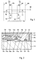
- This SRAM cell includes a transfer transistor 104 between a bit line 101 and a contact 102 for forming a conductive path so as to supply voltage from the bit line 101 to the inside of the memory cell.
- the gate of the transfer transistor 101 is connected to a word line 103.
- the contact 102 is connected to the drains of a P-type thin film transistor 105 having a source connected to a power supply line Vcc and an N-type transistor 106 having a source connected to a GND line Vss.
- the contact 102 is further connected to the gates of a P-type thin film transistor 107 the source of which is connected to Vcc of the power supply, and of a drive transistor 108 the source of which is connected to Vss of GND.
- a transfer transistor 111 is provided for forming a conductive path between a bit line 109 and a contact 110 to supply voltage from the bit line 109 to the inside of the memory cell.
- the gate of the transfer transistor 111 is connected to the word line 103.
- the contact 110 is connected to the gates of the P-type thin film transistor 107 the source of which is connected to the power supply, and of the N-type drive transistor 108 the source of which is connected to GND.
- the contact 110 is connected to the gates of the P-type thin film transistor 105 the source of which is connected to the power supply, and of the N-type drive transistor 106 the source of which is connected to GND.
- bit line 101 is at 'H' level
- bit line 109 is at 'L' level.
- the transfer transistors 104 and 111 become conductive.
- 'H' level on the bit line 101 is decreased by the threshold voltage of the transfer transistor 104, and conducted to the contact 102 through the transfer transistor 104. Since the contact 102 is connected to the gates of the P-type thin film transistor 107 and the N-type drive transistor 108, the transistor 107 is turned to OFF state and the transistor 108 is turned to ON state so that the contact 110 becomes 'L' level.
- the thin film transistor 105 to the gate of which the contact 110 is connected is turned to ON state, and the transistor 106 is turned to OFF state so that the contact 110 becomes 'L' level.
- the contact 102 continues to maintain 'H' level, the contact 110 continues to maintain 'L' level.
- bit line 101 When the bit line 101 is 'L' level, and the bit line 109 is 'H' level, similar operation continues to maintain the contact 102 at 'L' level and the contact 110 at 'H' level.
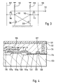
- an N-type diffusion layer 124a with low concentration is connected to the N-type diffusion layer 124'.
- the N-type diffusion layer 124a is connected to the first polycrystal silicon layer 126a doped with N-type impurities.
- the first silicide layer 127a which is mixture of silicon and metal with high melting point is provided on the first polycrystal silicon layer 126a.
- these drive transistors or transfer transistors are insulated and isolated each other by an element isolation/insulation film 128. Then, a tungsten layer 129 is formed to be the above-mentioned GND Vss wiring.
- the above-mentioned first silicide layer 127a is connected to a second polycrystal silicon layer 130 provided thereon and doped with N-type impurities.
- the second polycrystal silicon layer 130 is connected to a second silicide layer 131. These two layers are connected to the P-type thin film transistor 107 shown in FIG. 1.
- the second silicide layer 131 is connected to a third polycrystal silicon layer 132 provided thereon and doped with P-type impurities. This becomes a drain diffusion layer of the P-type thin film transistor 105 shown in FIG. 1.
- an electrode constituted by a second polycrystal silicon layer 130a and a second silicide layer 131a becomes the gate electrode of the above-mentioned thin film transistor.
- a gate insulation film 133 for the thin film transistor is formed by a silicon oxide film.
- a transfer transistor 104 is provided between a bit line 101 and a contact 102 for forming a conductive path so as to supply voltage from the bit line 101 to the inside of the memory cell.
- the gate of the transfer transistor 104 is connected to a lead wire 103.
- the contact 102 is connected to a resistor 112 one end of which is connected to Vcc of the power supply and the drain of an N-type transistor 106 the source of which is connected to GND Vss.
- the contact 102 is connected to the gate of a transfer transistor 108 the source of which is connected to GND.
- a transfer transistor 111 is connected between a bit line 109 and a contact 110 for forming a conductive path so as to supply voltage from the bit line 109 to the inside of the memory cell.
- the gate of the transfer transistor 111 is connected to the lead wire 103.
- the contact 110 is connected to a resistor 113 one end of which is connected to the power supply and the drain of an N-type transistor 108 the source of which is connected to GND.
- the contact 110 is connected to the gate of an N-type transistor 106 the source of which is connected to GND. This equivalently constitutes a flip-flop.
- bit line 101 is at 'H' level
- bit line 109 is at 'L' level.
- the word line 103 turns to 'H' level
- the transfer transistors 104 and 111 are turned to ON state.
- 'H' level on the bit line 101 is connected to the contact 102 through the transfer transistor 104.
- the contact 102 is connected to the gate of the transistor 108, the transistor 108 is turned to ON state.
- the contact 110 becomes 'L' level because the amount of current which the transistor 108 causes to flow to GND is more than the amount of current flowing through the resistor 113.
- 'L' level is provided to the gate of the drive transistor 106 connected to the contact 110 so that the drive transistor 106 is turned to OFF state. Consequently, the contact 102 becomes 'H' level. At the moment, even if the word line 103 changes to 'L' level, the contact 102 continues to maintain 'H' level, the contact 110 continuous to maintain 'L' level.
- the contact 102 maintains 'L' level, and the contact 110 maintains 'H' level.
- an aluminum wiring layer 121 and a titanium wiring layer 122 are coupled as one wiring layer to form a bit line 101 shown in FIG. 3.
- the titanium wiring layer 122 is connected to an N-type diffusion layer 124 formed on a P-type silicon substrate 123.
- MOS transistor having a source-drain region constituted by N-type diffusion layers 124 and 124', a gate electrode constituted by a gate insulation film 125, and a gate electrode constituted by a first polycrystal silicon layer 126 and a first silicide layer 127.
- the N-type diffusion layer 124' is laterally connected to an N-type diffusion layer 124a with low concentration. It is further connected to a first polycrystal silicon layer 126a doped with N-type impurities. To reduce resistance of the first polycrystal silicon layer 126 a doped with N-type impurities, it is coupled to a first silicide layer 127a. This forms the wiring shown in FIG. 3, and connected to the gate electrode of the transistor 108 and the drain of the transistor 106. Then, there is provided a tungsten layer 129 serving as a GND Vss wiring. The first silicide layer 127a is connected to a high resistance layer 135. The high resistance layer 135 is formed from polycrystal silicon containing 20 - 30% of oxygen atoms.
- the voltage at the contact 102 (or 110) is also decreased in accordance therewith through the transistor 105 (or 107) or the resistor 112 (or 113).
- the voltage at the contact 102 (or 110) is decreased up to such a level that is lower than the threshold level of the transistor 108 (or 106)
- the transistor 108 (or 106) is rendered non-conductive.
- the data stored in this memory cell is thus destroyed.
- the voltage on the power supply line Vcc decreased such a level that causes the transistor 108 (or 106) to be rendered non-conductive, the data stored in the memory cell is destroyed.
- the means that the data stored in the cell is destroyed even by a temporary change in voltage on the power supply line Vcc.
- an object of the present invention to provide a semiconductor device including an improved memory cell.
- Another object of the present invention is to provide a semiconductor device having a static memory cell provided with data retaining means for preventing data from being destroyed even under temporary lowering of a power supply voltage.
- a semiconductor device comprises a supply terminal and an memory cell which has a flip-flop circuit, said memory cell includes an diode connected in a forward direction between said supply terminal and the input terminal of said flip-flop circuit to supply current from said supply terminal to said input terminal.
- the diode performs rectifying operation to prevent the current from flowing from the input terminal to the supply terminal.
- no current path is produced from the input terminal of the flip-flop circuit to the supply terminal. Accordingly, the voltage at the input terminal does not change so that the information on the flip-flop circuit would be maintained.
- a memory cell employed in an SRAM as a first embodiment of the present invention.
- an N-type transfer transistor 4 is provided between a bit line 1 and a contact 2 for supplying voltage form the bit line 1 to the inside of the memory cell so as to form a conductive path.
- the gate of the transfer transistor 4 is connected to a word line 3.
- the drain of a P-type thin film transistor 5, the source of which is connected a supply terminal 100 is connected to the anode of a PN junction diode 6.
- the cathode of the PN junction diode 6 is connected to the contact 2.
- the contact 2 is connected to the drain of an N-type transistor 7, the source of which is connected to GND Vss, as well as to the gates of a P-type thin film transistor 8 the source of which is connected to the power supply, and of an N-type transistor the source of which is connected to GND.
- a transfer transistor 12 is provided between a bit line 10 and a node 11 for supplying voltage from the bit line 10 to the inside of the memory cell so as to form a conductive path.
- the gate of the transfer transistor 12 is connected to the word line 3.
- the drain of a P-type thin film transistor 8, the source of which is connected to a supply terminal 100 is connected to the anode of a PN junction diode 13.
- the cathode of the PN junction diode is connected to the node 11.
- the node 11 is connected to the drain of the transistor 9, as well as the gates of the thin film transistor 5 and of the transistor 7 to form a flip-flop.
- the supply terminals 100 is applied with a voltage Vcc.
- the diode 6 is connected between node 2 and the transistor 5, but it can also be used that the diode 6 is connected between the supply terminal 100 and the transistor 5. It can also be used that the diode 13 is connected between the supply terminal 100 and the transistor 8.
- bit line 1 shown in FIG. 5 is at 'H' level
- bit line 10 is at 'L' level.
- the transfer transistors 4 and 12 are turned to ON state so that 'H' level on the bit line 1 is reduced by the threshold voltage of the transfer transistor 4 through the transfer transistor 4 and supplied to the node 2. Since the node 2 is connected to the gates of the thin film transistor 8 and the transistor 9, the thin film transistor 8 is turned to OFF state, the transistor 9 is turned to ON state, and the node 11 becomes 'L' level.
- the thin film transistor 5, the gate of which the node 11 is connected, is turned to ON state.
- the transistor 7 is turned to OFF state so that current flows from the power supply to the node 2 through the thin film transistor 5 and the forward connected PN junction diode 6 so that the voltage at the node 2 is made the supply voltage Vcc.
- the nodes 2 and 11 maintain 'H' level and 'L' level, respectively.
- the node 2 can continue to maintain 'H' level. Thus, storage information is maintained.
- the node 2 continues to maintain 'L' level, the contact 11 'H' level.
- the PN junction diodes 6 and 13 are formed between the thin film transistors 5 and 8, which are the load transistors of the memory cell, and the drive transistors 7 and 9, respectively. The destruction of the storage information is prevented even if the supply Vcc is instantaneously broken.
- FIG. 6 is a sectional view of TFT type memory cell according to the present invention.
- Two layers of an aluminum wiring layer 21 and a titanium wiring layer 22 are coupled to form a bit line 1 shown in FIG. 1.
- the titanium wiring layer 22 is connected to an N-type diffusion layer 24 formed on a P-type silicon substrate 23.
- N-type diffusion layer 24 formed on a P-type silicon substrate 23.
- MOS transistor having N-type diffusion layers 24 and 24' as its source-drain, a gate insulation film 25 as its gate electrode, and a first polycrystal silicon layer 26 and a first silicide layer 27 as its gate electrode.
- the N-type diffusion layer 24' is laterally connected to an N-type diffusion layer 24a with low concentration.
- first polycrystal silicon layer 26a doped with N-type impurities.
- first silicide layer 27a there is a first silicide layer 27a thereon, and these two layers are coupled. These two layers are connected to the gate electrode of the transistor 9 and the drain of the transistor 7. These transistors are insulated and isolated by an element isolation/insulation film 28. Furthermore, a tungsten layer 29 is formed serving as wiring for GND Vss.
- the first silicide layer 27a is connected to a second polycrystal silicon layer 30 doped with N-type impurities.
- the second polycrystal silicon layer 30 connects to the gate electrode of the thin film transistor 8.
- the second polycrystal silicon layer 30 directly connects to a P-type silicon layer 31 doped with P-type impurities thus a PN junction diode is formed.
- the P-type silicon layer 31 is connected to a third polycrystal silicon layer 32.
- the second polycrystal silicon layer 30a becomes the gate electrode of the thin film transistor 5, and an insulation layer 33 becomes the gate insulation film of the thin film transistor 5.
- the third polycrystal silicon layer 32 is doped with N-type impurities for the source-drain region and P-type impurities for the channel region.
- the TFT type memory cell of the present invention is produced.
- FIG. 7 is the circuit diagram of a resistance memory cell.
- a transfer transistor 4 is provided between a bit line 1 and a node 2 for supplying voltage from the bit line 1 to the inside of the memory cell so as to form a conductive path.
- the gate of the transfer transistor 4 is connected to a word line 3.
- One end of a resistor 14, the other end of which is connected to a supply terminal 100, is connected to the anode of a PN junction diode 6.
- the cathode of the PN junction diode 6 is connected to the node 2.
- the node 2 is connected to the gate of an N-type transistor 9 the source of which is connected to GND, and the drain of an N-type transistor 7 the source of which is connected to GND.
- a transfer transistor 12 is connected between a bit line 10 and a node 11 for supplying voltage from the bit line 10 to the inside of the memory cell so as to form a conductive path.
- the gate of the transfer transistor 12 is connected to the word line 3.
- An resistor 15 one end of which is connected to a supply terminal 100 is connected to the anode of a PN junction diode 13 with the other end.
- the cathode of the PN junction diode 13 is connected to the node 11.
- the node 11 is connected to the gate of the transistor 7 and the drain of the transistor 9 to equivalently form a flip-flop.
- the supply terminal 100 is applied with the voltage Vcc.
- the diode 6 is connected between node 2 and a resistor 14, but it can also be used that the diode 6 is connected between the supply terminal 100 and the resistor 14. It can also be used that diode 13 is connected between the supply terminal 100 and the resistor 15.
- bit line 1 is at 'H' level
- bit line 10 is at 'L' level.
- the word line 3 becomes 'H' level
- the drive transistors 4 and 12 are turned to ON state, and 'H' level on the bit line 1 is transferred to the node 2 through the transistor 4. Since the node 2 is connected to the gate of the transistor 9, the transistor 9 is turned to ON state. At the moment, the node 11 becomes 'L' level. 'L' level is provided to the gate of the transistor 7 which is turned to OFF state, and the node 2 becomes 'H' level.
- the node 2 continues to maintain 'H' level, the contact 11 'L' level.
- the node 2 continues to maintain 'H' level, the contact 11 'L' level.
- the node 2 continues to maintain 'L' level, the node 11 'H' level.
- FIG. 8 shows a sectional view of the resistance memory cell according to the present invention.
- two layers of an aluminum wiring layer 21 and a titanium wiring layer 22 are coupled as a bit line 1 shown in FIG. 7.
- a MOS transistor having N-type diffusion layers 24 and 24' as its source-drain, and a gate electrode constituted by a gate insulation film 25, a first polycrystal silicon layer 26, and a first silicide layer 27.
- This transistor corresponds to the transfer transistor 4 in FIG. 7.
- the electrode constituted by a first polycrystal silicon layer 26a and a first silicide layer 27a which connects to an N-type diffusion layer 24a serves as the gate electrode of the transistor 9 shown in FIG. 7.
- a tungsten layer 29 is formed. This layer is secured to the ground potential shown in FIG. 7.
- an N-type silicon layer 35 and a P-type silicon layer 36 are formed.
- a PN junction diode is formed at the junction of the N-type silicon layer 35 and the P-type silicon layer 36.
- the N-type silicon layer 35 and the P-type silicon layer consist of a monocrystal or polycrystal silicon film the impurity concentration of which is determined in a similar manner to the first embodiment.
- a high resistance layer 37 is formed connecting the P-type silicon layer 36.
- the high resistance layer 37 consists of polycrystal silicon containing 20 - 30% oxygen atoms. This corresponds to the high resistance element 14 shown in FIG. 7.
- a PN junction diode is connected in series between a contact at the drain of a P-type thin film transistor the contact at the source of which is connected to the power supply, and a contact at the drain of a drive transistor a contact at the source of which is connected to GND.
- a PN junction diode is connected in series between an end of a resistance the other end of which is connected to the power supply, and a contact of the drain of a transistor a contact at the source of which is connected to GND.
- a PN junction diode is connected in series between a supply line in a semiconductor chip, and a supply line which supplies the supply voltage to a memory cell group.
- the present invention is very robust against variation of the supply voltage. For example, it can secure a longer data holding time by about 100-fold than that in the prior art.
- the present invention can hold data for about ten seconds even if the supply is exhausted so that there is provided an advantage that a time for replacing the cell or battery can be obtained.
- the size of memory cell in an SRAM is not increased over the conventional memory cell. That is, the structure according to the present invention is suitable for higher integration or density so that improvement of capacity and quality of SRAM can be attained.
Landscapes
- Engineering & Computer Science (AREA)
- Microelectronics & Electronic Packaging (AREA)
- Computer Hardware Design (AREA)
- Semiconductor Memories (AREA)
- Thin Film Transistor (AREA)
- Metal-Oxide And Bipolar Metal-Oxide Semiconductor Integrated Circuits (AREA)
- Static Random-Access Memory (AREA)
Abstract
A semiconductor device has a memory cell which is constituted of a flip-flop circuit operating on power voltage between power supply lines 100 and 101. This memory cell further includes diodes 6 and 13, each of which is connected in series with a load of the flip-flop circuit between the power supply terminal 100 and each of input/output nodes of said flip-flop circuit.
Description
- The present invention relates to a semiconductor device and, more particularly, to such a device that has a static memory cell for temporarily storing data.
- A static memory cell is employes as a data holding element for a static random memory device (SRAM), a data register of a microcontroller and so on. Such a memory cell is generally constructed with a flip-flop in which two inverters are connected such that input and output nodes of one inverter are connected respectively to output and input nodes of the other inverter. Each of the inverters includes a insulated gate transistor such as a MOS transistor having a gate electrode connected to the input node and a drain-source current path connected between the output node and a first power supply line and a load element connected between the output node and a second power supply line. The load element is constituted of a resistor or an insulated gate transistor such as a MOS transistor as a thin film transistor (TFT).
- Referring now to Figs. 1 and 2, there is shown one memory cell employed in an SRAM. This SRAM cell includes a
transfer transistor 104 between abit line 101 and acontact 102 for forming a conductive path so as to supply voltage from thebit line 101 to the inside of the memory cell. The gate of thetransfer transistor 101 is connected to aword line 103. Thecontact 102 is connected to the drains of a P-typethin film transistor 105 having a source connected to a power supply line Vcc and an N-type transistor 106 having a source connected to a GND line Vss. Thecontact 102 is further connected to the gates of a P-typethin film transistor 107 the source of which is connected to Vcc of the power supply, and of adrive transistor 108 the source of which is connected to Vss of GND. Moreover, atransfer transistor 111 is provided for forming a conductive path between abit line 109 and acontact 110 to supply voltage from thebit line 109 to the inside of the memory cell. The gate of thetransfer transistor 111 is connected to theword line 103. Thecontact 110 is connected to the gates of the P-typethin film transistor 107 the source of which is connected to the power supply, and of the N-type drive transistor 108 the source of which is connected to GND. In addition, thecontact 110 is connected to the gates of the P-typethin film transistor 105 the source of which is connected to the power supply, and of the N-type drive transistor 106 the source of which is connected to GND. Thus, a flip-flop is constituted. - Now, the storing operation of the TFT type memory cell will be explained.
- First, a case is assumed where the
bit line 101 is at 'H' level, and thebit line 109 is at 'L' level. When theword line 103 turns to 'H' level, thetransfer transistors bit line 101 is decreased by the threshold voltage of thetransfer transistor 104, and conducted to thecontact 102 through thetransfer transistor 104. Since thecontact 102 is connected to the gates of the P-typethin film transistor 107 and the N-type drive transistor 108, thetransistor 107 is turned to OFF state and thetransistor 108 is turned to ON state so that thecontact 110 becomes 'L' level. Thethin film transistor 105 to the gate of which thecontact 110 is connected is turned to ON state, and thetransistor 106 is turned to OFF state so that thecontact 110 becomes 'L' level. At the moment, even if the word line changes to 'L' level, thecontact 102 continues to maintain 'H' level, thecontact 110 continues to maintain 'L' level. - When the
bit line 101 is 'L' level, and thebit line 109 is 'H' level, similar operation continues to maintain thecontact 102 at 'L' level and thecontact 110 at 'H' level. - In a device structure of this memory cell as shown in Fig. 2, an aluminum
wi ring layer 121 and atitanium wiring layer 122 are coupled as one wiring layer to form abit line 101 shown in FIG. 1. Moreover, thetitanium wiring layer 122 is connected to an N-type diffusion layer 124 formed on asilicon substrate 123 with conductivity type of P. Here, as shown in FIG. 2, there is formed a MOS transistor having a source-drain region constituted by N-type diffusion layers 124 and 124', a gate electrode constituted by agate insulation film 125, and a gate electrode constituted by a firstpolycrystal silicon layer 126 and afirst silicide layer 127. This MOS transistor is atransfer transistor 104 shown in FIG. 1. - Then, an N-
type diffusion layer 124a with low concentration is connected to the N-type diffusion layer 124'. In addition, the N-type diffusion layer 124a is connected to the firstpolycrystal silicon layer 126a doped with N-type impurities. To reduce resistance of the firstpolycrystal silicon layer 126a, thefirst silicide layer 127a which is mixture of silicon and metal with high melting point is provided on the firstpolycrystal silicon layer 126a. These two layers constitutes the gate electrode of thetransistor 108 of FIG. 1. - Here, these drive transistors or transfer transistors are insulated and isolated each other by an element isolation/
insulation film 128. Then, atungsten layer 129 is formed to be the above-mentioned GND Vss wiring. - The above-mentioned
first silicide layer 127a is connected to a secondpolycrystal silicon layer 130 provided thereon and doped with N-type impurities. In addition, the secondpolycrystal silicon layer 130 is connected to asecond silicide layer 131. These two layers are connected to the P-typethin film transistor 107 shown in FIG. 1. Moreover, thesecond silicide layer 131 is connected to a thirdpolycrystal silicon layer 132 provided thereon and doped with P-type impurities. This becomes a drain diffusion layer of the P-typethin film transistor 105 shown in FIG. 1. Here, an electrode constituted by a secondpolycrystal silicon layer 130a and asecond silicide layer 131a becomes the gate electrode of the above-mentioned thin film transistor. Also, agate insulation film 133 for the thin film transistor is formed by a silicon oxide film. - Turning to Figs. 3 and 4, there is shown another memory cell employed in an SRAM. In this cell, a
transfer transistor 104 is provided between abit line 101 and acontact 102 for forming a conductive path so as to supply voltage from thebit line 101 to the inside of the memory cell. The gate of thetransfer transistor 104 is connected to alead wire 103. Thecontact 102 is connected to aresistor 112 one end of which is connected to Vcc of the power supply and the drain of an N-type transistor 106 the source of which is connected to GND Vss. In addition, thecontact 102 is connected to the gate of atransfer transistor 108 the source of which is connected to GND. Furthermore, atransfer transistor 111 is connected between abit line 109 and acontact 110 for forming a conductive path so as to supply voltage from thebit line 109 to the inside of the memory cell. The gate of thetransfer transistor 111 is connected to thelead wire 103. Thecontact 110 is connected to aresistor 113 one end of which is connected to the power supply and the drain of an N-type transistor 108 the source of which is connected to GND. Thecontact 110 is connected to the gate of an N-type transistor 106 the source of which is connected to GND. This equivalently constitutes a flip-flop. - Now, the storing operation of the resistance memory cell will be explained. A case is assumed where the
bit line 101 is at 'H' level, and thebit line 109 is at 'L' level. When theword line 103 turns to 'H' level, thetransfer transistors bit line 101 is connected to thecontact 102 through thetransfer transistor 104. Since thecontact 102 is connected to the gate of thetransistor 108, thetransistor 108 is turned to ON state. Thecontact 110 becomes 'L' level because the amount of current which thetransistor 108 causes to flow to GND is more than the amount of current flowing through theresistor 113. 'L' level is provided to the gate of thedrive transistor 106 connected to thecontact 110 so that thedrive transistor 106 is turned to OFF state. Consequently, thecontact 102 becomes 'H' level. At the moment, even if theword line 103 changes to 'L' level, thecontact 102 continues to maintain 'H' level, thecontact 110 continuous to maintain 'L' level. - In a case where the
bit line 101 is at 'L' level, and thebit line 109 is at 'H' level, under a similar operation, thecontact 102 maintains 'L' level, and thecontact 110 maintains 'H' level. - In a device structure of the memory cell of Fig. 3, as shown in FIG. 4, an
aluminum wiring layer 121 and atitanium wiring layer 122 are coupled as one wiring layer to form abit line 101 shown in FIG. 3. Moreover, thetitanium wiring layer 122 is connected to an N-type diffusion layer 124 formed on a P-type silicon substrate 123. Here, as described earlier, there is formed a MOS transistor having a source-drain region constituted by N-type diffusion layers 124 and 124', a gate electrode constituted by agate insulation film 125, and a gate electrode constituted by a firstpolycrystal silicon layer 126 and afirst silicide layer 127. Then, the N-type diffusion layer 124' is laterally connected to an N-type diffusion layer 124a with low concentration. It is further connected to a firstpolycrystal silicon layer 126a doped with N-type impurities. To reduce resistance of the firstpolycrystal silicon layer 126 a doped with N-type impurities, it is coupled to afirst silicide layer 127a. This forms the wiring shown in FIG. 3, and connected to the gate electrode of thetransistor 108 and the drain of thetransistor 106. Then, there is provided atungsten layer 129 serving as a GND Vss wiring. Thefirst silicide layer 127a is connected to ahigh resistance layer 135. Thehigh resistance layer 135 is formed from polycrystal silicon containing 20 - 30% of oxygen atoms. - In the memory cell as described above, when the voltage on the power supply line Vcc decreases, the voltage at the contact 102 (or 110) is also decreased in accordance therewith through the transistor 105 (or 107) or the resistor 112 (or 113). When the voltage at the contact 102 (or 110) is decreased up to such a level that is lower than the threshold level of the transistor 108 (or 106), the transistor 108 (or 106) is rendered non-conductive. The data stored in this memory cell is thus destroyed. In other words, the voltage on the power supply line Vcc decreased such a level that causes the transistor 108 (or 106) to be rendered non-conductive, the data stored in the memory cell is destroyed. The means that the data stored in the cell is destroyed even by a temporary change in voltage on the power supply line Vcc.
- It is, therefore, an object of the present invention to provide a semiconductor device including an improved memory cell.
- Another object of the present invention is to provide a semiconductor device having a static memory cell provided with data retaining means for preventing data from being destroyed even under temporary lowering of a power supply voltage.
- A semiconductor device according to the present invention comprises a supply terminal and an memory cell which has a flip-flop circuit, said memory cell includes an diode connected in a forward direction between said supply terminal and the input terminal of said flip-flop circuit to supply current from said supply terminal to said input terminal.
- According to this arrangement, even if potential on the supply terminal is instantaneously broken, the diode performs rectifying operation to prevent the current from flowing from the input terminal to the supply terminal. Thus, no current path is produced from the input terminal of the flip-flop circuit to the supply terminal. Accordingly, the voltage at the input terminal does not change so that the information on the flip-flop circuit would be maintained.
- The above and other objects, features and advantages of the present invention will be more apparent from the following description taken in conjunction with the accompanying drawings, in which:
- FIG. 1 is a circuit diagram of a conventional TFT type memory cell;
- FIG. 2 is the structure of the conventional TFT type memory cell;
- FIG. 3 is a circuit diagram of a conventional high resistance memory cell;
- FIG. 4 is the structure of the conventional high resistance memory cell;
- FIG. 5 is a circuit diagram illustrating a first embodiment of the present invention;
- FIG. 6 is the structure illustrating the first embodiment of the present invention;
- FIG. 7 is a circuit diagram illustrating a second embodiment of the present invention; and
- FIG. 8 is the structure illustrating the second embodiment of the present invention.
- Referring now to Fig. 5, there is shown a memory cell employed in an SRAM as a first embodiment of the present invention. In this memory cell, an N-type transfer transistor 4 is provided between a bit line 1 and a
contact 2 for supplying voltage form the bit line 1 to the inside of the memory cell so as to form a conductive path. The gate of the transfer transistor 4 is connected to aword line 3. Moreover, the drain of a P-type thin film transistor 5, the source of which is connected asupply terminal 100, is connected to the anode of a PN junction diode 6. The cathode of the PN junction diode 6 is connected to thecontact 2. In addition, thecontact 2 is connected to the drain of an N-type transistor 7, the source of which is connected to GND Vss, as well as to the gates of a P-typethin film transistor 8 the source of which is connected to the power supply, and of an N-type transistor the source of which is connected to GND. Atransfer transistor 12 is provided between abit line 10 and anode 11 for supplying voltage from thebit line 10 to the inside of the memory cell so as to form a conductive path. The gate of thetransfer transistor 12 is connected to theword line 3. In addition, the drain of a P-typethin film transistor 8, the source of which is connected to asupply terminal 100, is connected to the anode of aPN junction diode 13. The cathode of the PN junction diode is connected to thenode 11. In addition, thenode 11 is connected to the drain of thetransistor 9, as well as the gates of the thin film transistor 5 and of thetransistor 7 to form a flip-flop. - The
supply terminals 100 is applied with a voltage Vcc. - In FIG. 5, the diode 6 is connected between
node 2 and the transistor 5, but it can also be used that the diode 6 is connected between thesupply terminal 100 and the transistor 5. It can also be used that thediode 13 is connected between thesupply terminal 100 and thetransistor 8. - Now, the storing operation of the present invention will be explained. A case is assumed where the bit line 1 shown in FIG. 5 is at 'H' level, and a
bit line 10 is at 'L' level. When theword line 3 becomes 'H' level, thetransfer transistors 4 and 12 are turned to ON state so that 'H' level on the bit line 1 is reduced by the threshold voltage of the transfer transistor 4 through the transfer transistor 4 and supplied to thenode 2. Since thenode 2 is connected to the gates of thethin film transistor 8 and thetransistor 9, thethin film transistor 8 is turned to OFF state, thetransistor 9 is turned to ON state, and thenode 11 becomes 'L' level. The thin film transistor 5, the gate of which thenode 11 is connected, is turned to ON state. Thetransistor 7 is turned to OFF state so that current flows from the power supply to thenode 2 through the thin film transistor 5 and the forward connected PN junction diode 6 so that the voltage at thenode 2 is made the supply voltage Vcc. At the moment, even if theword line 3 changes to 'L' level, thenodes node 2 can continue to maintain 'H' level. Thus, storage information is maintained. - In a case where the bit line 1 is at 'L' level, and the
bit line 10 is at 'H' level, in a similar operation, thenode 2 continues to maintain 'L' level, the contact 11 'H' level. - That is, since the
PN junction diodes 6 and 13 are formed between thethin film transistors 5 and 8, which are the load transistors of the memory cell, and thedrive transistors - Then, the device structure of the present invention is described with reference to FIG. 6. FIG. 6 is a sectional view of TFT type memory cell according to the present invention. Two layers of an
aluminum wiring layer 21 and atitanium wiring layer 22 are coupled to form a bit line 1 shown in FIG. 1. Moreover, thetitanium wiring layer 22 is connected to an N-type diffusion layer 24 formed on a P-type silicon substrate 23. Here, there is formed a MOS transistor having N-type diffusion layers 24 and 24' as its source-drain, agate insulation film 25 as its gate electrode, and a firstpolycrystal silicon layer 26 and afirst silicide layer 27 as its gate electrode. Then, the N-type diffusion layer 24' is laterally connected to an N-type diffusion layer 24a with low concentration. In addition, it is connected to a firstpolycrystal silicon layer 26a doped with N-type impurities. To reduce the resistance of the firstpolycrystal silicon layer 26a doped with N-type impurities, there is afirst silicide layer 27a thereon, and these two layers are coupled. These two layers are connected to the gate electrode of thetransistor 9 and the drain of thetransistor 7. These transistors are insulated and isolated by an element isolation/insulation film 28. Furthermore, atungsten layer 29 is formed serving as wiring for GND Vss. - The
first silicide layer 27a is connected to a secondpolycrystal silicon layer 30 doped with N-type impurities. The secondpolycrystal silicon layer 30 connects to the gate electrode of thethin film transistor 8. In addition, the secondpolycrystal silicon layer 30 directly connects to a P-type silicon layer 31 doped with P-type impurities thus a PN junction diode is formed. The P-type silicon layer 31 is connected to a thirdpolycrystal silicon layer 32. The secondpolycrystal silicon layer 30a becomes the gate electrode of the thin film transistor 5, and aninsulation layer 33 becomes the gate insulation film of the thin film transistor 5. The thirdpolycrystal silicon layer 32 is doped with N-type impurities for the source-drain region and P-type impurities for the channel region. - Then, the TFT type memory cell of the present invention is produced.
- Next, as a second embodiment, a resistance memory cell will be explained based on FIGS. 7 and 8.
- FIG. 7 is the circuit diagram of a resistance memory cell. A transfer transistor 4 is provided between a bit line 1 and a
node 2 for supplying voltage from the bit line 1 to the inside of the memory cell so as to form a conductive path. The gate of the transfer transistor 4 is connected to aword line 3. One end of a resistor 14, the other end of which is connected to asupply terminal 100, is connected to the anode of a PN junction diode 6. The cathode of the PN junction diode 6 is connected to thenode 2. In addition, thenode 2 is connected to the gate of an N-type transistor 9 the source of which is connected to GND, and the drain of an N-type transistor 7 the source of which is connected to GND. In addition, atransfer transistor 12 is connected between abit line 10 and anode 11 for supplying voltage from thebit line 10 to the inside of the memory cell so as to form a conductive path. The gate of thetransfer transistor 12 is connected to theword line 3. An resistor 15 one end of which is connected to asupply terminal 100 is connected to the anode of aPN junction diode 13 with the other end. The cathode of thePN junction diode 13 is connected to thenode 11. In addition, thenode 11 is connected to the gate of thetransistor 7 and the drain of thetransistor 9 to equivalently form a flip-flop. - The
supply terminal 100 is applied with the voltage Vcc. - In FIG. 7, the diode 6 is connected between
node 2 and a resistor 14, but it can also be used that the diode 6 is connected between thesupply terminal 100 and the resistor 14. It can also be used thatdiode 13 is connected between thesupply terminal 100 and the resistor 15. - Now, the storing operation of the resistance memory cell according to the present invention will be explained by using FIG. 7. It is assumed that the bit line 1 is at 'H' level, and the
bit line 10 is at 'L' level. When theword line 3 becomes 'H' level, thedrive transistors 4 and 12 are turned to ON state, and 'H' level on the bit line 1 is transferred to thenode 2 through the transistor 4. Since thenode 2 is connected to the gate of thetransistor 9, thetransistor 9 is turned to ON state. At the moment, thenode 11 becomes 'L' level. 'L' level is provided to the gate of thetransistor 7 which is turned to OFF state, and thenode 2 becomes 'H' level. At the moment, even if theword line 3 changes to 'L' level, thenode 2 continues to maintain 'H' level, the contact 11 'L' level. In addition, similar to the first embodiment, even if the supply voltage Vcc varies, thenode 2 continues to maintain 'H' level, the contact 11 'L' level. - When the bit line 1 is at 'L' level, and the
bit line 10 is at 'H' level, in a similar operation, thenode 2 continues to maintain 'L' level, the node 11 'H' level. - Then, the device structure of the resistance memory cell according to the present invention is described based on FIG. 8. FIG. 8 shows a sectional view of the resistance memory cell according to the present invention.
- Similar to the first embodiment, two layers of an
aluminum wiring layer 21 and atitanium wiring layer 22 are coupled as a bit line 1 shown in FIG. 7. Then, similar to the first embodiment, there is formed a MOS transistor having N-type diffusion layers 24 and 24' as its source-drain, and a gate electrode constituted by agate insulation film 25, a firstpolycrystal silicon layer 26, and afirst silicide layer 27. This transistor corresponds to the transfer transistor 4 in FIG. 7. In addition, the electrode constituted by a firstpolycrystal silicon layer 26a and afirst silicide layer 27a which connects to an N-type diffusion layer 24a serves as the gate electrode of thetransistor 9 shown in FIG. 7. Then, atungsten layer 29 is formed. This layer is secured to the ground potential shown in FIG. 7. - After such arrangement is formed, an N-
type silicon layer 35 and a P-type silicon layer 36 are formed. Then, a PN junction diode is formed at the junction of the N-type silicon layer 35 and the P-type silicon layer 36. This corresponds to the PN junction diode 6 shown in FIG. 7. Here, the N-type silicon layer 35 and the P-type silicon layer consist of a monocrystal or polycrystal silicon film the impurity concentration of which is determined in a similar manner to the first embodiment. Furthermore, ahigh resistance layer 37 is formed connecting the P-type silicon layer 36. Thehigh resistance layer 37 consists of polycrystal silicon containing 20 - 30% oxygen atoms. This corresponds to the high resistance element 14 shown in FIG. 7. - As described in the above, according to the present invention, in an SRAM memory cell, a PN junction diode is connected in series between a contact at the drain of a P-type thin film transistor the contact at the source of which is connected to the power supply, and a contact at the drain of a drive transistor a contact at the source of which is connected to GND. Alternatively, a PN junction diode is connected in series between an end of a resistance the other end of which is connected to the power supply, and a contact of the drain of a transistor a contact at the source of which is connected to GND. Furthermore, a PN junction diode is connected in series between a supply line in a semiconductor chip, and a supply line which supplies the supply voltage to a memory cell group.
- With such arrangements, data is prevented from being destroyed when the supply voltage drops or is instantaneously broken during operation of the SRAM. In addition, the present invention is very robust against variation of the supply voltage. For example, it can secure a longer data holding time by about 100-fold than that in the prior art. Thus, when it is used in a product the power supply of which relies on a dry cell or battery, while data in the memory cell will be destroyed in the prior art when the dry cell or battery is exchanged, the present invention can hold data for about ten seconds even if the supply is exhausted so that there is provided an advantage that a time for replacing the cell or battery can be obtained.
- Furthermore, according to the present invention, the size of memory cell in an SRAM is not increased over the conventional memory cell. That is, the structure according to the present invention is suitable for higher integration or density so that improvement of capacity and quality of SRAM can be attained.
- It is apparent that the present invention is not limited to the above embodiments but may be modified and changed without departing from the scope and spirit of the invention.
Claims (7)
- A semiconductor device having at least one memory cell, said memory cell comprising a first inverter operating on a voltage between first and second power supply lines and having a first input node and a first output node, a second inverter operating on said voltage and a second input node coupled to said first output and a second output node coupled to said first input node, and means for suppressing lowering in voltage at each of said first and second output nodes against lowering of said voltage between said first and second power supply lines.
- The device as claimed in claim 1, wherein each of said first and second inverters includes a load element coupled between an associated one of said first and second output nodes and said first power supply line and said means comprises a diode connected in series with said load element between said associated one of said first and second output nodes and said first power supply line.
- The device as claimed in claim 2, wherein said diodes is constituted of a first poly-silicon layer of a first conductivity type and a second poly-silicon layer of a second conductivity type.
- A semiconductor device comprising a first inverter, a second inverted coupled to said first inverter to form a flip-flop circuit, each of said first and second inverters including a switching transistor and a load element connected in series between first and second power supply lines, and first and second unidirectional elements each coupled in series to said load element of an associated one of said first and second inverters between said switching transistor of said associated one of said first and second inverters and said first power supply line.
- The device as claimed in claim 4, wherein each of said first and second unidirectional elements in a diode.
- The device as claimed in claim 5, wherein said diode has an anode connected to said load element and a cathode connected to said switching transistor.
- A semiconductor device comprising a supply terminal and an memory cell which has a flip-flop circuit, said memory cell including an diode connected in a forward direction between said supply terminal and the input terminal of said flip-flop circuit to supply current from said supply terminal to said input terminal.
Applications Claiming Priority (2)
| Application Number | Priority Date | Filing Date | Title |
|---|---|---|---|
| JP7103733A JP2693926B2 (en) | 1995-04-27 | 1995-04-27 | Static RAM cell |
| JP103733/95 | 1995-04-27 |
Publications (1)
| Publication Number | Publication Date |
|---|---|
| EP0740345A2 true EP0740345A2 (en) | 1996-10-30 |
Family
ID=14361844
Family Applications (1)
| Application Number | Title | Priority Date | Filing Date |
|---|---|---|---|
| EP96106786A Withdrawn EP0740345A2 (en) | 1995-04-27 | 1996-04-29 | Semiconductor device having static memory cell provided with data retaining means |
Country Status (4)
| Country | Link |
|---|---|
| EP (1) | EP0740345A2 (en) |
| JP (1) | JP2693926B2 (en) |
| KR (1) | KR960039395A (en) |
| TW (1) | TW293912B (en) |
Cited By (1)
| Publication number | Priority date | Publication date | Assignee | Title |
|---|---|---|---|---|
| EP0802564A2 (en) * | 1996-04-19 | 1997-10-22 | Nec Corporation | Semiconductor device having high resistive element including high melting point metal |
Family Cites Families (2)
| Publication number | Priority date | Publication date | Assignee | Title |
|---|---|---|---|---|
| US5135888A (en) * | 1989-01-18 | 1992-08-04 | Sgs-Thomson Microelectronics, Inc. | Field effect device with polycrystalline silicon channel |
| JPH04319598A (en) * | 1991-04-19 | 1992-11-10 | Fujitsu Ltd | Semiconductor memory |
-
1995
- 1995-04-27 JP JP7103733A patent/JP2693926B2/en not_active Expired - Lifetime
-
1996
- 1996-04-27 TW TW085105061A patent/TW293912B/zh active
- 1996-04-27 KR KR1019960013254A patent/KR960039395A/en not_active Application Discontinuation
- 1996-04-29 EP EP96106786A patent/EP0740345A2/en not_active Withdrawn
Cited By (2)
| Publication number | Priority date | Publication date | Assignee | Title |
|---|---|---|---|---|
| EP0802564A2 (en) * | 1996-04-19 | 1997-10-22 | Nec Corporation | Semiconductor device having high resistive element including high melting point metal |
| EP0802564A3 (en) * | 1996-04-19 | 1999-02-24 | Nec Corporation | Semiconductor device having high resistive element including high melting point metal |
Also Published As
| Publication number | Publication date |
|---|---|
| TW293912B (en) | 1996-12-21 |
| JPH08298293A (en) | 1996-11-12 |
| KR960039395A (en) | 1996-11-25 |
| JP2693926B2 (en) | 1997-12-24 |
Similar Documents
| Publication | Publication Date | Title |
|---|---|---|
| US6104631A (en) | Static memory cell with load circuit using a tunnel diode | |
| US6573549B1 (en) | Dynamic threshold voltage 6T SRAM cell | |
| US4639758A (en) | Metal oxide semiconductor field-effect transistor with metal source making ohmic contact to channel-base region | |
| JP2710113B2 (en) | Integrated circuits using complementary circuit technology | |
| US6849958B2 (en) | Semiconductor latches and SRAM devices | |
| US5990521A (en) | Semiconductor device and method of producing the same | |
| US4907059A (en) | Semiconductor bipolar-CMOS inverter | |
| US4516223A (en) | High density bipolar ROM having a lateral PN diode as a matrix element and method of fabrication | |
| US6674105B2 (en) | Semiconductor memory device and method of forming the same | |
| EP0054471A2 (en) | Semiconductor resistor element | |
| US5404326A (en) | Static random access memory cell structure having a thin film transistor load | |
| US4661831A (en) | Integrated RS flip-flop circuit | |
| EP0740345A2 (en) | Semiconductor device having static memory cell provided with data retaining means | |
| JPH0738434B2 (en) | Integrated circuits with complementary circuit technology | |
| US6576962B2 (en) | CMOS SRAM cell with prescribed power-on data state | |
| US4170017A (en) | Highly integrated semiconductor structure providing a diode-resistor circuit configuration | |
| JP2692439B2 (en) | Integrated circuit binary memory cell | |
| US5343087A (en) | Semiconductor device having a substrate bias generator | |
| JPH0430391A (en) | Static type semiconductor memory | |
| JP2594931B2 (en) | Semiconductor storage device | |
| KR910001423B1 (en) | Semiconductor memory device | |
| KR20010062608A (en) | Dynamic threshold voltage 6t sram cell | |
| KR20010062611A (en) | Dynamic threshold voltage 4t sram cell | |
| JP2564773B2 (en) | Method for manufacturing semiconductor integrated circuit device | |
| KR0161418B1 (en) | Pmos transistor of sram |
Legal Events
| Date | Code | Title | Description |
|---|---|---|---|
| PUAI | Public reference made under article 153(3) epc to a published international application that has entered the european phase |
Free format text: ORIGINAL CODE: 0009012 |
|
| AK | Designated contracting states |
Kind code of ref document: A2 Designated state(s): DE FR GB |
|
| STAA | Information on the status of an ep patent application or granted ep patent |
Free format text: STATUS: THE APPLICATION HAS BEEN WITHDRAWN |
|
| 18W | Application withdrawn |
Withdrawal date: 19980116 |