EP0735604A1 - Planar dielectric line and integrated circuit using the same - Google Patents
Planar dielectric line and integrated circuit using the same Download PDFInfo
- Publication number
- EP0735604A1 EP0735604A1 EP96104889A EP96104889A EP0735604A1 EP 0735604 A1 EP0735604 A1 EP 0735604A1 EP 96104889 A EP96104889 A EP 96104889A EP 96104889 A EP96104889 A EP 96104889A EP 0735604 A1 EP0735604 A1 EP 0735604A1
- Authority
- EP
- European Patent Office
- Prior art keywords
- dielectric
- substrate
- slot
- dielectric substrate
- frequency
- Prior art date
- Legal status (The legal status is an assumption and is not a legal conclusion. Google has not performed a legal analysis and makes no representation as to the accuracy of the status listed.)
- Granted
Links
Images


Classifications
-
- H—ELECTRICITY
- H01—ELECTRIC ELEMENTS
- H01P—WAVEGUIDES; RESONATORS, LINES, OR OTHER DEVICES OF THE WAVEGUIDE TYPE
- H01P3/00—Waveguides; Transmission lines of the waveguide type
- H01P3/02—Waveguides; Transmission lines of the waveguide type with two longitudinal conductors
-
- H—ELECTRICITY
- H01—ELECTRIC ELEMENTS
- H01P—WAVEGUIDES; RESONATORS, LINES, OR OTHER DEVICES OF THE WAVEGUIDE TYPE
- H01P3/00—Waveguides; Transmission lines of the waveguide type
-
- H—ELECTRICITY
- H05—ELECTRIC TECHNIQUES NOT OTHERWISE PROVIDED FOR
- H05K—PRINTED CIRCUITS; CASINGS OR CONSTRUCTIONAL DETAILS OF ELECTRIC APPARATUS; MANUFACTURE OF ASSEMBLAGES OF ELECTRICAL COMPONENTS
- H05K1/00—Printed circuits
- H05K1/02—Details
- H05K1/0213—Electrical arrangements not otherwise provided for
- H05K1/0237—High frequency adaptations
Definitions
- transmission lines have been largely used in the range of microwave and millimeter-waves, such as waveguides, coaxial lines, microstrip lines, coplanar lines, slotted lines, and so on. These transmission lines are constructed by forming predetermined electrodes on a dielectric substrate. Waveguides are for use in applications where conductor losses should be inhibited to a low level.
- Coaxial lines are widely used as connecting cables between equipment.
- Coplanar lines, microstrip lines, slotted lines, etc. are largely employed for forming connections between electronic parts, such as ICs, since they are easily connected thereto.
- the dielectric constant ⁇ r 23 and the thickness t23 of the dielectric substrate 23 and the dielectric constant ⁇ r 26 and ⁇ r 27 of the substrates 26 and 27, respectively, are set so that a planar wave having a propagation frequency fb is totally reflected on the top surface of the dielectric substrate 23 in the slot 24 and on the bottom surface of the substrate 23 close to the slot 25.
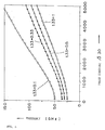
- Fig. 10 is a diagram indicating the relation between the frequency and the phase constant ⁇ 20 of the dielectric line LN20 when the widths W of the slots 24 and 25 of the substrate 23 were set at the values 0.5 mm, 1 mm, 2 mm and 3 mm.
- the values shown in Fig. 10 were calculated according to the finite-element method.
- the parameters of the structure of the dielectric line LN20 were set as follows:
Landscapes
- Waveguides (AREA)
- Control Of Motors That Do Not Use Commutators (AREA)
- Semiconductor Integrated Circuits (AREA)
Abstract
Description
- The present invention relates to a planar dielectric line for use in a microwave or millimeter-wave band. The invention also relates to an integrated circuit using the dielectric line.
- Microwaves and millimeter-waves, which are electromagnetic waves in a very wide range of from 300 MHz to 300 GHz, are used in various types of radar, long-distance telephone networks, television broadcasting relays, satellite communications, etc. Such waves are also coming into wide use in the field of mobile communications. Meanwhile, research is being actively conducted for the development of MMICs, and progress is being made in the downsizing of equipment utilizing electromagnetic waves in the range of microwaves and millimeter-waves. Accordingly, microwaves and millimeter-waves are increasingly coming into a wider range of uses.
- Hitherto, several types of transmission lines have been largely used in the range of microwave and millimeter-waves, such as waveguides, coaxial lines, microstrip lines, coplanar lines, slotted lines, and so on. These transmission lines are constructed by forming predetermined electrodes on a dielectric substrate. Waveguides are for use in applications where conductor losses should be inhibited to a low level. Coaxial lines are widely used as connecting cables between equipment. Coplanar lines, microstrip lines, slotted lines, etc. are largely employed for forming connections between electronic parts, such as ICs, since they are easily connected thereto.
- A slotted line is, as shown in Fig. 19, constructed in such a manner that
electrodes 421a and 421b are disposed across a predetermined spacing on the top surface of adielectric substrate 423 having a predetermined thickness h400. This achieves the formation of aslot 424 having a predetermined width W400 sandwiched between theelectrodes 421a and 421b. In the slotted line constructed as described above, an electromagnetic wave forms a mode having an electric field E400 in parallel to the width of theslot 424 and a magnetic field H400 in parallel to the longitudinal direction of theslot 424, thereby propagating in the longitudinal direction of theslot 424. - Further, in addition to the above-described transmission lines, nonradiative dielectric waveguides (NRD) are used. An NRD is constructed by interposing a square-prism-shaped dielectric member between conductive plates, and causes only a low level of conductor losses.
- The transmission lines mentioned above have various disadvantages in the microwave and millimeter-wave bands. Waveguides, which are of large size, cannot achieve downsizing and weight reduction and are difficult to connect with electronic parts, such as ICs. In coaxial lines, an unnecessary high-order mode is generated at a frequency higher than a specific frequency determined by the cross sectional configuration of the coaxial lines so as to increase conductor losses, thus rendering the lines inoperable. In order to avoid this problem, it is necessary to reduce the diameter of the coaxial line to approximately 1 mm when the line is used at a frequency in a millimeter-wave band as high as 60 GHz, which makes it difficult to manufacture. Microstrip lines, coplanar lines and slotted lines exhibit extremely large conductor losses. Additionally, NRD lines are difficult to connect to electronic parts, such as ICs.
- Accordingly, in order to overcome the above-described drawbacks, it is an object of the present invention to provide a small and inexpensive planar dielectric line in which easier connection with electronic parts, such as ICs and the like, can be achieved and conductor losses can be inhibited to a much lower level than those of conventional microstrip lines, coplanar lines, slotted lines and so on.
- It is another object of the present invention to provide an integrated circuit with comparatively improved compactness and strength.
- In order to achieve the above objects, according to a first aspect of the present invention, there is provided a planar dielectric line comprising: a dielectric substrate having first and second surfaces which opposedly face each other; a first slot having a predetermined width and being interposed between first and second electrodes, the first and second electrodes being formed on the first surface of the dielectric substrate and opposedly facing each other across a predetermined spacing; and a second slot having substantially the same width as the first slot and being interposed between third and fourth electrodes, opposedly facing the first slot, the third and fourth electrodes being formed on the second surface of the dielectric substrate and opposedly facing each other across a predetermined spacing, wherein the dielectric constant and the thickness of the dielectric substrate are determined so that a plane electromagnetic wave having a predetermined frequency and propagating in a propagation region of the dielectric substrate interposed between the first and second slots is totally reflected by the first and second surfaces of the dielectric substrate adjacent to the first and second slots, respectively.
- According to a second aspect of the present invention, there is provided a planar dielectric line, further comprising a first conductive plate disposed away from the first surface of the dielectric substrate across a predetermined distance, and a second conductive plate disposed away from the second surface of the dielectric substrate across a predetermined distance.
- According to a third aspect of the present invention, there is provided a planar dielectric line, wherein a dielectric is disposed between the first surface of the dielectric substrate and the first conductive plate and between the second surface of the dielectric substrate and the second conductive plate, the dielectric having a lower dielectric constant than that of the dielectric substrate.
- According to a fourth aspect of the present invention, there is provided an integrated circuit comprising a transmission line and a high-frequency device connected to the transmission line, wherein the transmission line includes at least one of the planar dielectric lines of the types described above.
- In the planar dielectric line according to the first aspect of the present invention, in the propagation region of the dielectric substrate, an electromagnetic wave having a frequency higher than a predetermined frequency is totally reflected by the first surface of the substrate adjacent to the first slot and by the second surface of the substrate near the second slot. On the other hand, the portions of the substrate other than the propagation region, interposed between the first and second electrodes, attenuate the plane electromagnetic wave. Accordingly, a high-frequency signal having a frequency higher than a predetermined frequency is propagated in the dielectric line while concentrating inside and in the vicinity of the propagation region.
- The planar dielectric line according to the second aspect of the present invention is constructed by adding the additional first and second conductive plates to the dielectric line implemented by the first aspect of the present invention. This forms a cut-off region between the first electrode and the first conductive plate and also a cut-off region between the second electrode and the first conductive plate, the plane electromagnetic wave being attenuated in both the cut-off regions. A further cut-off region is formed between the third electrode and the second conductive plate so as to attenuate the plane electromagnetic wave. Another cut-off region is also formed between the fourth electrode and the second conductive plate so as to attenuate the plane electromagnetic wave. This further prevents leakage to the exterior of high-frequency signals propagating in the above-described planar dielectric line and also precludes the unnecessary entry of high-frequency signals from the exterior of the dielectric line.
- In the planar dielectric line according to the third aspect of the present invention, the following features are added to the dielectric line according to the second aspect of the present invention. Namely, a dielectric is interposed between the first surface of the dielectric substrate and the first conductive plate, and another dielectric is also interposed between the second surface of the substrate and the second conductive plate, each dielectric having a lower dielectric constant than that of the dielectric substrate. This makes it possible to decrease a spacing between the first surface of the substrate and the first conductive plate and also a spacing between the second surface of the substrate and the second conductive plate, thus making the overall planar dielectric line thinner.
- The integrated circuit according to the fourth aspect of the present invention comprises a transmission line and a high-frequency device connected to the transmission line. The transmission line includes at least one of the dielectric lines of the types described above.
-
- Fig. 1
- is a perspective view of a planar dielectric line LN10 according to a first embodiment of the present invention;
- Fig. 2
- is a longitudinal sectional view along line A-A' of Fig. 1;
- Fig. 3
- is a perspective view of a dielectric-loaded waveguide line LN30 used for explaining the operation of the dielectric lines LN10 and LN20 of the first embodiment and the second embodiments, respectively;
- Fig. 4A
- is a cross sectional view along line C-C' of Fig. 3 illustrating the electromagnetic-field distribution at a frequency not lower than the critical frequency fa at which the incidence angle Θ is equal to the critical angle Θc;
- Fig. 4B
- is a longitudinal sectional view along line B-B' of Fig. 3 illustrating the electromagnetic-field distribution at a frequency not lower than the critical frequency fa;
- Fig. 5
- is a diagram indicating the relationship of the frequency to the phase constant β30 when the
dielectric constant ε r33 of adielectric substrate 33 of the waveguide line LN30 shown in Fig. 3 is set to various respective values; - Fig. 6
- is a diagram representing the relationship of the frequency to the phase constant β30 when the thickness t33 of the
dielectric substrate 33 shown in Fig. 3 is set to various respective values; - Fig. 7
- is a diagram designating the relationship of the critical frequency fa to the
dielectric constant ε r33 of thedielectric substrate 33 of the dielectric-loaded waveguide line LN30; - Fig. 8
- is a diagram indicating the relationship of the critical frequency fa to the thickness t33 of the
dielectric substrate 33 of the dielectric-loaded waveguide line LN30; - Fig. 9
- is a diagram showing the relationship of the frequency to the phase constant β20 when the dielectric
constant ε r23 of thedielectric substrate 23 of the dielectric line LN20 of the second embodiment is set to several respective values; - Fig. 10
- is a diagram indicating the relationship of the frequency to the phase constant β20 when the width W of the
slots - Fig. 11A
- is a cross sectional view along line C-C' of Fig. 3 illustrating the electromagnetic-field distribution at a frequency higher than the critical frequency fa;
- Fig. 11B
- is a longitudinal sectional view along line B-B' of Fig. 3 illustrating the electromagnetic-field distribution at a frequency lower than the critical frequency fa;
- Fig. 12
- is a cross sectional view of the dielectric line LN20 according to the second embodiment of the present invention;
- Fig. 13
- is a perspective view of a
dielectric substrate 23 illustrating the electromagnetic-field distribution at a frequency lower than the critical frequency fa of the dielectric line LN20 of the second embodiment; - Fig. 14
- is a perspective view of the
dielectric substrate 23 illustrating the electromagnetic-field distribution at a frequency higher than the critical frequency fa of the dielectric line LN20 of the second embodiment; - Fig. 15
- is a cross sectional view of two planar dielectric lines of the second embodiment illustrating the electric-field distribution at a frequency not lower than the critical frequency fa when the planar dielectric lines are disposed in proximity to each other;
- Fig. 16
- is a cross sectional view of two planar dielectric lines of the second embodiment illustrating the electric-field distribution at a frequency lower than the critical frequency fa when the dielectric lines are disposed in proximity to each other;
- Fig. 17
- is a perspective view of an example of an application of the dielectric lines according to the present invention;
- Fig. 18
- is a sectional view along line E-E' of Fig. 17; and
- Fig. 19
- is a perspective view of a conventional slotted line.
- A detailed explanation will now be given of a planar dielectric line LN10 according to a first embodiment of the present invention with reference to the drawings.
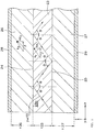
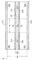
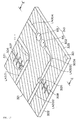
- In Fig. 1 a
dielectric substrate 23 has a predetermined thickness t23 and a predetermined width W20. On the top surface of thedielectric substrate 23,electrodes slot 24 having width W is formed between theelectrodes - The slot is located in the central portion of the
dielectric substrate 23 along its width and in parallel to the longitudinal direction of thesubstrate 23. Also, on the bottom surface of thedielectric substrate 23,electrodes slot 25 having the same width W as theslot 24 is formed between theelectrodes slot 25 is located in the central portion of thedielectric substrate 23 along its width and in parallel to the longitudinal direction of thesubstrate 23. Theslots dielectric substrate 23 interposed between theslots propagation region 23c in which a high-frequency signal having a desired propagation frequency fb is transmitted, as will be described below in a greater detail. - On the top surface of the
dielectric substrate 23 having theelectrodes dielectric substrate 26 with the same width W20 and length as thesubstrate 23 is provided. Anelectrode 28 is further mounted on the entire top surface of thedielectric substrate 26. Also, on the bottom surface of thedielectric substrate 23 having theelectrodes dielectric substrate 27 having the same width W20 and length as thedielectric substrate 23 is located. Anelectrode 29 is disposed on the entire bottom surface of thedielectric substrate 27. - The dielectric
constant ε r26 of thedielectric substrate 26 is set to be equal to the dielectricconstant ε r27 of thedielectric substrate 27. On the other hand, the dielectricconstant ε r23 of thedielectric substrate 23 is set larger than the dielectricconstant ε r26 andε r27, as will be explained below. - Fig. 2 shows a plane electromagnetic wave pw23 that is incident onto the top surface of the
dielectric substrate 23 in theslot 24 at an incidence angle Θ and is reflected at an reflection angle Θ equal to the incidence angle. The top surface of thedielectric substrate 23 in theslot 24 forms a boundary between thedielectric substrates dielectric substrate 23 in theslot 24, is incident onto the bottom surface of thedielectric substrate 23 in theslot 25 at an incident angle Θ and is reflected at an reflection angle Θ equal to the incidence angle. The bottom surface of thedielectric substrate 23 in theslot 25 constitutes a boundary between thedielectric substrates propagation region 23c of thedielectric substrate 23 while being repeatedly reflected alternately on the top surface of thedielectric substrate 23 in theslot 24 and on the bottom surface of thesubstrate 23 in theslot 25. An electromagnetic wave propagating in the TE mode will hereinafter be referred to as a "TE wave". - The angle Θ can be expressed by the
following equation 1 using the propagation constant k1 of the plane electromagnetic wave pw23 and the phase constant β of the TE wave propagating in the longitudinal direction of thedielectric substrate 23.
- If the incidence angle Θ is larger than the critical angle Θdc expressed by the
following equation 2, the electromagnetic wave pw23 is totally reflected on the top surface of thedielectric substrate 23 in theslot 24 and the bottom surface of thesubstrate 23 in theslot 25, thus propagating within thepropagation region 23c of thesubstrate 23 without being attenuated.
dielectric substrate 26 or thesubstrate 27, whereby the wave pw23 is attenuated. - The propagation constant k is determined by the frequency of the plane electromagnetic wave pw23 and the dielectric
constant ε r23 of thedielectric substrate 23. The phase constant β is defined by the frequency of the electromagnetic wave pw23, and the dielectricconstant ε r23 and the thickness t of thedielectric substrate 23. It will now be assumed that x, y and z axes are determined, as illustrated in Fig. 2, and that a TE wave travels along the z axis while having the constant y component of an electric field Ey. The propagation constant k1 of the planar wave propagating through thedielectric substrate 23 can be expressed by the following equation 3 utilizing the dielectricconstant ε r23 of thedielectric substrate 23.
- Similarly, the propagation constant k2 of the planar wave propagating through the
dielectric substrate 26 can be expressed by the following equation 4 utilizing the dielectricconstant ε r26 of the dielectric substrate 26: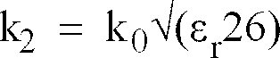
dielectric substrate 23 is equal to that in thedielectric substrate 26, the followingequation 5 can hold true:
dielectric substrates 
-
Equations 5 and 6 are solved to obtain the propagation constants kx1 and kx2 and the phase constant β. - The lower the frequency of the plane electromagnetic wave pw23 is, the smaller the incidence angle Θ is. Hence, as long as the frequency of the electromagnetic wave pw23 is not lower than the critical frequency fda at which the incidence angle Θ is equivalent to the critical angle Θdc, the wave will propagate through the
dielectric substrate 23 repeating the total reflection on the surface of thedielectric substrate 23 in theslot 24 and on the bottom surface of thesubstrate 23 in theslot 25. The dielectricconstant ε r23 and the thickness t23 of thedielectric substrate 23 and the dielectricconstant ε r26 andε r27 of thesubstrates constant ε r23 and the thickness t23 of thedielectric substrate 23 and the dielectricconstant ε r26 andε r27 of thesubstrates dielectric substrate 23 in theslot 24 and on the bottom surface of thesubstrate 23 close to theslot 25. - The
electrodes dielectric substrate 23, constitute a planar-parallel waveguide having a cut-off frequency substantially higher than the propagation frequency fb with respect to the TE wave. This forms a TE-wave cut-offregion 23a in thedielectric substrate 23. Likewise, theelectrodes region 23b along the width of thedielectric substrate 23 in a position opposite to the cut-offregion 23a. - Further, the
electrode 21a and the portion of theelectrode 28 facing each other constitute a planar-parallel waveguide. The thickness t26 of thesubstrate 26 is set so that the cut-off frequency with respect to the TE wave passing through the plane-parallel waveguide is substantially higher than the propagation frequency fb. Accordingly, a TE-wave cut-off region 26a is formed in thedielectric substrate 26. Similarly, theelectrode 21b and the portion of theelectrode 28 facing each other constitute a planar-parallel waveguide. A TE-wave cut-offregion 26b is thus formed in thedielectric substrate 26 in a position opposite to the cut-off region 26a. Moreover, in thedielectric substrate 27, a planar-parallel waveguide is defined by theelectrode 22a and the portion of theelectrode 29 opposedly facing each other. The thickness t27 of thedielectric substrate 27 is set so that the TE-wave cut-off frequency of the plane-parallel waveguide is substantially higher than the propagation frequency fb. This forms a TE-wave cut-offregion 27a in thedielectric substrate 27. Likewise, a TE-wave cut-offregion 27b is formed in thedielectric substrate 27, interposed between theelectrode 22b and theelectrode 29 opposedly facing each other, in a position opposite to the cut-offregion 27a. - In the planar dielectric line LN10 of the first embodiment, a
propagation region 23c is defined in which a high-frequency signal having a frequency not lower than the critical frequency fda repeats total reflection alternately on the top surface of thedielectric substrate 23 in theslot 24 and on the bottom surface of thesubstrate 23 in theslot 25. The cut-offregions dielectric substrate 23 of the dielectric line LN10 in the longitudinal direction while concentrating its electromagnetic-field energy inside and in the vicinity of thepropagation region 23c. - Also, since the planar dielectric line LN10 comprises the
dielectric substrates dielectric substrates - The planar dielectric line LN10 further comprises the
electrodes dielectric substrate 23 andelectrodes slots electrodes electrodes - Fig. 12 is a cross sectional view of a planar dielectric line LN20 according to a second embodiment of the present invention. The dielectric line LN20 differs from the dielectric line LN10 in that upper and lower
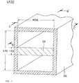
conductive plates dielectric substrate electrodes - On the top surface of the
substrate 23, theelectrodes slot 24. Also, on the bottom surface of thedielectric substrate 23,electrodes slot 25. The upper and lowerconductive plates dielectric substrate 23 provided with theslots conductive plates conductive plate 41a and the top surface of thesubstrate 23 is set to be equal to the distance between the lowerconductive plate 41b and the bottom surface of thesubstrate 23. - In the dielectric line LN20, the dielectric
constant ε r23 of thedielectric substrate 23 is determined as follows. The reflection of an electromagnetic wave on the top surface of thesubstrate 23 in theslot 24 and on the bottom surface of thesubstrate 23 in theslot 25 occurs, unlike the first embodiment, at a boundary between thedielectric substrate 23 and free space. The critical angle Θc can, therefore, be expressed by thefollowing equation 7 utilizing the dielectric constant εr = 1 of free space:
- Accordingly, in the planar dielectric line LN20 of this embodiment, the electromagnetic wave pw23 having a frequency not lower than the critical frequency fa at which the angle of reflection Θ becomes equal to the critical angle Θc propagates while repeating the total reflection on the top surface of the
dielectric substrate 23 in theslot 24 and on the bottom surface of thesubstrate 23 in theslot 25. The dielectricconstant ε r23 and the thickness t23 of thesubstrate 23 are set so that the propagation frequency fb is not lower than the critical frequency fa. - A plane-parallel waveguide is defined by the
electrode 21a and the upperconductive plate 41a opposedly facing each other. The spacing h41 between the upper and lowerconductive plates region 42a located between theelectrode 21a and the upperconductive plate 41a facing each other is thus formed in part of the free space interposed between thedielectric substrate 23 and the upperconductive plate 41a. Likewise, a plane-parallel waveguide is specified by theelectrode 21b and the upperconductive plate 41a facing each other. A TE-wave cut-offregion 42b between theelectrode 21b and the upperconductive plate 41a is thus formed in free space sandwiched between thesubstrate 23 and the upperconductive plate 41a, in a position opposite to the cut-offregion 42a. - As described above, the distance between the upper
conductive plate 41a and the top surface of thedielectric substrate 23 is determined equal to the distance between the lowerconductive plate 41b and the bottom surface of thesubstrate 23. Accordingly, a plane-parallel waveguide having a TE-wave cut-off frequency substantially higher than the propagation frequency fb is defined by theelectrode 22a and the lowerconductive plate 41b opposedly facing each other. A TE-wave cut-off region 43a clamped between theelectrode 22a and the lowerconductive plate 41b is thus formed in part of the free space interposed between thesubstrate 23 and the lowerconductive plate 41b. Similarly, a TE-wave cut-offregion 43b sandwiched between theelectrode 22b and the lowerconductive plate 41b facing each other is thus defined in the free space in a position opposite to the cut-off region 43a. - In the planar dielectric line LN20, a
propagation region 23c is constructed in which a high-frequency signal having a frequency not lower than the critical frequency fa is transmitted in thedielectric substrate 23 while repeating the total reflection alternately on the top surface of thesubstrate 23 in theslot 24 and on the bottom surface of thesubstrate 23 in theslot 25. On the other hand, in the cut-offregions propagation region 23c. - In the second embodiment, the upper and lower
conductive plates dielectric substrates - A detailed explanation will now be given of the principle of the operation of the dielectric line LN20 according to the second embodiment. Prior to an explanation of this line LN20, a dielectric-loaded waveguide line LN30 operated similar to the line LN20 will first be described.
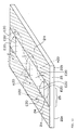
- The dielectric-loaded waveguide line LN30, as illustrated in Fig. 3, comprises a
square waveguide 36 having an internal width W36 and an internal height h36, and adielectric substrate 33 having a thickness t33 and a width equal to the width W36 of thewaveguide 36. Thedielectric substrate 33 is disposed at a central location with respect to the height of thesquare waveguide 36 so that it can be located in parallel to the upper and lower conductive plates of thewaveguide 36. The dielectricconstant ε r33 of thedielectric substrate 33 shall be set to equal the dielectricconstant ε r23 of thedielectric substrate 23 of the second embodiment. - A high-frequency signal having a frequency not lower than the critical frequency fa is input into the waveguide line LN30 shown in Fig. 3 and is propagated in the
substrate 33 in the longitudinal direction while concentrating its electromagnetic energy inside and in the proximity of thesubstrate 33. The electromagnetic-field distribution obtained during the propagation of the signal in thewaveguide 36 is indicated in Figs. 4A and 4B. Fig. 4A illustrates an electric field E30 and a magnetic field H30 in a cross sectional view along line C-C' of Fig. 3. Fig. 4B illustrates the electric field E30 and the magnetic field H30 in a longitudinal sectional view along line B-B' of Fig. 3. Figs. 4A and 4B clearly show that the electric field E30 and the magnetic field H30 are distributed inside and in the vicinity of thedielectric substrate 33. The electric field E30 has only a component in the widthwise direction of thesubstrate 33, while the magnetic field H30 has both a component in the longitudinal direction of thesubstrate 33, i.e., the longitudinal direction of thewaveguide 36, and a component perpendicular to the top surface or the bottom surface of thesubstrate 33. - In contrast, Figs. 11A and 11B illustrate an electromagnetic-field distribution obtained when a high-frequency signal having a frequency lower than the critical frequency fa is input into the dielectric-loaded waveguide line LN30. Fig. 11A illustrates the electric field E30 and the magnetic field H30 in a cross sectional view along line C-C' of Fig. 3. Fig. 11B illustrates the electric field E30 and the magnetic field H30 in a longitudinal sectional view along line B-B' of Fig. 3. As is seen from Fig. 11A and 11B, the magnetic field H30 is distributed farther away from the
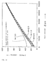
substrate 33 than the magnetic field of the frequency not lower than the critical frequency fa shown in Figs. 4A and 4B, and further, as seen in Fig. 11A, the electric field E30 has a component outside thesubstrate 33. - Fig. 5 is a diagram indicating the relation between the frequency and the phase constant β30 of the dielectric-loaded waveguide line LN30 when the dielectric
constant ε r33 of thesubstrate 33 was varied to have thevalues equations 5 and 6. The parameters of the structure of the waveguide line LN30 were set as follows: - (1) The thickness t33 of the
substrate 33 = 0.33 mm; and - (2) The height h36 of the
waveguide 36 = 2.25 mm - Fig. 5 reveals that a higher frequency causes a larger phase constant β30 and that a greater dielectric
constant ε r33 gives rise to a larger phase constant β30 under the condition of the same frequency. - Fig. 6 is a diagram representing the relation between the frequency and the phase constant β30 of the waveguide line LN30 obtained when the thickness t of the
substrate 33 was varied to have the values 0.1 mm, 0.33 mm, 0.5 mm and 1 mm. The values shown in Fig. 6 were calculated according toequations 5 and 6. The parameters of the structure of the waveguide line LN30 were set as follows: - (1) The dielectric
constant ε r33 of the substrate = 9.3; and - (2) The internal height h36 of the
waveguide 36 = 2.25 mm - Fig. 6 demonstrates that a greater thickness t33 of the
substrate 33 causes a greater phase constant β30 under the condition of the same frequency. - Next, the critical frequency fa at which the incidence angle Θ is equal to the critical angle Θc will be calculated with the use of the dielectric-loaded waveguide line LN30.
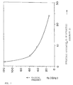
- Fig. 7 is a diagram indicating the relation between the critical frequency fa at which the incidence angle Θ is equal to the critical angle Θc and the dielectric
constant ε r33 of thesubstrate 33. The parameters of the structure of the waveguide line LN30 were set as follows: - (1) The thickness t33 of the
substrate 33 = 0.33 mm; - (2) The internal width W36 of the
waveguide 36 = 2.0 mm; and - (3) The internal height h36 of the
waveguide 36 = 2.25 mm. - As is seen from Fig. 7, a greater dielectric
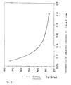
constant ε r33 of thesubstrate 33 brings about a lower critical frequency fa. Namely, with adielectric substrate 33 having a higher dielectricconstant ε r33, the minimum propagation frequency fb of a totally-reflecting high-frequency signal can be reduced to a lower level. - Fig. 8 is a diagram representing the relation between the critical frequency fa at which the incidence angle Θ is equal to the critical angle Θc and the thickness t33 of the
substrate 33. The parameters of the structure of the waveguide line LN30 were set as follows: - (1) The dielectric
constant ε r33 of thesubstrate 33 = 9.3; - (2) The internal width W36 of the
waveguide 36 = 2.0 mm; and - (3) The internal height h36 of the
waveguide 36 = 2.25 mm. - Fig. 8 reveals that a greater thickness t33 of the
substrate 33 causes a lower critical frequency fa at which the incidence angle Θ is equal to the critical angle Θc. That is, by increasing the thickness t33 of thesubstrate 33, the minimum propagation frequency fb of a totally reflecting high-frequency signal can be reduced to a lower level. - Based on the operation principle of the waveguide line LN30 explained above, the operation of the planar dielectric line LN20 (Fig. 12) of the second embodiment will now be described. The critical frequency fa of the dielectric line LN20 was calculated from the critical frequency fa of the dielectric line LN30 when the parameters of the line LN20 were set as follows:
- (1) The thickness t23 of the
substrate 23 = 0.33 mm; - (2) The width W20 of the
substrate 23 = 8 mm; and - (3) The widths W of the
slots - The dielectric
constant ε r23 and the thickness t23 of thesubstrate 23 are respectively set equal to the dielectricconstant ε r33 and the thickness t33 of thesubstrate 33. Also, the widths W of theslots substrate 23 are set equal to the internal width W of thewaveguide 36. The spacing h41 between the upper and lowerconductive plates waveguide 36. - Fig. 9 is a diagram designating the relation between the frequency and the phase constant β20 of the dielectric line LN20 when the dielectric
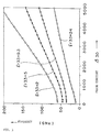
constant ε r23 of thesubstrate 23 was set at thevalues constant ε r23 brings about a greater phase constant β20 under the condition of the same frequency. - Fig. 10 is a diagram indicating the relation between the frequency and the phase constant β20 of the dielectric line LN20 when the widths W of the
slots substrate 23 were set at the values 0.5 mm, 1 mm, 2 mm and 3 mm. The values shown in Fig. 10 were calculated according to the finite-element method. The parameters of the structure of the dielectric line LN20 were set as follows: - (1) The dielectric
constant ε r23 of thesubstrate 23 = 9.3; - (2) The width W20 of the
substrate 23 = 8 mm; and - (3) The spacing h41 between the upper and mm. lower
conductive plates - Fig. 10 shows that a greater width W of the
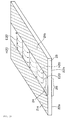
slots - A further explanation will further be given of the electromagnetic-field distribution of the dielectric line LN20 (Fig. 12) according to the second embodiment. Fig. 13 illustrates the electromagnetic-field distribution in a perspective view of the
dielectric substrate 23 as a comparative example when a high-frequency signal having a frequency lower than the critical frequency fa is input into the dielectric line LN20. In Fig. 13, the upper and lowerconductive plates dielectric substrate 23 is shown. Also in the perspective view of Fig. 13, the top portions of theelectrodes substrate 23 than the electromagnetic-field distribution achieved at a frequency not lower than the critical frequency fa, as shown in Fig. 14. - Fig. 14 illustrates the electromagnetic distribution when a high-frequency signal having a frequency not lower than the critical frequency fa is input into the dielectric line LN20.
- In Fig. 14, as well as Fig. 13, the upper and lower
conductive plates substrate 23 is shown. Also, in the perspective view of Fig. 14, the top surfaces of theelectrodes propagation region 23c of the substrate 23d. More specifically, it is seen that a high-frequency signal having a frequency not lower than the critical frequency fa is totally reflected by top surface of thesubstrate 23 adjacent to theslot 24 and by the bottom surface of thesubstrate 23 in the vicinity of theslot 25. - Although only the operation of the dielectric line L20 has been discussed above, the dielectric line LN10 of the first embodiment is operated in a manner similar to the line LN20. As has been described above in detail, both the planar dielectric line LN10 of the first embodiment and the line LN20 of the second embodiment are operated in a manner similar to the dielectric-loaded waveguide line LN30 and used for transmitting a high-frequency signal having a frequency not lower than the critical frequency fa.
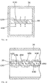
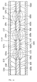
- The present inventors observed the electric-field distribution by use of the model shown in Fig. 15 in order to examine the operation performed when two or more planar dielectric lines are disposed in proximity to each other. The construction of the model and results will be explained. In the model shown in Fig. 15, the
electrodes slots slot 124a is disposed between theelectrodes slot 124b is located between theelectrodes slot 124c is interposed between theelectrodes slots substrate 23 and also have the same widths. Theelectrodes - Mounted on the bottom surface of the
substrate 123 areelectrodes electrodes substrate 123. Also,electrodes electrodes substrate 123. With this arrangement,slots slots substrate 123 is disposed between the upper and lower conductive plates 141a and 141b in parallel to each other so that it can be placed in parallel thereto. The distance between the top surface of thesubstrate 123 and the upper conductive plate 141a can be equal to the distance between the bottom surface of thesubstrate 123 and the lower conductive plate 141b. Moreover, the upper and lower conductive plates 141a and 141b are spaced apart from each other in a manner similar to the second embodiment. The three planar dielectric lines in parallel to each other are thus constructed. - Fig. 15 illustrates an electric field E120 obtained when high-frequency signals having a frequency not lower than the critical frequency fa are transmitted in the three plane dielectric lines. Fig. 15 shows that the signals are transmitted in the longitudinal direction of the
substrate 123 without interfering with each other. Fig. 16 indicates an electric field E12 resulting when high-frequency signals having a frequency lower than the critical frequency fa are transmitted in the three lines. Fig. 16 reveals that high-frequency signals suffer from electromagnetic-field coupling, i.e., electromagnetic-field interference. - As has been discussed above in detail, in the respective planar dielectric lines LN10 and LN20 of the first and second embodiments, a high-frequency signal having a frequency not lower than the critical frequency fa is totally reflected on the top surface of the
substrate 23 adjacent to theslot 24 and on the bottom surface of thesubstrate 23 in the vicinity of theslot 25, whereby the signal can be propagated while concentrating its electromagnetic-field energy inside and in the proximity of thepropagation region 23c of thesubstrate 23. To further develop these embodiments, it is possible to dispose a plurality of planar dielectric lines in parallel to each other along the width of thesubstrate 123, thus enabling the formation of highly-integrated circuits. - Fig. 17 is a perspective view of an integrated circuit produced by the application of the planar dielectric line according to the present invention. This integrated circuit is configured to have a generally-square
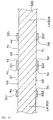
dielectric substrate 323 provided with a plurality of dielectric lines. Anelectrode 321 with a predetermined shape is mounted on the top surface of thesubstrate 323, while anelectrode 322 with a predetermined shape is formed on the bottom surface of thesubstrate 323, both theelectrodes high pass filter 310, and biasinglines dielectric substrate 323. On the top surface of thesubstrate 323, acircuit part module 305 is connected between the dielectric lines LN302 and LN303, while acircuit part module 306 is connected between the dielectric line LN301 and thebiasing line 307. The bent portions of the lines LN301 and LN303 are comprised ofline portions 301a and 303a, respectively, formed by the narrowed slots. This makes it possible to bend the dielectric lines LN301 and LN303 without requiring a change from the propagation mode currently employed in the lines LN301 and LN303 to another mode. - The
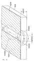
high pass filter 310 will now be described. Fig. 18 is a sectional view along line E-E' of Fig. 17. As shown in Figs. 17 and 18, twocircular openings substrate 323. On the other hand, twocircular openings openings substrate 323. Theopenings openings regions resonator region 66, which is part of thesubstrate 323, is defined as a cylindrical region having thesurface 67 of theopening 4c in thesubstrate 323 and thesurface 68 of theopening 5c in thesubstrate 323. Theresonator region 69, on the other hand, which is part of thesubstrate 323, is defined as a cylindrical region having thesurface 70 of theopening 4d in thesubstrate 323 and thesurface 71 of theopening 5d in thesubstrate 323. - The dielectric constant and the thickness of the
substrate 323 and the diameters of theopenings resonator regions resonator regions electrodes substrate 323 are also determined so that the cut-off frequency of the plane-parallel waveguide will be higher than a desired resonance frequency. With this arrangement, theresonator region 66 and adjacent free space, and theresonator region 69 and free space in the vicinity thereof, respectively constitute TE010 mode-dielectric resonators. Theregions region 66 can be inductively coupled. The distance between the dielectric line LN304 and theregion 69 is determined so that the dielectric line LN304 and the TE010 mode-dielectric resonator formed by theregion 69 can be inductively coupled. - In this manner, the
high pass filter 310 is constructed by the cascade connection of the two TE010 mode dielectric resonators between the dielectric lines LN303 and LN304. This causes a high-frequency signal having a predetermined frequency passing through the dielectric line LN303 being transmitted to the line LN304 through the two TE010 mode-dielectric resonators. - Examples of modifications of the present invention will now be explained.
- The planar dielectric line LN10 of the first embodiment is comprised of the
dielectric substrates conductive plates dielectric substrate 23 provided with theslots - Although the upper and lower
conductive plates - Instead, a square waveguide defined by the upper and lower
conductive plates - In the dielectric line LN20 of the second embodiment, the distance between the upper
conductive plate 41a and the top surface of thesubstrate 23 is determined to equal the distance between the lowerconductive plate 41b and the bottom surface of thesubstrate 23. However, this is not exclusive, and the former distance may differ from the latter distance. The line obtained by the above modification is still operable in a manner similar to the first and second embodiments and can present the similar advantages. - Further, although the dielectric
constant ε r26 of thedielectric substrate 26 is determined to be equal to the dielectricconstant ε r27 of thesubstrate 27, they may differ from each other. - As will be clearly understood from the foregoing description, the present invention offers the following advantages.
- In the planar dielectric line according to a first aspect of the present invention, a first slot having a predetermined width is formed on the first surface of the dielectric substrate, and a second slot is mounted on the second surface of the substrate, both the slots facing each other. This makes it possible to provide a small and inexpensive planar dielectric line that can enhance easier connection with electronic parts, such as ICs, and inhibit conductor losses to a lower level than microstrip lines, coplanar lines and slotted lines.
- The planar dielectric line according to a second aspect of the present invention is constructed by adding first and second conductive plates to the planar dielectric line implemented by the first aspect of the present invention. It is thus possible to prevent leakage to the exterior of high-frequency signals propagating in the above-described dielectric line and also to preclude the entry of high-frequency signals from the exterior of the dielectric line.
- In the planar dielectric line according to a third aspect of the present invention, the following features are added to the dielectric line implemented by the second aspect of the present invention. Namely, a dielectric is charged between the first surface of the dielectric substrate and the first conductive plate, and another dielectric is interposed between the second surface of the substrate and the second conductive plate, each dielectric having a smaller degree of permittivity than the dielectric substrate. The planar dielectric line can thus be made thinner.
- An integrated circuit according to a fourth aspect of the present invention comprises a transmission line and a high-frequency device connected to the transmission line. The transmission line includes at least one of the planar dielectric lines implemented by the first to third aspects of the present invention. Accordingly, a highly-integrated circuit can be constructed.
Claims (6)
- A planar dielectric line comprising:a dielectric substrate (23) having first and second surfaces which opposedly face each other;a first slot (24) having a predetermined width (w) and being interposed between first and second electrodes (21a,21b), said first and second electrodes (21a,21b) being formed on the first surface of said dielectric substrate (23) and opposedly facing each other across a predetermined spacing to define said first slot (24); anda second slot (25) having substantially the same width (w) as said first slot (24) and being interposed between third and fourth electrodes (22a,22b), said second slot (25) opposedly facing said first slot (24), said third and fourth electrodes (22a,22b) being formed on the second surface of said dielectric substrate (23) and opposedly facing each other across a predetermined spacing, to define said second slot (25),wherein the dielectric constant and the thickness of said dielectric substrate (23) are determined so that a plane electromagnetic wave having at least a predetermined frequency and propagating in a propagation region of said dielectric substrate (23) interposed between said first and second slots (24,25) is totally reflected by the first and second surfaces of said dielectric substrate (23) in said first and second slots (24,25), respectively.
- A planar dielectric line according to claim 1, further comprising:a first conductive plate (28) disposed away from the first surface of said dielectric substrate (23) across a predetermined distance; anda second conductive plate (29) disposed away from the second surface of said dielectric substrate (23) across a predetermined distance.
- A planar dielectric line according to claim 2, wherein a dielectric (26,27) is interposed between the first surface of said dielectric substrate (23) and said first conductive plate (28) and between the second surface of said dielectric substrate (23) and said second conductive plate (29), said dielectric (26,27) having a lower dielectric constant than that of said dielectric substrate (23).
- An integrated circuit comprising:a transmission line; anda high-frequency device connected to said transmission line,said transmission line including:a dielectric substrate (23) having first and second surfaces which opposedly face each other;a first slot (24) having a predetermined width (w) and being interposed between first and second electrodes (21a,21b), said first and second electrodes (21a,21b) being formed on the first surface of said dielectric substrate (23) opposedly facing each other across a predetermined spacing to define said first slot (24); anda second slot (25) having substantially the same width (w) as said first slot (24) and being interposed between third and fourth electrodes (22a,22b), said second slot (25) opposedly facing said first slot (24), said third and fourth electrodes (22a,22b) being formed on the second surface of said dielectric substrate (23) opposedly facing each other across a predetermined spacing to define said second slot (25),wherein the dielectric constant and the thickness of said dielectric substrate (23) are determined in such a manner that a plane electromagnetic wave having at least a predetermined frequency propagating in a propagation region of said dielectric substrate (23) interposed between said first and second slots (24,25) is totally reflected by the first and second surfaces of said dielectric substrate (23) in said first and second slots (24,25), respectively.
- An integrated circuit according to claim 4, wherein said transmission line further includes:a first conductive plate (28) disposed away from the first surface of said dielectric substrate (23) across a predetermined distance; anda second conductive plate (29) disposed away from the second surface of said dielectric substrate (23) across a predetermined distance.
- An integrated circuit according to claim 5, wherein a dielectric (26,27) is interposed between the first surface of said dielectric substrate (23) and said first conductive plate (28) and between the second surface of said dielectric substrate (23) and said second conductive plate (29), said dielectric (26,27) having a lower dielectric constant than that of said dielectric substrate (23).
Applications Claiming Priority (3)
| Application Number | Priority Date | Filing Date | Title |
|---|---|---|---|
| JP69867/95 | 1995-03-28 | ||
| JP6986795 | 1995-03-28 | ||
| JP7069867A JP2991076B2 (en) | 1995-03-28 | 1995-03-28 | Planar dielectric line and integrated circuit |
Publications (2)
| Publication Number | Publication Date |
|---|---|
| EP0735604A1 true EP0735604A1 (en) | 1996-10-02 |
| EP0735604B1 EP0735604B1 (en) | 2003-02-26 |
Family
ID=13415181
Family Applications (1)
| Application Number | Title | Priority Date | Filing Date |
|---|---|---|---|
| EP96104889A Expired - Lifetime EP0735604B1 (en) | 1995-03-28 | 1996-03-27 | Planar dielectric line and integrated circuit using the same |
Country Status (6)
| Country | Link |
|---|---|
| EP (1) | EP0735604B1 (en) |
| JP (1) | JP2991076B2 (en) |
| KR (1) | KR0177909B1 (en) |
| CN (2) | CN1226805C (en) |
| CA (1) | CA2172888C (en) |
| DE (1) | DE69626332T2 (en) |
Cited By (5)
| Publication number | Priority date | Publication date | Assignee | Title |
|---|---|---|---|---|
| EP0871239A1 (en) * | 1997-04-10 | 1998-10-14 | Murata Manufacturing Co., Ltd. | Antenna device and radar module |
| EP0862215A3 (en) * | 1997-02-27 | 1999-09-29 | Murata Manufacturing Co., Ltd. | Planar dielectric integrated circuit |
| EP0862216A3 (en) * | 1997-02-27 | 1999-10-06 | Murata Manufacturing Co., Ltd. | Planar dielectric integrated circuit |
| EP0883204A3 (en) * | 1997-06-05 | 1999-11-17 | Murata Manufacturing Co., Ltd. | Nonradiative planar dielectric line and integrated circuit using the same line |
| US6166614A (en) * | 1997-04-03 | 2000-12-26 | Murata Manufacturing Co., Ltd. | Nonradiative planar dielectric line and integrated circuit |
Families Citing this family (9)
| Publication number | Priority date | Publication date | Assignee | Title |
|---|---|---|---|---|
| JP3678194B2 (en) | 2001-12-04 | 2005-08-03 | 株式会社村田製作所 | Transmission line and transmission / reception device |
| JP3695395B2 (en) | 2002-01-09 | 2005-09-14 | 株式会社村田製作所 | Transmission line and transmission / reception device |
| US7365618B2 (en) | 2005-12-06 | 2008-04-29 | Murata Manufacturing Co., Ltd. | High-frequency circuit device, high-frequency module, and communication apparatus |
| US9478840B2 (en) * | 2012-08-24 | 2016-10-25 | City University Of Hong Kong | Transmission line and methods for fabricating thereof |
| JP6279977B2 (en) * | 2014-06-02 | 2018-02-14 | モレックス エルエルシー | Waveguide |
| CN112738985B (en) * | 2021-02-04 | 2022-04-08 | 华勤技术股份有限公司 | Circuit board assembly and electronic equipment |
| CN115144962B (en) * | 2021-03-31 | 2024-02-06 | 南京星隐科技发展有限公司 | Electromagnetic wave transmission structure, device and optical chip |
| WO2022205124A1 (en) * | 2021-03-31 | 2022-10-06 | 南京星隐科技发展有限公司 | Electromagnetic wave transmission structure, device, and optical chip |
| CN114552155B (en) * | 2022-04-25 | 2022-07-05 | 电子科技大学成都学院 | Dual-mode transmission line |
Citations (3)
| Publication number | Priority date | Publication date | Assignee | Title |
|---|---|---|---|---|
| US3026490A (en) * | 1959-12-28 | 1962-03-20 | Bell Telephone Labor Inc | Microwave coupling arrangements |
| EP0040067A1 (en) * | 1980-05-12 | 1981-11-18 | Junkosha Co. Ltd. | Strip line cable |
| EP0244105A2 (en) * | 1986-04-16 | 1987-11-04 | Hewlett-Packard Company | Integrated capacitance structures in microwave finline devices |
Family Cites Families (1)
| Publication number | Priority date | Publication date | Assignee | Title |
|---|---|---|---|---|
| JP5345509B2 (en) | 2009-11-22 | 2013-11-20 | 日本ポリプロ株式会社 | Polypropylene resin composition for packaging film of heat sterilized food, and film for packaging of heat sterilized food obtained using the same |
-
1995
- 1995-03-28 JP JP7069867A patent/JP2991076B2/en not_active Expired - Lifetime
-
1996
- 1996-03-27 DE DE69626332T patent/DE69626332T2/en not_active Expired - Lifetime
- 1996-03-27 EP EP96104889A patent/EP0735604B1/en not_active Expired - Lifetime
- 1996-03-28 CN CNB031462995A patent/CN1226805C/en not_active Expired - Lifetime
- 1996-03-28 CA CA002172888A patent/CA2172888C/en not_active Expired - Lifetime
- 1996-03-28 CN CN96107349A patent/CN1120542C/en not_active Expired - Lifetime
- 1996-03-28 KR KR1019960008848A patent/KR0177909B1/en not_active Expired - Lifetime
Patent Citations (3)
| Publication number | Priority date | Publication date | Assignee | Title |
|---|---|---|---|---|
| US3026490A (en) * | 1959-12-28 | 1962-03-20 | Bell Telephone Labor Inc | Microwave coupling arrangements |
| EP0040067A1 (en) * | 1980-05-12 | 1981-11-18 | Junkosha Co. Ltd. | Strip line cable |
| EP0244105A2 (en) * | 1986-04-16 | 1987-11-04 | Hewlett-Packard Company | Integrated capacitance structures in microwave finline devices |
Non-Patent Citations (2)
| Title |
|---|
| H.C.C. FERNANDES ET AL.: "Metallization thickness in bilateral and unilateral finlines", INTERNATIONAL JOURNAL OF INFRARED AND MILLIMETER WAVES, vol. 15, no. 6, June 1994 (1994-06-01), NEW YORK US, pages 1001 - 1014, XP000454389 * |
| J.J. LEE: "Slotline impedance", IEEE TRANSACTIONS ON MICROWAVE THEORY AND TECHNIQUES, vol. 39, no. 4, April 1991 (1991-04-01), NEW YORK US, pages 666 - 672, XP000179063 * |
Cited By (9)
| Publication number | Priority date | Publication date | Assignee | Title |
|---|---|---|---|---|
| EP0862215A3 (en) * | 1997-02-27 | 1999-09-29 | Murata Manufacturing Co., Ltd. | Planar dielectric integrated circuit |
| EP0862216A3 (en) * | 1997-02-27 | 1999-10-06 | Murata Manufacturing Co., Ltd. | Planar dielectric integrated circuit |
| US6169301B1 (en) | 1997-02-27 | 2001-01-02 | Murata Manufacturing Co., Ltd. | Planar dielectric integrated circuit |
| US6445255B1 (en) | 1997-02-27 | 2002-09-03 | Murata Manufacturing Co., Ltd. | Planar dielectric integrated circuit |
| US6717492B2 (en) * | 1997-02-27 | 2004-04-06 | Murata Manufacturing Co., Ltd. | Planar dielectric integrated circuit with line conversion conductor patterns |
| US6166614A (en) * | 1997-04-03 | 2000-12-26 | Murata Manufacturing Co., Ltd. | Nonradiative planar dielectric line and integrated circuit |
| EP0871239A1 (en) * | 1997-04-10 | 1998-10-14 | Murata Manufacturing Co., Ltd. | Antenna device and radar module |
| US6052087A (en) * | 1997-04-10 | 2000-04-18 | Murata Manufacturing Co., Ltd. | Antenna device and radar module |
| EP0883204A3 (en) * | 1997-06-05 | 1999-11-17 | Murata Manufacturing Co., Ltd. | Nonradiative planar dielectric line and integrated circuit using the same line |
Also Published As
| Publication number | Publication date |
|---|---|
| CN1144406A (en) | 1997-03-05 |
| KR960036193A (en) | 1996-10-28 |
| DE69626332T2 (en) | 2003-11-27 |
| CN1479406A (en) | 2004-03-03 |
| CA2172888C (en) | 2005-05-24 |
| JPH08265007A (en) | 1996-10-11 |
| CA2172888A1 (en) | 1996-09-29 |
| JP2991076B2 (en) | 1999-12-20 |
| KR0177909B1 (en) | 1999-05-15 |
| CN1226805C (en) | 2005-11-09 |
| EP0735604B1 (en) | 2003-02-26 |
| CN1120542C (en) | 2003-09-03 |
| DE69626332D1 (en) | 2003-04-03 |
Similar Documents
| Publication | Publication Date | Title |
|---|---|---|
| US5986527A (en) | Planar dielectric line and integrated circuit using the same line | |
| KR100292763B1 (en) | Antenna device and radar module | |
| EP1049192B1 (en) | High-frequency communication device | |
| US6870438B1 (en) | Multi-layered wiring board for slot coupling a transmission line to a waveguide | |
| US7154441B2 (en) | Device for transmitting or emitting high-frequency waves | |
| EP0735604B1 (en) | Planar dielectric line and integrated circuit using the same | |
| JP2004153367A (en) | High frequency module, and mode converting structure and method | |
| EP0898322B1 (en) | Dielectric waveguide line and its branch structure | |
| US12489187B2 (en) | Microwave system and apparatus | |
| CN110098485A (en) | Small spacing micro-strip antenna array | |
| KR101812490B1 (en) | Designs and methods to implement surface mounting structures of SIW | |
| JP2005051331A (en) | Coupling structure of microstrip line and dielectric waveguide | |
| Yamazaki et al. | Broadband differential-line-to-waveguide transition in multi-layer dielectric substrates with an X-shaped patch element in 280 GHz band | |
| JPH11340701A (en) | Connection structure of high-frequency transmission line | |
| JP3013798B2 (en) | Crossing track | |
| US6727776B2 (en) | Device for propagating radio frequency signals in planar circuits | |
| US6535089B1 (en) | High-frequency circuit device and communication apparatus using the same | |
| EP0883204B1 (en) | Nonradiative planar dielectric line and integrated circuit using the same line | |
| US6166614A (en) | Nonradiative planar dielectric line and integrated circuit | |
| US10651524B2 (en) | Planar orthomode transducer | |
| JP2000077912A (en) | Connection structure of dielectric waveguide line | |
| JP7113986B2 (en) | Converter and antenna device | |
| WO2011136737A1 (en) | Silicon based millimeter wave waveguide transition | |
| Chokchai et al. | Broadband GCPW-to-Waveguide Transition in Multi-Layer Dielectric Substrate with Double Patch and Corrugation Structures in 275 GHz Band | |
| Yuasa et al. | Simple design formula for parallel plate mode suppression by ground via-holes in multi-layered packages |
Legal Events
| Date | Code | Title | Description |
|---|---|---|---|
| PUAI | Public reference made under article 153(3) epc to a published international application that has entered the european phase |
Free format text: ORIGINAL CODE: 0009012 |
|
| 17P | Request for examination filed |
Effective date: 19960327 |
|
| AK | Designated contracting states |
Kind code of ref document: A1 Designated state(s): DE FI FR GB NL SE |
|
| 17Q | First examination report despatched |
Effective date: 20000204 |
|
| GRAH | Despatch of communication of intention to grant a patent |
Free format text: ORIGINAL CODE: EPIDOS IGRA |
|
| GRAH | Despatch of communication of intention to grant a patent |
Free format text: ORIGINAL CODE: EPIDOS IGRA |
|
| GRAA | (expected) grant |
Free format text: ORIGINAL CODE: 0009210 |
|
| AK | Designated contracting states |
Designated state(s): DE FI FR GB NL SE |
|
| PG25 | Lapsed in a contracting state [announced via postgrant information from national office to epo] |
Ref country code: NL Free format text: LAPSE BECAUSE OF FAILURE TO SUBMIT A TRANSLATION OF THE DESCRIPTION OR TO PAY THE FEE WITHIN THE PRESCRIBED TIME-LIMIT Effective date: 20030226 Ref country code: FI Free format text: LAPSE BECAUSE OF FAILURE TO SUBMIT A TRANSLATION OF THE DESCRIPTION OR TO PAY THE FEE WITHIN THE PRESCRIBED TIME-LIMIT Effective date: 20030226 |
|
| REG | Reference to a national code |
Ref country code: GB Ref legal event code: FG4D |
|
| REF | Corresponds to: |
Ref document number: 69626332 Country of ref document: DE Date of ref document: 20030403 Kind code of ref document: P |
|
| PG25 | Lapsed in a contracting state [announced via postgrant information from national office to epo] |
Ref country code: SE Free format text: LAPSE BECAUSE OF FAILURE TO SUBMIT A TRANSLATION OF THE DESCRIPTION OR TO PAY THE FEE WITHIN THE PRESCRIBED TIME-LIMIT Effective date: 20030526 |
|
| NLV1 | Nl: lapsed or annulled due to failure to fulfill the requirements of art. 29p and 29m of the patents act | ||
| ET | Fr: translation filed | ||
| PLBE | No opposition filed within time limit |
Free format text: ORIGINAL CODE: 0009261 |
|
| STAA | Information on the status of an ep patent application or granted ep patent |
Free format text: STATUS: NO OPPOSITION FILED WITHIN TIME LIMIT |
|
| 26N | No opposition filed |
Effective date: 20031127 |
|
| REG | Reference to a national code |
Ref country code: FR Ref legal event code: PLFP Year of fee payment: 20 |
|
| PGFP | Annual fee paid to national office [announced via postgrant information from national office to epo] |
Ref country code: DE Payment date: 20150324 Year of fee payment: 20 |
|
| PGFP | Annual fee paid to national office [announced via postgrant information from national office to epo] |
Ref country code: FR Payment date: 20150309 Year of fee payment: 20 Ref country code: GB Payment date: 20150325 Year of fee payment: 20 |
|
| REG | Reference to a national code |
Ref country code: DE Ref legal event code: R071 Ref document number: 69626332 Country of ref document: DE |
|
| REG | Reference to a national code |
Ref country code: GB Ref legal event code: PE20 Expiry date: 20160326 |
|
| PG25 | Lapsed in a contracting state [announced via postgrant information from national office to epo] |
Ref country code: GB Free format text: LAPSE BECAUSE OF EXPIRATION OF PROTECTION Effective date: 20160326 |