EP0732869A2 - Verfahren und Schaltungsanordnung zum Betrieb einer Entladungslampe - Google Patents
Verfahren und Schaltungsanordnung zum Betrieb einer Entladungslampe Download PDFInfo
- Publication number
- EP0732869A2 EP0732869A2 EP96103407A EP96103407A EP0732869A2 EP 0732869 A2 EP0732869 A2 EP 0732869A2 EP 96103407 A EP96103407 A EP 96103407A EP 96103407 A EP96103407 A EP 96103407A EP 0732869 A2 EP0732869 A2 EP 0732869A2
- Authority
- EP
- European Patent Office
- Prior art keywords
- period
- discharge lamp
- lamp
- current
- operating
- Prior art date
- Legal status (The legal status is an assumption and is not a legal conclusion. Google has not performed a legal analysis and makes no representation as to the accuracy of the status listed.)
- Granted
Links
Images


Classifications
-
- H—ELECTRICITY
- H05—ELECTRIC TECHNIQUES NOT OTHERWISE PROVIDED FOR
- H05B—ELECTRIC HEATING; ELECTRIC LIGHT SOURCES NOT OTHERWISE PROVIDED FOR; CIRCUIT ARRANGEMENTS FOR ELECTRIC LIGHT SOURCES, IN GENERAL
- H05B41/00—Circuit arrangements or apparatus for igniting or operating discharge lamps
- H05B41/14—Circuit arrangements
- H05B41/26—Circuit arrangements in which the lamp is fed by power derived from dc by means of a converter, e.g. by high-voltage dc
- H05B41/28—Circuit arrangements in which the lamp is fed by power derived from dc by means of a converter, e.g. by high-voltage dc using static converters
- H05B41/288—Circuit arrangements in which the lamp is fed by power derived from dc by means of a converter, e.g. by high-voltage dc using static converters with semiconductor devices and specially adapted for lamps without preheating electrodes, e.g. for high-intensity discharge lamps, high-pressure mercury or sodium lamps or low-pressure sodium lamps
- H05B41/2881—Load circuits; Control thereof
- H05B41/2882—Load circuits; Control thereof the control resulting from an action on the static converter
- H05B41/2883—Load circuits; Control thereof the control resulting from an action on the static converter the controlled element being a DC/AC converter in the final stage, e.g. by harmonic mode starting
-
- H—ELECTRICITY
- H05—ELECTRIC TECHNIQUES NOT OTHERWISE PROVIDED FOR
- H05B—ELECTRIC HEATING; ELECTRIC LIGHT SOURCES NOT OTHERWISE PROVIDED FOR; CIRCUIT ARRANGEMENTS FOR ELECTRIC LIGHT SOURCES, IN GENERAL
- H05B41/00—Circuit arrangements or apparatus for igniting or operating discharge lamps
- H05B41/14—Circuit arrangements
- H05B41/36—Controlling
- H05B41/38—Controlling the intensity of light
- H05B41/382—Controlling the intensity of light during the transitional start-up phase
- H05B41/388—Controlling the intensity of light during the transitional start-up phase for a transition from glow to arc
-
- Y—GENERAL TAGGING OF NEW TECHNOLOGICAL DEVELOPMENTS; GENERAL TAGGING OF CROSS-SECTIONAL TECHNOLOGIES SPANNING OVER SEVERAL SECTIONS OF THE IPC; TECHNICAL SUBJECTS COVERED BY FORMER USPC CROSS-REFERENCE ART COLLECTIONS [XRACs] AND DIGESTS
- Y02—TECHNOLOGIES OR APPLICATIONS FOR MITIGATION OR ADAPTATION AGAINST CLIMATE CHANGE
- Y02B—CLIMATE CHANGE MITIGATION TECHNOLOGIES RELATED TO BUILDINGS, e.g. HOUSING, HOUSE APPLIANCES OR RELATED END-USER APPLICATIONS
- Y02B20/00—Energy efficient lighting technologies, e.g. halogen lamps or gas discharge lamps
Definitions
- the invention relates to a method for operating a discharge lamp according to the preamble of claim 1 and a circuit arrangement for carrying out the method according to claim 7.
- discharge lamps in particular high-pressure discharge lamps
- the lamp already has an alternating voltage with the nominal frequency, for example 90-150 Hz, during start-up operation is fed. Ignition pulses are superimposed on this AC voltage.
- the lamp voltage and lamp current are reversed at the latest after half a period of the nominal frequency.
- the polarity reversal takes place after 5.5 ms.
- the electrodes have a temperature that does not allow thermal emission of electrodes. With the polarity reversal of the lamp voltage and the lamp current mentioned, the lamp tends to go out again or else it burns for a few milliseconds with a relatively high operating voltage of about 150-250 V in a glow discharge.
- a glow discharge has several disadvantages. On the one hand, a glow discharge leads to considerable material removal from the respective cathode. On the other hand, the material removal caused by the glow discharge leads to a blackening of the lamp bulb. In addition, this blackening causes a drop in luminous flux. These undesirable effects of a glow discharge occur with every polarity reversal process, as long as the electrodes have not yet reached their emission temperature.
- the object of the invention is to provide a method of the type mentioned at the outset and a corresponding circuit arrangement which enable a discharge lamp to be started up, in which the likelihood of the occurrence of glow discharges is reduced or in which the periods of time in which glow discharges occur can be shortened.
- the method according to the invention and the circuit arrangement according to the invention have several advantages.
- the likelihood of glow discharge occurring is reduced.
- Discharge lamps in particular high-pressure discharge lamps, are supplied with an alternating voltage with the nominal frequency at the start of operation (time t o ) in the prior art.
- This is shown schematically in FIG. 1, the lamp voltage U L (with 200 V / unit) being shown in the upper part of FIG. 1 and the lamp current I L (with 2A / unit) in the lower part of FIG. 1.
- a voltage U L with the nominal frequency is supplied to the lamp from the time (t o ) when it is switched on.
- ignition pulses in a time period T1.
- the firing pulses have an amplitude of 4 to 4.5 KV and a width of 1-2 microseconds, so that the firing pulses are not shown in FIG.
- FIG. 2 shows schematically the voltage and current supply according to the method according to the invention, the lamp voltage U L (with 200 V / unit) in the upper part of FIG. 2 and the lamp current I L (with 2A / unit) in the lower part of FIG. is shown.
- a direct voltage U 1 with an amplitude of typically 280 to 350 volts is applied to the discharge lamp. Ignition pulses are superimposed on this DC voltage U 1 until the lamp breaks through, ie ignites (time t1). The ignition pulses are not shown in FIG. 2 for the reasons that have been described in connection with FIG. 1. No lamp current flows in period T1.
- the period T1 lasts, for example, only 1 ms.
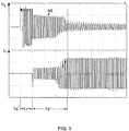
- Figure 3 shows the period T1 in an enlarged view
- the period T2 begins with the ignition.
- the discharge lamp is operated with a direct current I2 in a first direction.
- the voltage is typically 10 to 20 volts.
- the period T2 is typically 300-500 ms (in FIG. 2: approx. 350 ms).
- the direct current I2 is typically 1.5 times the nominal current, that is to say the current in the nominal operating state (following T4), in particular 1.5 to 2 times the nominal current.
- the period T3 begins after the period T2.
- the discharge lamp is operated with a direct current I3 in a second direction, which is opposite to the first direction.
- the voltage is also typically 10 to 20 volts.
- T3 is shorter than T2; in particular, the time period T3 is 100-200 ms (in FIG. 2: approx. 110 ms).
- the direct current I3 is also typically 1.5 times the nominal current, that is to say the current in the nominal operating state (following T4), in particular 1.5 to 2 times the nominal current.
- the discharge lamp impressed with an alternating current with the nominal frequency which continues to be at least 1.5 times the nominal current.
- the AC voltage is still typically 10 to 20 volts.
- the lamp voltage increases from 10 to 20 volts to its nominal value of e.g. 80 to 100 volts and the lamp current drops to the nominal value of e.g. 1.8 A in a 150 watt lamp.
- the period T4 which depends, among other things, on the ratio of the starting current to the nominal current (in the present case: factor 1.5 to 2), takes about 1 to 2 minutes.
- the second predefinable period T2 is selected so that the lamp electrode, which is anode during this period, is heated to the temperature (e.g. 2000 ° K) at which the thermal emission of electrons begins.
- the third predefinable period T3 is selected so that the lamp electrode, which is anode during this period T3 (in T2: cathode), is heated to the temperature (e.g. 2000 ° K) at which the thermal emission of electrons begins.
- the third predeterminable period T3 is shorter than the second predeterminable period T2.
- the lamp current can be higher during the second and / or third period T2, T3 than the lamp current subsequently formed in the period T4.
- the lamp current during the periods T2, T3 is at least 1.5 times higher than the lamp current subsequently formed.
- the circuit shown in FIG. 4 represents an example of a circuit arrangement for carrying out the method according to the invention, which forms part of an electronic ballast.
- This circuit arrangement is divided into the following blocks: power supply SV, full bridge VB, bridge driver BT, ignition Z, and control part C.
- the first four blocks SV, VB, BT and Z can be constructed identically to corresponding blocks in conventional circuit arrangements.
- the circuit arrangement has a control part which, for example, can be constructed like arrangement C shown in FIG.
- the control part C has a sensor S and timing elements ZG1, ZG2, ZG3 and ZG4, the sensor S being connected directly upstream of the timing element ZG2, which forms the period T2.
- the sensor S is used to detect the amount of the lamp voltage and consists of resistors R9, R10 and R11 and a capacitor C7.
- the lamp voltage tapped off via the voltage divider R9, R10, R11 is supplied to the timing element ZG2 via a diode D5, the circuit design and mode of operation of which are still to be described.
- the timing element ZG1 consists of a capacitor C6: an opposing stand R13, two diodes (in the block shown in dashed lines) D8 and a Schmitt trigger ST1. It is used to initialize the BT bridge driver, which works as follows:
- the capacitor C6 Before the operating voltage is switched on, the capacitor C6 is discharged (0 volt).
- the output of the Schmitt trigger ST1 is at 0 volts.
- a Schmitt trigger ST3 which is connected downstream of the timing element ZG1, and a Schmitt trigger ST4 (in the timing element ZG4) Bridge driver BT, the power transistors T2 and T4 of the full bridge VB.
- the Schmitt trigger ST1 switches from 0 volts to 15 volts at its output.
- the power transistor T2 is turned off and the power transistor T1 is turned on.
- the voltage at the input of the full bridge is switched through to the output of the full bridge VB.
- the ignition in the discharge lamp LP is thus released.
- the timing element ZG2 has a capacitor C8 and a resistor R14. After the lamp has been ignited (end of period T1 or beginning of period T2 in FIGS. 2 and 3), the voltage at the voltage divider of sensor S and at the anode of D5 drops, for example from 15 volts to 1 volt. The diode D5 blocks. The potential at the cathode of D5 drops from 15 volts after an e-function with the time constants of C8 and R14. If a Schmitt trigger ST2, which is arranged between the timing elements ZG2 and ZG3, falls below a threshold voltage, the latter switches from 0 volts to 15 volts at its output. The Schmitt trigger ST4 switches from 0 volts to 15 volts at its input and from 15 volts to 0 volts at its output.
- the downstream Schmitt trigger ST3 switches from 15 volts to 0 volts at its input and from 0 volts to 15 volts at its output.
- the full bridge VB is thus switched (transistors T1 and T4 from “ON” to “OFF”; and transistors T2 and T3 from “OFF” to “ON”) and the period T2 is ended.
- the period T2 is such that the one that functions as an anode during this period Electrode of the discharge lamp reaches its emission temperature. Typically, the T2 period is 500 milliseconds.
- the timer ZG3 is started. This consists of a capacitor C9, two diodes (in block D6 shown in dashed lines) and a resistor R16. Capacitor C9 charges to 15 volts via R16.
- the threshold voltage at the input of the Schmitt trigger ST4 is undershot, it switches from 0 volts to 15 volts at its output, while the Schmitt trigger ST3 switches from 15 volts to 0 volts at its output.
- the bridge VB is switched over again.
- the period T3 is thus ended. It is dimensioned such that the electrode of the discharge lamp LP, which acts as an anode during this period, reaches its emission temperature.
- the period T3 is typically shorter than the period T2 and is e.g. 200 ms.
- the nominal frequency is generated by this oscillator via the timing element ZG4, which has an oscillator C10, R16 and ST4.
- the discharge lamp LP is supplied with the alternating current at the nominal frequency.
- the signals of the oscillator ZG4 are fed to the full bridge VB with the help of the bridge driver BT and this switches the input voltage U E to the lamp at the nominal frequency.
- the nominal operating status of the lamp is then reached after about 1 - 2 minutes.
Abstract
Description
- Die Erfindung betrifft ein Verfahren zum Betrieb einer Entladungslampe nach dem Oberbegriff des Anspruchs 1 sowie eine Schaltungsanordnung zur Durchführung des Verfahrens nach Anspruch 7.
- Der Betrieb von Entladungslampen, insbesondere von Hochdruckentladungslampen wird im Stand der Technik (z.B. elektronisches Vorschaltgerät der Firma Philips mit der Produktbezeichnung EMC 35 bzw. EMC 70) dadurch gestartet, daß der Lampe bereits im Anlaufbetrieb eine Wechselspannung mit der Nennfrequenz, beispielsweise 90-150 Hz zugeführt wird. Dieser Wechselspannung werden Zündimpulse überlagert. Spätestens nach einer halben Periode der Nennfrequenz werden die Lampenspannung und der Lampenstrom umgepolt. Bei einer Nennfrequenz von 90 Hz erfolgt die Umpolung nach 5,5 ms. Zu diesem Zeitpunkt haben die Elektroden eine Temperatur die eine thermische Emission von Elektroden nicht erlaubt. Bei der genannten Umpolung der Lampenspannung und des Lampenstroms neigt die Lampe dazu, wieder auszugehen oder aber sie brennt für einige Millisekunden mit einer relativ hohen Brennspannung von etwa 150-250 V in einer Glimmentladung.
- Eine Glimmentladung ist mit mehreren Nachteilen verbunden. Zum einen führt eine Glimmentladung zu einem erheblichen Materialabtrag von der jeweiligen Kathode. Zum anderen führt der durch die Glimmentladung bewirkte Materialabtrag zu einer Schwärzung des Lamperkolbens. Darüber hinaus bewirkt diese Schwärzung einen Lichtstromabfall. Diese unerwünschten Wirkungen einer Glimmentladung treten bei jedem Umpolvorgang auf, solange die Elektroden noch nicht ihre Emmissionstemperatur erreicht haben.
- Ausgehend von diesem Stand der Technik liegt der Erfindung die Aufgabe zugrunde, ein Verfahren der eingangs genannten Art und eine entsprechende Schaltungsanordnung anzugeben, die eine Inbetriebnahme einer Entladungslampe ermöglichen, bei welcher die Wahrscheinlichkeit für das Auftreten von Glimmentladungen vermindert wird bzw. bei welcher die Zeiträume, in denen Glimmentladungen auftreten, verkürzt werden.
- Diese Aufgabe wird erfindungsgemäß mit einem Verfahren nach Anspruch 1 und mit einer Schaltungsanordnung nach Anspruch 7 gelöst.
- Das erfindungsgemäße Verfahren und die erfindungsgemäße Schaltungsanordnung sind mit mehreren Vorteilen verbunden. Die Wahrscheinlichkeit für das Auftreten von Glimmentladungen wird vermindert. Bei optimaler Dimensionierung der Schaltungsanordnung bzw. bei optimaler Vorgabe der verschiedenen Zeiträume (T2, T3) während des Anlaufbetriebszeitraums können Glimmentladungen sogar ganz unterbunden werden.
- Damit wird zum einen die Lebensdauer von Entladungslampen erhöht, da der mit Glimmentladungen verbundene Materialabtrag vermindert bzw. ganz abgestellt wird. Zum anderen wird auch eine Schwärzung des Lampenkolbens vermindert bzw. ganz unterbunden.
- Die Erfindung wird nun anhand der Zeichnungen beschrieben. Es zeigt
- Fig. 1
- ein Zeitdiagramm für die im Stand der Technik beim Starten einer Hochdruckentladungslampe zugeführte Spannung bzw. den zugeführten Strom;
- Fig. 2 und Fig. 3
- Zeitdiagramme für die erfindungsgemäß beim Starten einer Hochdruckentladungslampe zugeführte Spannung bzw. den zugeführten Strom; und
- Fig. 4
- eine Schaltungsanordnung zur Durchführung des erfindungsgemäßen Verfahrens.
- Entladungslampen, insbesondere Hochdruckentladungslampen, wird im Stand der Technik bereits zu Betriebsbeginn (Zeitpunkt to) eine Wechselspannung mit der Nennfrequenz zugeführt. Dies ist in Fig. 1 schematisch dargestellt, wobei im oberen Teil der Figur 1 die Lampenspannung UL (mit 200 V/Einheit) und im unteren Teil der Figur 1 der Lampenstrom IL (mit 2A/Einheit) dargestellt ist. In dieser Betriebsweise nach dem Stand der Technik, wird der Lampe vom Zeitpunkt (to) des Einschaltens eine Spannung UL mit der Nennfrequenz zugeführt. Dieser sind in einem Zeitraum T1' Zündimpulse überlagert. Die Zündimpulse haben eine Amplitude von 4 bis 4,5 KV und eine Breite von 1- 2 Mikrosekunden, so daß die Zündimpulse in Fig. 1 nicht dargestellt sind (1 Zeitabschnitt in Fig. 1 = 50 Millisekunden). In einem daran anschließenden Zeitraum T2' entstehen bei den Umpolvorgängen der Lampenspannung Glimmentladungen GE, wobei diese Glimmentladungen solange auftreten können, bis die Elektroden ihre Emissionstemperatur erreichen (Ende des Zeitraums T2'). Typische Werte für Glimmentladungen liegen im Bereich von 150 bis 250 Volt. Jede Glimmentladung bewirkt einen Materialabtrag von der jeweiligen Kathode und eine entsprechende Schwärzung des Lampenkolbens.
- In Anschluß an den Zeitraum T2' steigt die Lampenspannung von 10 bis 20 Volt bis auf über Nennwert und der Lampenstrom sinkt auf seinen Nennwert. Dieser Zeitraum nach T2' entspricht dem Zeitraum T4 bei dem erfindungsgemäßen Verfahren und dauert ca. 2 Minuten.
- Fig. 2 zeigt schematisch die Spannungs- und Stromzufuhr nach dem erfindungsgemäßen Verfahren, wobei im oberen Teil der Figur 2 die Lampenspannung UL (mit 200 V/Einheit) und im unteren Teil der Figur 1 der Lampenstrom IL (mit 2A/Einheit) dargestellt ist.
- Die Schaltungsanordnung zur Durchführung dieses Verfahrens bzw. das betreffende elektronische Vorschaltgerät wird beim Betriebsstart (Zeitpunkt to in Fig. 2) nicht mit einer Wechselspannung bzw. nicht mit der Nennfrequenz betrieben. Vielmehr wird der Anlaufbetriebszeitraum Ta

- Im Zeitraum T1 wird an die Entladungslampe eine Gleichspannung U1 mit einer Amplitude von typischerweise 280 bis 350 Volt gelegt. Dieser Gleichspannung U1 werden solange Zündimpulse überlagert, bis die Lampe durchbricht, d.h. zündet (Zeitpunkt t1). Die Zündimpulse sind aus den Gründen, die in Zusammenhang mit Fig. 1 beschrieben worden sind, nicht in Fig. 2 dargestellt. Im Zeitraum T1 fließt noch kein Lampenstrom. Der Zeitraum T1 dauert z.B. nur 1 ms. Figur 3 zeigt den Zeitraum T1 in vergrößerter Darstellung
- Der Zeitraum T2 beginnt mit dem Zünden. Die Entladungslampe wird mit einem Gleichstrom I2 in einer ersten Richtung betrieben. Dabei beträgt die Spannung typischerweise 10 bis 20 Volt. Typischerweise beträgt der Zeitraum T2 300 - 500 ms (in Fig. 2: ca. 350 ms). Der Gleichstrom I2 beträgt typischerweise das 1,5-fache des Nennstroms, also des Stroms im Nennbetriebszustand (im Anschluß an T4), insbesondere das 1,5- bis 2-fache des Nennstroms.
- Der Zeitraum T3 beginnt im Anschluß an den Zeitraum T2. Die Entladungslampe wird mit einem Gleichstrom I3 in einer zweiten Richtung betrieben, die der ersten Richtung entgegengesetzt ist. Dabei beträgt die Spannung ebenfalls typischerweise 10 bis 20 Volt. Typischerweise ist T3 kürzer als T2; insbesondere beträgt der Zeitraum T3 100 - 200 ms (in Fig. 2: ca. 110 ms). Der Gleichstrom I3 beträgt ebenfalls typischerweise das 1,5-fache des Nennstroms, also des Stroms im Nennbetriebszustand (im Anschluß an T4), insbesondere das 1,5- bis 2 -fache des Nennstroms.
- Erst mit Beginn des Zeitraums T4 wird der Entladungslampe ein Wechselstrom mit der Nennfrequenz eingeprägt, der weiterhin mindestens das 1,5-fache des Nennstroms beträgt. Die Wechselspannung beträgt weiterhin typischerweise 10 bis 20 Volt. Im Zeitraum T4, der nicht vollständig in Figur 2 dargestellt ist, steigt die Lampenspannung von 10 bis 20 Volt auf ihren Nennwert von z.B. 80 bis 100 Volt und der Lampenstrom sinkt auf den Nennwert von z.B. 1,8 A in einer 150-Watt-Lampe. Der Zeitraum T4, der unter anderem von dem Verhältnis von Anlaufstrom zu Nennstrom abhängt (im vorliegenden Fall: Faktor 1,5 bis 2), dauert etwa 1 - 2 Minuten.
- Durch den erfindungsgemäßen Betrieb der Lampe mit Gleichstrom in den Zeiträumen T2 und T3 wird vermieden, daß die Lampenspannung und der Lampenstrom in diesen Zeiträumen umgepolt werden, so daß die Wahrscheinlichkeit von Glimmentladungen, die bei Umpolvorgängen auftreten können, vermindert wird.
- Der zweite vorgebbare Zeitraum T2 wird so gewählt, daß die Lampenelektrode, welche während dieses Zeitraums T2 Anode ist, auf die Temperatur (z.B. 2000° K) aufgeheizt wird, bei der die thermische Emission von Elektronen einsetzt.
- Der dritte vorgebbare Zeitraum T3 wird so gewählt, daß die Lampenelektrode, welche während dieses Zeitraums T3 Anode ist (in T2: Kathode), auf die Temperatur (z.B. 2000° K) aufgeheizt wird, bei der die thermische Emission von Elektronen einsetzt.
- Nach Ablauf des dritten vorgebbaren Zeitraums T3, also zu Beginn von T4 wird nunmehr der Lampe der Strom bzw. die Spannung mit der Nennfrequenz, beispielsweise 90-150 Hz, eingeprägt.
- Es kann vorgesehen sein, daß der dritte vorgebbare Zeitraum T3 kürzer als der zweite vorgebbare Zeitraum T2 ist. Der Lampenstrom kann während des zweiten und/oder dritten Zeitraums T2, T3 höher als der anschließend im Zeitraum T4 gebildete Lampenstrom sein. Insbesondere ist der Lampenstrom während der zeiträume T2, T3 mindestens um den Faktor 1,5 höher als der anschließend gebildete Lampenstrom.
- Die in Fig. 4 dargestellte Schaltung stellt ein Beispiel für eine Schaltungsanordnung zur Durchführung des erfindungsgemäßen Verfahrens dar, die einen Teil eines elektronischen Vorschaltgeräts bildet. Diese Schaltungsanordnung gliedert sich in die folgenden Blöcke: Spannungsversorgung SV, Vollbrücke VB, Brückentreiber BT, Zündung Z, und Steuerungsteil C. Die vier erstgenannten Blöcke SV, VB, BT und Z können identisch wie entsprechende Blöcke in herkömmlichen Schaltungsanordnungen aufgebaut sein.
- Erfindungsgemäß weist die Schaltungsanordnung ein Steuerungsteil auf, das beispielsweise wie die in Figur 4 dargestellte Anordnung C aufgebaut sein kann.
- Das Steuerungsteil C weist einen Sensor S sowie Zeitglieder ZG1, ZG2, ZG3 und ZG4 auf, wobei der Sensor S dem Zeitglied ZG2, das den Zeitraum T2 bildet, unmittelbar vorgeschaltet ist.
- Der Sensor S dient zur Erkennung des Betrags der Lampenspannung und besteht aus Widerständen R9, R10 und R11 und aus einer Kapazität C7. Die über den Spannungsteiler R9, R10, R11 abgegriffene Lampenspannung wird über eine Diode D5 dem Zeitglied ZG2 zugeführt, dessen schaltungstechnischer Aufbau und Funktionsweise noch beschrieben werden.
- Das Zeitglied ZG1 besteht aus einem Kondensator C6: einem Wider stand R13, zwei Dioden (in dem gestrichelt gezeichneten Block) D8 und einem Schmitt-Trigger ST1. Es dient zur Initialisierung des Brückentreibers BT, die wie folgt abläuft:
- Vor dem Einschalten der Betriebsspannung ist der Kondensator C6 entladen (0 Volt). Der Ausgang des Schmitt-Triggers ST1 liegt auf 0 Volt. Über die Dioden in dem gestrichelt gezeichneten Block D8 sowie über einen Schmitt-Trigger ST3, der dem Zeitglied ZG1 nachgeschaltet ist, und einen Schmitt-Trigger ST4 (im Zeitglied ZG4) schaltet der Brückentreiber BT die Leistungstransistoren T2 und T4 der Vollbrücke VB ein.
- Nach Ablauf der Zeitkonstanten, die durch das RC-Glied R13, C6 bestimmt ist, schaltet der Schmitt-Trigger ST1 an seinem Ausgang von 0 Volt auf 15 Volt. Der Leistungstransistor T2 wird ausgeschaltet und der Leistungstransistor T1 wird eingeschaltet.
- Die am Eingang der Vollbrücke liegende Spannung wird an den Ausgang der Vollbrücke VB durchgeschaltet. Damit wird die Zündung in der Entladungslampe LP freigegeben.
- Das Zeitglied ZG2 weist einen Kondensator C8 und einen Widerstand R14 auf. Nach dem Zünden der Lampe (Ende des Zeitraums T1 bzw. Beginn des Zeitraums T2 in Figuren 2 und 3) sinkt die Spannung am Spannungsteiler des Sensors S und an der Anode von D5 von z.B. 15 Volt auf 1 Volt. Die Diode D5 sperrt. Das Potential an der Kathode von D5 sinkt von 15 Volt nach einer e-Funktion mit der Zeitkonstanten von C8 und R14 ab. Beim Unterschreiten einer Schwellspannung eines Schmitt-Triggers ST2, der zwischen den Zeitgliedern ZG2 und ZG3 angeordnet ist, schaltet dieser an seinem Ausgang von 0 Volt auf 15 Volt. Der Schmitt-Trigger ST4 schaltet an seinem Eingang von 0 Volt auf 15 Volt und an seinem Ausgang von 15 Volt auf 0 Volt.
- Der nachgeschaltete Schmitt-Trigger ST3 schaltet an seinem Eingang von 15 Volt auf 0 Volt und an seinem Ausgang von 0 Volt auf 15 Volt.
- Damit wird die Vollbrücke VB umgeschaltet (Transistoren T1 und T4 von "EIN" auf "AUS "; sowie Transistoren T2 und T3 von "AUS" auf "EIN") und der Zeitraum T2 wird beendet. Der Zeitraum T2 ist so bemessen, daß die während dieses Zeitraums als Anode fungierende Elektrode der Entladungslampe ihre Emissionstemperatur erreicht. Typischerweise beträgt der Zeitraum T2 500 Millisekunden.
- Mit dem oben genannten Umschalten des Schnitt-Triggers ST2 wird das Zeitglied ZG3 gestartet. Dieses besteht aus einem Kondensator C9, zwei Dioden (im gestrichelt gezeichneten Block D6) und einem Widerstand R16. Der Kondensator C9 lädt sich über R16 auf 15 Volt auf.
- Wird am Eingang des Schmitt-Triggers ST4 die Schwellspannung unterschritten, schaltet dieser an seinem Ausgang von 0 Volt auf 15 Volt, während der Schmitt-Trigger ST3 an seinem Ausgang von 15 Volt auf 0 Volt schaltet. Die Brücke VB wird wieder umgeschaltet. Damit ist der Zeitraum T3 beendet. Er ist so bemessen, daß die während dieses Zeitraums als Anode fungierende Elektrode der Entladungslampe LP ihre Emissionstemperatur erreicht. Der Zeitraum T3 ist typischerweise kürzer als der Zeitraum T2 und beträgt z.B. 200 ms.
- In dem T3 anschließenden Zeitraum T4 wird über das Zeitglied ZG4, das einen Oszillator C10, R16 und ST4 aufweist, die Nennfrequenz durch diesen Oszilator erzeugt. Der Entladungslampe LP wird der Wechselstrom mit der Nennfrequenz zugeführt. Die Signale des Oszilators ZG4 werden mit Hilfe des Brückentreibers BT an die Vollbrücke VB geführt und diese schaltet die Eingangsspannung UE mit der Nennfrequenz an die Lampe. Der Nennbetriebszustand der Lampe wird dann nach etwa 1 - 2 Minuten erreicht.
Claims (10)
- Verfahren zum Betrieb einer Entladungslampe (LP), insbesondere einer Hochdruckentladungslampe wobei der Hochdruckentladungslampe in einem Anlaufbetriebszeitraum (Ta) ein Wechselstrom eingeprägt wird,
dadurch gekennzeichnet,daß der Entladungslampe vor Zufuhr der Wechselspannung in einem ersten Zeitraum (T1) eine Gleichspannung zugeführt wird, der Zündimpulse überlagert werden,daß die Entladungslampe nach Bildung eines Lampenstroms während eines zweiten vorgebbaren Zeitraums (T2) mit einem Gleichstrom (I2) in einer ersten Richtung betrieben wird,daß die Entladungslampe im Anschluß an den zweiten Zeitraum (T2) während eines dritten vorgebbaren Zeitraums (T3) mit dem Gleichstrom (I3) in der der ersten Richtung entgegengesetzten Richtung betrieben wird, unddaß der Entladungslampe im Anschluß an den dritten Zeitraum der Wechselstrom eingeprägt wird. - Verfahren zum Betrieb einer Entladungslampe nach Anspruch 1, dadurch gekennzeichnet, daß in dem zweiten vorgebbaren Zeitraum (T2) die während dieses Zeitraums als Anode fungierende Elektrode der Entladungslampe ihre Emissionstemperatur erreicht.
- Verfahren zum Betrieb einer Entladungslampe nach Anspruch 1 oder 2, dadurch gekennzeichnet, daß in dem dritten vorgebbaren Zeitraum (T3) die während dieses Zeitraums als Anode fungierende Elektrode der Entladungslampe ihre Emissionstemperatur erreicht.
- Verfahren zum Betrieb einer Entladungslampe nach einem der vorstehenden Ansprüche, dadurch gekennzeichnet, daß der dritte vorgebbare Zeitraum (T3) kurzer als der zweite vorgebbare Zeitraum (T2) ist.
- Verfahren zum Betrieb einer Entladungslampe nach einem der vorstehenden Ansprüche, dadurch gekennzeichnet, daß der Lampenstrom in dem Anlaufbetriebszeitraum (Ta) höher als der anschließend gebildete Lampenstrom ist.
- Verfahren zum Betrieb einer Entladungslampe nach Anspruch 5, dadurch gekennzeichnet, daß der Lampenstrom in dem Anlaufbetriebszustand mindestens um den Faktor 1,5 höher als der anschließend gebildete Lampenstrom ist.
- Schaltungsanordnung zur Durchführung des Verfahrens nach einem der vorstehenden Ansprüche.
- Schaltungsanordnung nach Anspruch 7, dadurch gekennzeichnet, daß die Schaltungsanordnung mindestens ein Zeitglied (ZG2, ZG3) zur Realisierung des zweiten und/oder dritten vorgebbaren Zeitraums aufweist.
- Schaltungsanordnung nach Anspruch 7 oder 8, dadurch gekennzeichnet, daß die Schaltungsanordnung einen Sensor (S) aufweist, der den Betrag der Lampenspannung erkennt.
- Schaltungsanordnung nach Anspruch 8 und 9, dadurch gekennzeichnet, daß der Sensor (S) dem mindestens einen Zeitglied (ZG2, ZG3) vorgeschaltet ist.
Applications Claiming Priority (2)
| Application Number | Priority Date | Filing Date | Title |
|---|---|---|---|
| DE19509832A DE19509832A1 (de) | 1995-03-17 | 1995-03-17 | Verfahren und Schaltungsanordnung zum Betrieb einer Entladungslampe |
| DE19509832 | 1995-03-17 |
Publications (3)
| Publication Number | Publication Date |
|---|---|
| EP0732869A2 true EP0732869A2 (de) | 1996-09-18 |
| EP0732869A3 EP0732869A3 (de) | 1997-03-12 |
| EP0732869B1 EP0732869B1 (de) | 2001-07-04 |
Family
ID=7757028
Family Applications (1)
| Application Number | Title | Priority Date | Filing Date |
|---|---|---|---|
| EP96103407A Expired - Lifetime EP0732869B1 (de) | 1995-03-17 | 1996-03-05 | Verfahren und Schaltungsanordnung zum Betrieb einer Entladungslampe |
Country Status (4)
| Country | Link |
|---|---|
| US (1) | US5770924A (de) |
| EP (1) | EP0732869B1 (de) |
| CA (1) | CA2171931C (de) |
| DE (2) | DE19509832A1 (de) |
Families Citing this family (12)
| Publication number | Priority date | Publication date | Assignee | Title |
|---|---|---|---|---|
| US6172468B1 (en) * | 1997-01-14 | 2001-01-09 | Metrolight Ltd. | Method and apparatus for igniting a gas discharge lamp |
| JP3520795B2 (ja) * | 1999-02-15 | 2004-04-19 | 松下電工株式会社 | 放電灯点灯装置 |
| DE10126011A1 (de) * | 2001-05-28 | 2002-12-05 | Patent Treuhand Ges Fuer Elektrische Gluehlampen Mbh | Verfahren zum Start einer Entladungslampe |
| JP3893042B2 (ja) * | 2001-10-26 | 2007-03-14 | 松下電器産業株式会社 | 高圧放電ランプの点灯方法、点灯装置及び高圧放電ランプ装置 |
| DE10252979A1 (de) * | 2002-11-14 | 2004-06-03 | Diehl Luftfahrt Elektronik Gmbh | Verfahren zum Betreiben einer Gasentladungslampe und Vorschaltgerät |
| US7109668B2 (en) * | 2003-10-30 | 2006-09-19 | I.E.P.C. Corp. | Electronic lighting ballast |
| US20070194721A1 (en) * | 2004-08-20 | 2007-08-23 | Vatche Vorperian | Electronic lighting ballast with multiple outputs to drive electric discharge lamps of different wattage |
| US20060175973A1 (en) * | 2005-02-07 | 2006-08-10 | Lisitsyn Igor V | Xenon lamp |
| JP4820702B2 (ja) * | 2006-07-20 | 2011-11-24 | オスラム・メルコ株式会社 | 超高圧水銀ランプ |
| JP5112096B2 (ja) * | 2008-02-04 | 2013-01-09 | 株式会社小糸製作所 | 放電灯点灯回路 |
| JP5376409B2 (ja) * | 2010-01-07 | 2013-12-25 | ウシオ電機株式会社 | 光源装置および光照射装置 |
| DE102010031219A1 (de) | 2010-07-12 | 2012-01-12 | Osram Gesellschaft mit beschränkter Haftung | Schaltungsanordnung und Verfahren zum Betreiben mindestens einer Entladungslampe |
Citations (2)
| Publication number | Priority date | Publication date | Assignee | Title |
|---|---|---|---|---|
| US4587460A (en) * | 1983-04-27 | 1986-05-06 | Hitachi, Ltd. | High-pressure discharge lamp operating circuit |
| EP0411617A2 (de) * | 1989-08-01 | 1991-02-06 | Toshiba Lighting & Technology Corporation | Verfahren und Apparat zum Starten von einer Entladungslampe |
Family Cites Families (4)
| Publication number | Priority date | Publication date | Assignee | Title |
|---|---|---|---|---|
| US4709188A (en) * | 1985-12-23 | 1987-11-24 | General Electric Company | Operation of standby filament associated with an AC arc discharge lamp ballast |
| DE69113506T2 (de) * | 1990-05-10 | 1996-06-13 | Matsushita Electric Ind Co Ltd | Apparat zum Betreiben einer Entladungslampe. |
| DE4015398A1 (de) * | 1990-05-14 | 1991-11-21 | Hella Kg Hueck & Co | Verfahren und einrichtung zum starten einer hochdruckgasentladungslampe in kraftfahrzeugen |
| JP3447776B2 (ja) * | 1993-09-17 | 2003-09-16 | 池田デンソー株式会社 | 放電灯点灯装置 |
-
1995
- 1995-03-17 DE DE19509832A patent/DE19509832A1/de not_active Withdrawn
-
1996
- 1996-03-04 US US08/610,634 patent/US5770924A/en not_active Expired - Lifetime
- 1996-03-05 EP EP96103407A patent/EP0732869B1/de not_active Expired - Lifetime
- 1996-03-05 DE DE59607194T patent/DE59607194D1/de not_active Expired - Lifetime
- 1996-03-15 CA CA002171931A patent/CA2171931C/en not_active Expired - Fee Related
Patent Citations (2)
| Publication number | Priority date | Publication date | Assignee | Title |
|---|---|---|---|---|
| US4587460A (en) * | 1983-04-27 | 1986-05-06 | Hitachi, Ltd. | High-pressure discharge lamp operating circuit |
| EP0411617A2 (de) * | 1989-08-01 | 1991-02-06 | Toshiba Lighting & Technology Corporation | Verfahren und Apparat zum Starten von einer Entladungslampe |
Also Published As
| Publication number | Publication date |
|---|---|
| DE59607194D1 (de) | 2001-08-09 |
| CA2171931C (en) | 2004-06-29 |
| EP0732869B1 (de) | 2001-07-04 |
| CA2171931A1 (en) | 1996-09-18 |
| US5770924A (en) | 1998-06-23 |
| EP0732869A3 (de) | 1997-03-12 |
| DE19509832A1 (de) | 1996-09-19 |
Similar Documents
| Publication | Publication Date | Title |
|---|---|---|
| DE4109325C2 (de) | Schaltungsanordnung zum Betrieb einer Hochdruck-Entladungslampe | |
| EP1103165B1 (de) | Elektronisches vorschaltgerät für mindestens eine niederdruck-entladungslampe | |
| EP2163139B1 (de) | Schaltungsanordnung und verfahren zum betreiben mindestens einer led und mindestens einer leuchtstofflampe | |
| DE4412518C2 (de) | Schaltungsanordnung zum Zünden und Betreiben einer Hochdruck-Entladungslampe | |
| DE10006466B4 (de) | Vorschaltgerät für eine Hochdruck-Gasentladungslampe | |
| DE60205830T2 (de) | Vorschaltgerät mit effizienter Elektroden-Vorheizung und Lampenfehlerschutz | |
| EP1619936B1 (de) | Treiberschaltung für eine HID-Lampe und Verfahren zum Betreiben einer HID-Lampe | |
| EP0740492B1 (de) | Verfahren und Schaltungsanordnung zum Starten und Betreiben einer Entladungslampe | |
| DE3811194A1 (de) | Festkoerper-betriebsschaltung fuer eine gleichstrom-entladungslampe | |
| EP0732869B1 (de) | Verfahren und Schaltungsanordnung zum Betrieb einer Entladungslampe | |
| DE4309218A1 (de) | Niederspannungs-Vorschaltanordnung für eine Entladungs-Lichtquelle großer Helligkeit | |
| EP2000010B1 (de) | Ausschaltzeitregelung eines inverters zum betreiben einer lampe | |
| DE69911376T2 (de) | Verfahren und anordnung zum betreiben von elektronischen vorschaltgeräten für entladungslampen hoher intensität | |
| EP0868115B1 (de) | Schaltung zur Zündung einer HID-Lampe | |
| DE19626101A1 (de) | Beleuchtungsgerät mit Entladungslampe | |
| DE60122192T2 (de) | Schaltungsanordnung | |
| EP1086609B1 (de) | Zünder für eine gasentladungslampe, insbesondere hochdruck-gasentladungslampe für kraftfahrzeugscheinwerfer | |
| EP0824849B1 (de) | Anordnung zum erkennen der zündung einer hochdruck-gasentladungslampe | |
| EP1476003B1 (de) | Betriebsgerät und Verfahren zum Betreiben von Gasentladungslampen | |
| EP1276355A2 (de) | Schaltungsanordnung zum Bestimmen eines Vorheizleistungswerts | |
| EP1385358A1 (de) | Schaltungsvorrichtung zum Betrieb von Entladungslampen | |
| DE3208607C2 (de) | ||
| DE10013147A1 (de) | Ansteuereinrichtung für das Leuchten einer Entladungslampe | |
| EP2145512A1 (de) | Schaltungsanordnung und verfahren zum betreiben mindestens einer entladungslampe | |
| EP0821864B1 (de) | Vorrichtung und verfahren zum betreiben einer gasentladungslampe |
Legal Events
| Date | Code | Title | Description |
|---|---|---|---|
| PUAI | Public reference made under article 153(3) epc to a published international application that has entered the european phase |
Free format text: ORIGINAL CODE: 0009012 |
|
| AK | Designated contracting states |
Kind code of ref document: A2 Designated state(s): BE DE FR GB IT NL |
|
| PUAL | Search report despatched |
Free format text: ORIGINAL CODE: 0009013 |
|
| AK | Designated contracting states |
Kind code of ref document: A3 Designated state(s): BE DE FR GB IT NL |
|
| 17P | Request for examination filed |
Effective date: 19970404 |
|
| GRAG | Despatch of communication of intention to grant |
Free format text: ORIGINAL CODE: EPIDOS AGRA |
|
| 17Q | First examination report despatched |
Effective date: 20000914 |
|
| GRAG | Despatch of communication of intention to grant |
Free format text: ORIGINAL CODE: EPIDOS AGRA |
|
| GRAH | Despatch of communication of intention to grant a patent |
Free format text: ORIGINAL CODE: EPIDOS IGRA |
|
| RIC1 | Information provided on ipc code assigned before grant |
Free format text: 7H 05B 41/295 A, 7H 05B 41/38 B |
|
| GRAH | Despatch of communication of intention to grant a patent |
Free format text: ORIGINAL CODE: EPIDOS IGRA |
|
| GRAA | (expected) grant |
Free format text: ORIGINAL CODE: 0009210 |
|
| AK | Designated contracting states |
Kind code of ref document: B1 Designated state(s): BE DE FR GB IT NL |
|
| REF | Corresponds to: |
Ref document number: 59607194 Country of ref document: DE Date of ref document: 20010809 |
|
| ITF | It: translation for a ep patent filed |
Owner name: STUDIO JAUMANN P. & C. S.N.C. |
|
| GBT | Gb: translation of ep patent filed (gb section 77(6)(a)/1977) |
Effective date: 20010920 |
|
| ET | Fr: translation filed | ||
| REG | Reference to a national code |
Ref country code: GB Ref legal event code: IF02 |
|
| PLBE | No opposition filed within time limit |
Free format text: ORIGINAL CODE: 0009261 |
|
| STAA | Information on the status of an ep patent application or granted ep patent |
Free format text: STATUS: NO OPPOSITION FILED WITHIN TIME LIMIT |
|
| 26N | No opposition filed | ||
| PGFP | Annual fee paid to national office [announced via postgrant information from national office to epo] |
Ref country code: NL Payment date: 20110315 Year of fee payment: 16 |
|
| PGFP | Annual fee paid to national office [announced via postgrant information from national office to epo] |
Ref country code: IT Payment date: 20110330 Year of fee payment: 16 |
|
| REG | Reference to a national code |
Ref country code: DE Ref legal event code: R081 Ref document number: 59607194 Country of ref document: DE Owner name: OSRAM GMBH, DE Free format text: FORMER OWNER: OSRAM GESELLSCHAFT MIT BESCHRAENKTER HAFTUNG, 81543 MUENCHEN, DE Effective date: 20111130 |
|
| PG25 | Lapsed in a contracting state [announced via postgrant information from national office to epo] |
Ref country code: DE Free format text: LAPSE BECAUSE OF NON-PAYMENT OF DUE FEES Effective date: 20111001 |
|
| REG | Reference to a national code |
Ref country code: NL Ref legal event code: V1 Effective date: 20121001 |
|
| PG25 | Lapsed in a contracting state [announced via postgrant information from national office to epo] |
Ref country code: IT Free format text: LAPSE BECAUSE OF NON-PAYMENT OF DUE FEES Effective date: 20120305 |
|
| REG | Reference to a national code |
Ref country code: DE Ref legal event code: R081 Ref document number: 59607194 Country of ref document: DE Owner name: OSRAM GMBH, DE Free format text: FORMER OWNER: OSRAM AG, 81543 MUENCHEN, DE Effective date: 20130205 |
|
| PG25 | Lapsed in a contracting state [announced via postgrant information from national office to epo] |
Ref country code: NL Free format text: LAPSE BECAUSE OF NON-PAYMENT OF DUE FEES Effective date: 20121001 |
|
| REG | Reference to a national code |
Ref country code: DE Ref legal event code: R081 Ref document number: 59607194 Country of ref document: DE Owner name: OSRAM GMBH, DE Free format text: FORMER OWNER: OSRAM GMBH, 81543 MUENCHEN, DE Effective date: 20130822 |
|
| PGFP | Annual fee paid to national office [announced via postgrant information from national office to epo] |
Ref country code: FR Payment date: 20140319 Year of fee payment: 19 |
|
| PGFP | Annual fee paid to national office [announced via postgrant information from national office to epo] |
Ref country code: GB Payment date: 20140319 Year of fee payment: 19 |
|
| PGFP | Annual fee paid to national office [announced via postgrant information from national office to epo] |
Ref country code: BE Payment date: 20140319 Year of fee payment: 19 |
|
| PGFP | Annual fee paid to national office [announced via postgrant information from national office to epo] |
Ref country code: DE Payment date: 20150320 Year of fee payment: 20 |
|
| GBPC | Gb: european patent ceased through non-payment of renewal fee |
Effective date: 20150305 |
|
| REG | Reference to a national code |
Ref country code: FR Ref legal event code: ST Effective date: 20151130 |
|
| PG25 | Lapsed in a contracting state [announced via postgrant information from national office to epo] |
Ref country code: GB Free format text: LAPSE BECAUSE OF NON-PAYMENT OF DUE FEES Effective date: 20150305 |
|
| PG25 | Lapsed in a contracting state [announced via postgrant information from national office to epo] |
Ref country code: FR Free format text: LAPSE BECAUSE OF NON-PAYMENT OF DUE FEES Effective date: 20150331 |
|
| REG | Reference to a national code |
Ref country code: DE Ref legal event code: R071 Ref document number: 59607194 Country of ref document: DE |
|
| PG25 | Lapsed in a contracting state [announced via postgrant information from national office to epo] |
Ref country code: BE Free format text: LAPSE BECAUSE OF NON-PAYMENT OF DUE FEES Effective date: 20150331 |