EP0731989B1 - Dielektrischer resonator - Google Patents
Dielektrischer resonator Download PDFInfo
- Publication number
- EP0731989B1 EP0731989B1 EP95934145A EP95934145A EP0731989B1 EP 0731989 B1 EP0731989 B1 EP 0731989B1 EP 95934145 A EP95934145 A EP 95934145A EP 95934145 A EP95934145 A EP 95934145A EP 0731989 B1 EP0731989 B1 EP 0731989B1
- Authority
- EP
- European Patent Office
- Prior art keywords
- adjustment
- adjustment plate
- supporting block
- movement
- resonator
- Prior art date
- Legal status (The legal status is an assumption and is not a legal conclusion. Google has not performed a legal analysis and makes no representation as to the accuracy of the status listed.)
- Expired - Lifetime
Links
- 239000002184 metal Substances 0.000 claims abstract description 15
- 239000000919 ceramic Substances 0.000 claims description 7
- 238000005452 bending Methods 0.000 claims description 4
- 239000000463 material Substances 0.000 description 7
- 238000004519 manufacturing process Methods 0.000 description 6
- 239000004020 conductor Substances 0.000 description 4
- 238000000034 method Methods 0.000 description 4
- 230000008878 coupling Effects 0.000 description 3
- 238000010168 coupling process Methods 0.000 description 3
- 238000005859 coupling reaction Methods 0.000 description 3
- 230000000694 effects Effects 0.000 description 2
- 230000001939 inductive effect Effects 0.000 description 2
- 229910010293 ceramic material Inorganic materials 0.000 description 1
- 230000005672 electromagnetic field Effects 0.000 description 1
- 230000010354 integration Effects 0.000 description 1
Images

Classifications
-
- H—ELECTRICITY
- H01—ELECTRIC ELEMENTS
- H01P—WAVEGUIDES; RESONATORS, LINES, OR OTHER DEVICES OF THE WAVEGUIDE TYPE
- H01P7/00—Resonators of the waveguide type
- H01P7/10—Dielectric resonators
Definitions
- the invention relates to a dielectric resonator comprising a dielectric body having at least one planar surface, a frequency controller comprising an adjustment mechanism and an electrically conductive adjustment plate, which is substantially parallel with the planar surface of the dielectric body and movable by means of the adjustment mechanism in the perpendicular direction with respect to the resonator discs for adjusting the resonance frequency by changing the distance between the adjustment plate and the planar surface of the dielectric body, and an electrically conductive casing.
- dielectric resonators have become more and more interesting in high frequency and microwave range structures, as they provide the following advantages over conventional resonator structures: smaller circuit sizes, higher degree of integration, improved performance and lower manufacturing costs.
- Any object which has a simple geometric shape, and the material of which exhibits low dielectric losses and a high relative dielectric constant may function as a dielectric resonator having a high Q value.
- a dielectric resonator is usually of a cylindrical shape, such as a cylindrical disc.
- dielectric resonators The structure and operation of dielectric resonators are disclosed e.g. in the following articles:
- the resonance frequency of a dielectric resonator is primarily determined by the dimensions of the resonator body. Another factor that has an effect on the resonance frequency is the environment of the resonator. By bringing a metallic or any other conductive surface to the vicinity of the resonator, it is possible to intentionally affect the electric or magnetic field of the resonator, and thus the resonance frequency. In a typical method for adjusting the resonance frequency of the resonator, the distance of a conductive metallic surface from the planar surface of the resonator is adjusted.
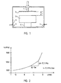
- a resonator comprises inductive coupling loops 5 (input and output), a dielectric resonator disc 3 installed in a metal casing 4 and supported by a dielectric leg 6, and a frequency controller attached to the metal casing 4, comprising an adjustment screw 1 and a metal plate 2.
- the resonance frequency of the resonator depends on the distance L between the resonator disc 3 and the metal plate 2 in accordance with a graph in Figure 2.
- frequency adjustment is based on a highly accurate mechanical movement, the slope of adjustment k also being steep.
- the resonance frequency becomes higher, e.g. to the range 1500-2000 MHz or higher, the dimensions of the basic elements of the dielectric filter, such as those of the resonator disc 3 or the adjustment mechanism 1,2 are reduced.
- adjusting the resonance frequency of a dielectric resonator with prior art solutions sets very high demands on the frequency adjustment mechanism, which, in turn, increases the material and production costs.
- adjustment will be slower.
- the object of the invention is a dielectric resonator providing a higher adjustment accuracy and speed.
- the resonator of the invention consists of a pair of joined adjustment plates, such as metal plates, which are mechanically engaged with each other so that their movement with respect to each other and the ceramic body provides two adjustment phases during one adjusting movement.
- the smaller adjustment plate moves a predetermined distance with respect to the larger adjustment plate and the dielectric body, while the larger adjustment plate remains stationary by means of a specific friction surface. Once the smaller adjustment plate has moved said distance, the larger adjustment plate also starts to move in accordance with the adjusting movement.
- the frequency controller of the resonator having two slopes of adjustment, whereby the adjustment is fast owing to the movement of both adjustment plates, and also extremely accurate owing to the fine adjustment function, which is achieved when the smaller adjustment plate is moved alone.
- the adjustment accuracy may be improved as much as tenfold, so that the demands on the accuracy of the adjustment mechanics do not have to be made stricter when the frequency is increased, or they may be even moderated for the presently used frequencies.
- dielectric resonators The structure, the operation and the ceramic manufacturing materials of dielectric resonators are disclosed e.g. in the above-mentioned articles [1] , [2] , and [3]. In the following description, only the parts in the structure of the dielectric resonator which are essential to the invention will be disclosed.
- dielectric resonator body generally refers to any object which has a suitable geometric shape, and the manufacturing material of which exhibits low dielectric losses and a high relative dielectric constant.
- a dielectric resonator is usually of a cylindrical shape, such as a cylindrical disc.
- the most commonly used material is ceramic material.
- Figure 3 shows a dielectric resonator of the invention, comprising a dielectric, preferably cylindrical resonator disc 35 inside a casing 36 made of an electrically conductive material, such as metal, said disc being preferably ceramic and installed at a fixed distance from the bottom of the casing 36, on a supporting leg 38 of a suitable dielectric or isolating material.
- the casing 36 is coupled to the ground potential.
- the resonance frequency adjustment mechanism comprises adjustment plates 33 and 34 of metal (or some other electrically conductive material), an adjustment mechanism 31, and a bushing 42, as well as cylindrical supporting blocks 32 and 40, of isolating material.
- FIG. 3 shows by way of example coupling to the resonator by inductive coupling loops 37, which provide the input and the output of the resonator.
- the resonator frequency of a dielectric resonator is primarily determined by the dimensions of the dielectric body 35. Another factor that has an effect on the resonance frequency is the environment of the dielectric body 35.
- adjustment plates 33 and 34 function as a conductive surface.
- the adjustment plate consists of two combined adjustment planes 33 and 34, which are mechanically engaged with each other so that their movement with respect to each other and with respect to the ceramic body provides two adjustment phases during one adjusting movement.
- the smaller adjustment plate 34 moves with respect to the larger adjustment plate 33 and the planar top surface of the dielectric body 35 a predetermined distance L2, while the larger adjustment plate remains stationary by means of a specific friction surface. Once the smaller adjustment plate has moved said distance L2, the larger adjustment plate 33 also starts to move in accordance with the adjusting movement.
- the frequency adjustment mechanism comprises a cylindrical supporting block 40, one end of which is connected to a casing 36. Inside supporting block 40 there is a second cylindrical supporting block 32 gliding telescopically on its inner surface.
- the inner surface of supporting block 40 and/or the outer surface of supporting block 32 is a friction surface so that a predetermined friction acts against the movement of supporting block 32.
- a ring-shaped adjustment plate made of metal or some other electrically conductive material is connected to the lower end of the cylindrical supporting block 32.
- the second adjustment plate 34 is connected to the lower end of an adjustment screw 31, and arranged to be located in the centre hole of the ring-shaped adjustment plate 33 and to be connected to supporting block 32 in a manner which transfers the movement of the adjustment screw 31 so that it first moves adjustment plate 34 with respect to the planar surface of the resonator disc 35 for a predetermined adjustment range L2, and thereafter both the ring-shaped adjustment plate 33 and adjustment plate 34.
- Adjustment plate 34 which is preferably a bent ring-shaped metal film, is connected by its edges to a shoulder 41, and in the middle to the lower end of the adjustment screw 31.
- the adjustment screw 31 is connected by threads to a bushing 42 so that by turning the adjustment screw 31, it is possible to adjust the length of the screw 31 in an air-filled inside 39 of the casing 36, and thus the distance of adjustment plates 33 and 34 from the planar top surface of the resonator disc 35.
- the axial movement of the adjustment screw 31 first causes bending of the metal film 34, until bending reaches its maximum value, whereafter the movement of the adjustment screw 31 is transferred via the metal film 34, also into the movement of the ring-shaped adjustment plate 33.
- a dielectric resonator is achieved the frequency controller of which has two slopes of adjustment, whereby the adjustment is fast when both adjustment plates 33 and 34 are moved, and slower, but extremely accurate when the smaller adjustment plate 34 is moved alone.
- the graph of Figure 4 shows the resonance frequency fo of the resonator of the invention as a function of the movement L of the adjustment plate.
- curve A describes the adjustment when both adjustment plates are moved, the slope of adjustment k being e.g. 5.5 MHz/mm.
- fine adjustment is performed solely with a movement of adjustment plate 34, which is achieved by changing the rotating direction of the adjustment screw 31.
Landscapes
- Control Of Motors That Do Not Use Commutators (AREA)
Claims (4)
- Dielektrischer Resonator miteinem dielektrischen Körper (35) mit zumindest einer ebenen Oberfläche,einer Frequenzsteuerung mit einem Einstellungsmechanismus (31) und einer elektrisch leitenden Einstellungsplatte (33), die zu der ebenen Oberfläche des dielektrischen Körpers (35) im wesentlichen parallel und zur Einstellung der Resonanzfrequenz mittels des Einstellungsmechanismus (31) in senkrechter Richtung bezüglich der Resonatorscheiben beweglich ist, indem der Abstand zwischen der Einstellungsplatte und der ebenen Oberfläche des dielektrischen Körpers verändert wird, undeinem elektrisch leitenden Gehäuse (36) dadurch gekennzeichnet, daß die Frequenzsteuerung zudem versehen ist miteinem ersten zylindrischen Unterstützungsblock (40), der mit dem Gehäuse (36) verbunden ist, und einem zweiten zylindrischen Unterstützungsblock (32), der innerhalb des ersten Blockes an Reibungsoberflächen entlang ausziehbar gleitet,einer ringförmigen elektrisch leitenden Einstellungsplatte (33), die mit dem zweiten zylindrischen Unterstützungsblock verbunden ist,einer zweiten elektrisch leitenden Einstellungsplatte (34), die mit dem Einstellungsmechanismus (31) verbunden, in dem Zentralloch der ringförmigen Einstellungsplatte (33) angeordnet und mit dem zweiten Unterstützungsblock (32) in einer Art verbunden ist, daß die Bewegung des Einstellungsmechanismus (31) so übertragen wird, daß zunächst die zweite Einstellungsplatte (34) bezüglich der ebenen Oberfläche des Keramikkörpers für einen vorbestimmten Einstellungsbereich bewegt wird, und danach sowohl die ringförmige Einstellungsplatte (33) als auch die zweite Einstellungsplatte (34) bewegt wird.
- Dielektrischer Resonator nach Anspruch 1,
dadurch gekennzeichnet, daß
die zweite Einstellungsplatte eine konvex gebogene ringförmige Metallschicht (34) ist, die an ihren Kanten mit dem zweiten Unterstützungsblock (32) und in der Mitte mit einem Ende des Einstellungsmechanismus (31) verbunden ist, wodurch eine Bewegung des Einstellungsmechanismus zunächst eine Verbiegung der Metallschicht (34) verursacht, bis die Verbiegung ihren maximalen Wert erreicht, wonach die Bewegung des Einstellungsmechanismus (31) über die Metallschicht (34) auch in die Bewegung der ringförmigen Einstellungsplatte (33) übertragen wird. - Dielektrischer Resonator nach Anspruch 1 oder 2,
dadurch gekennzeichnet, daß
während der Bewegung der ringförmigen Einstellungsplatte (33) die Frequenzeinstellung einen ersten Abfall der Einstellung aufweist, und während der Bewegung der zweiten Einstellungsplatte (34) alleine die Frequenzeinstellung einen zweiten Abfall der Einstellung aufweist, wobei der zweite Abfall der Einstellung verglichen mit dem ersten Abfall der Einstellung bedeutend geringer ist. - Dielektrischer Resonator nach einem beliebigen der vorstehenden Ansprüche,
dadurch gekennzeichnet, daß
der Einstellungsmechanismus eine Einstellungsschraube (31) aufweist.
Applications Claiming Priority (3)
| Application Number | Priority Date | Filing Date | Title |
|---|---|---|---|
| FI944663 | 1994-10-05 | ||
| FI944663A FI97090C (fi) | 1994-10-05 | 1994-10-05 | Dielektrinen resonaattori |
| PCT/FI1995/000547 WO1996011511A1 (en) | 1994-10-05 | 1995-10-04 | Dielectric resonator |
Publications (2)
| Publication Number | Publication Date |
|---|---|
| EP0731989A1 EP0731989A1 (de) | 1996-09-18 |
| EP0731989B1 true EP0731989B1 (de) | 2000-01-26 |
Family
ID=8541513
Family Applications (1)
| Application Number | Title | Priority Date | Filing Date |
|---|---|---|---|
| EP95934145A Expired - Lifetime EP0731989B1 (de) | 1994-10-05 | 1995-10-04 | Dielektrischer resonator |
Country Status (9)
| Country | Link |
|---|---|
| US (1) | US5677653A (de) |
| EP (1) | EP0731989B1 (de) |
| JP (1) | JP3181057B2 (de) |
| CN (1) | CN1136368A (de) |
| AT (1) | ATE189346T1 (de) |
| DE (1) | DE69514781T2 (de) |
| FI (1) | FI97090C (de) |
| NO (1) | NO962312L (de) |
| WO (1) | WO1996011511A1 (de) |
Families Citing this family (7)
| Publication number | Priority date | Publication date | Assignee | Title |
|---|---|---|---|---|
| DE19841078C1 (de) * | 1998-09-09 | 2000-05-18 | Forschungszentrum Juelich Gmbh | Abstimmbarer Hohlraumresonator |
| US6791430B2 (en) | 2001-12-31 | 2004-09-14 | Conductus, Inc. | Resonator tuning assembly and method |
| KR100769657B1 (ko) * | 2003-08-23 | 2007-10-23 | 주식회사 케이엠더블유 | 무선 주파수 대역 가변 필터 |
| US7610072B2 (en) * | 2003-09-18 | 2009-10-27 | Superconductor Technologies, Inc. | Superconductive stripline filter utilizing one or more inter-resonator coupling members |
| US7193489B2 (en) * | 2004-12-03 | 2007-03-20 | Motorola, Inc. | Radio frequency cavity resonator with heat transport apparatus |
| US7148771B2 (en) * | 2004-12-21 | 2006-12-12 | Alcatel | Concentric, two stage coarse and fine tuning for ceramic resonators |
| FI127061B (en) * | 2014-05-23 | 2017-10-31 | Tongyu Tech Oy | Control element for radio frequency resonator |
Family Cites Families (4)
| Publication number | Priority date | Publication date | Assignee | Title |
|---|---|---|---|---|
| JPS5127757A (de) * | 1974-09-02 | 1976-03-08 | Hitachi Ltd | |
| US4565979A (en) * | 1984-12-10 | 1986-01-21 | Ford Aerospace & Communications Corporation | Double dielectric resonator stabilized oscillator |
| IT1248509B (it) * | 1991-06-19 | 1995-01-19 | Sits Soc It Telecom Siemens | Cavita' risonante a microonde a doppio risonatore dielettrico con frequenza di risonanza sintonizzabile. |
| JP3117914U (ja) | 2005-10-24 | 2006-01-19 | 靖子 久保 | フラワーアレンジメント装置 |
-
1994
- 1994-10-05 FI FI944663A patent/FI97090C/fi active IP Right Grant
-
1995
- 1995-10-04 EP EP95934145A patent/EP0731989B1/de not_active Expired - Lifetime
- 1995-10-04 WO PCT/FI1995/000547 patent/WO1996011511A1/en not_active Ceased
- 1995-10-04 US US08/640,795 patent/US5677653A/en not_active Expired - Lifetime
- 1995-10-04 AT AT95934145T patent/ATE189346T1/de not_active IP Right Cessation
- 1995-10-04 DE DE69514781T patent/DE69514781T2/de not_active Expired - Fee Related
- 1995-10-04 JP JP51235696A patent/JP3181057B2/ja not_active Expired - Fee Related
- 1995-10-04 CN CN95190989.4A patent/CN1136368A/zh active Pending
-
1996
- 1996-06-04 NO NO962312A patent/NO962312L/no not_active Application Discontinuation
Also Published As
| Publication number | Publication date |
|---|---|
| CN1136368A (zh) | 1996-11-20 |
| JPH09506495A (ja) | 1997-06-24 |
| DE69514781D1 (de) | 2000-03-02 |
| NO962312D0 (no) | 1996-06-04 |
| ATE189346T1 (de) | 2000-02-15 |
| EP0731989A1 (de) | 1996-09-18 |
| FI944663A0 (fi) | 1994-10-05 |
| FI944663A7 (fi) | 1996-04-06 |
| FI97090C (fi) | 1996-10-10 |
| NO962312L (no) | 1996-06-04 |
| WO1996011511A1 (en) | 1996-04-18 |
| US5677653A (en) | 1997-10-14 |
| FI97090B (fi) | 1996-06-28 |
| AU3654495A (en) | 1996-05-02 |
| AU687260B2 (en) | 1998-02-19 |
| DE69514781T2 (de) | 2000-06-15 |
| JP3181057B2 (ja) | 2001-07-03 |
Similar Documents
| Publication | Publication Date | Title |
|---|---|---|
| EP0731990B1 (de) | Dielektrischer resonator | |
| EP0748526B1 (de) | Dielektrischer resonator | |
| EP0731989B1 (de) | Dielektrischer resonator | |
| EP0748525B1 (de) | Dielektrischer resonator | |
| JP3137338B2 (ja) | 誘電体共振器構造 | |
| EP0538429B1 (de) | Dielektrischer resonator | |
| EP0731988B1 (de) | Dielektrischer resonator | |
| AU687260C (en) | Dielectric resonator | |
| AU686892C (en) | Dielectric resonator | |
| AU687259C (en) | Dielectric resonator | |
| AU686887C (en) | Dielectric resonator |
Legal Events
| Date | Code | Title | Description |
|---|---|---|---|
| PUAI | Public reference made under article 153(3) epc to a published international application that has entered the european phase |
Free format text: ORIGINAL CODE: 0009012 |
|
| 17P | Request for examination filed |
Effective date: 19960511 |
|
| AK | Designated contracting states |
Kind code of ref document: A1 Designated state(s): AT BE CH DE DK ES FR GB GR IE IT LI LU MC NL PT SE |
|
| RAP1 | Party data changed (applicant data changed or rights of an application transferred) |
Owner name: NOKIA TELECOMMUNICATIONS OY |
|
| GRAG | Despatch of communication of intention to grant |
Free format text: ORIGINAL CODE: EPIDOS AGRA |
|
| 17Q | First examination report despatched |
Effective date: 19990525 |
|
| GRAG | Despatch of communication of intention to grant |
Free format text: ORIGINAL CODE: EPIDOS AGRA |
|
| GRAH | Despatch of communication of intention to grant a patent |
Free format text: ORIGINAL CODE: EPIDOS IGRA |
|
| GRAH | Despatch of communication of intention to grant a patent |
Free format text: ORIGINAL CODE: EPIDOS IGRA |
|
| GRAA | (expected) grant |
Free format text: ORIGINAL CODE: 0009210 |
|
| RAP1 | Party data changed (applicant data changed or rights of an application transferred) |
Owner name: NOKIA NETWORKS OY |
|
| AK | Designated contracting states |
Kind code of ref document: B1 Designated state(s): AT BE CH DE DK ES FR GB GR IE IT LI LU MC NL PT SE |
|
| PG25 | Lapsed in a contracting state [announced via postgrant information from national office to epo] |
Ref country code: GR Free format text: LAPSE BECAUSE OF NON-PAYMENT OF DUE FEES Effective date: 20000126 Ref country code: ES Free format text: THE PATENT HAS BEEN ANNULLED BY A DECISION OF A NATIONAL AUTHORITY Effective date: 20000126 |
|
| REF | Corresponds to: |
Ref document number: 189346 Country of ref document: AT Date of ref document: 20000215 Kind code of ref document: T |
|
| REG | Reference to a national code |
Ref country code: CH Ref legal event code: NV Representative=s name: ICB INGENIEURS CONSEILS EN BREVETS SA Ref country code: CH Ref legal event code: EP |
|
| REF | Corresponds to: |
Ref document number: 69514781 Country of ref document: DE Date of ref document: 20000302 |
|
| ET | Fr: translation filed | ||
| REG | Reference to a national code |
Ref country code: IE Ref legal event code: FG4D |
|
| ITF | It: translation for a ep patent filed | ||
| PG25 | Lapsed in a contracting state [announced via postgrant information from national office to epo] |
Ref country code: PT Free format text: LAPSE BECAUSE OF FAILURE TO SUBMIT A TRANSLATION OF THE DESCRIPTION OR TO PAY THE FEE WITHIN THE PRESCRIBED TIME-LIMIT Effective date: 20000426 Ref country code: DK Free format text: LAPSE BECAUSE OF FAILURE TO SUBMIT A TRANSLATION OF THE DESCRIPTION OR TO PAY THE FEE WITHIN THE PRESCRIBED TIME-LIMIT Effective date: 20000426 |
|
| PG25 | Lapsed in a contracting state [announced via postgrant information from national office to epo] |
Ref country code: LU Free format text: LAPSE BECAUSE OF NON-PAYMENT OF DUE FEES Effective date: 20001004 Ref country code: IE Free format text: LAPSE BECAUSE OF NON-PAYMENT OF DUE FEES Effective date: 20001004 |
|
| PG25 | Lapsed in a contracting state [announced via postgrant information from national office to epo] |
Ref country code: MC Free format text: THE PATENT HAS BEEN ANNULLED BY A DECISION OF A NATIONAL AUTHORITY Effective date: 20001031 |
|
| PLBE | No opposition filed within time limit |
Free format text: ORIGINAL CODE: 0009261 |
|
| STAA | Information on the status of an ep patent application or granted ep patent |
Free format text: STATUS: NO OPPOSITION FILED WITHIN TIME LIMIT |
|
| 26N | No opposition filed | ||
| REG | Reference to a national code |
Ref country code: IE Ref legal event code: MM4A |
|
| PGFP | Annual fee paid to national office [announced via postgrant information from national office to epo] |
Ref country code: SE Payment date: 20011005 Year of fee payment: 7 |
|
| PGFP | Annual fee paid to national office [announced via postgrant information from national office to epo] |
Ref country code: AT Payment date: 20011011 Year of fee payment: 7 |
|
| PGFP | Annual fee paid to national office [announced via postgrant information from national office to epo] |
Ref country code: CH Payment date: 20011015 Year of fee payment: 7 |
|
| PGFP | Annual fee paid to national office [announced via postgrant information from national office to epo] |
Ref country code: NL Payment date: 20011031 Year of fee payment: 7 |
|
| PGFP | Annual fee paid to national office [announced via postgrant information from national office to epo] |
Ref country code: BE Payment date: 20011129 Year of fee payment: 7 |
|
| REG | Reference to a national code |
Ref country code: GB Ref legal event code: IF02 |
|
| PG25 | Lapsed in a contracting state [announced via postgrant information from national office to epo] |
Ref country code: AT Free format text: LAPSE BECAUSE OF NON-PAYMENT OF DUE FEES Effective date: 20021004 |
|
| PG25 | Lapsed in a contracting state [announced via postgrant information from national office to epo] |
Ref country code: SE Free format text: LAPSE BECAUSE OF NON-PAYMENT OF DUE FEES Effective date: 20021005 |
|
| PG25 | Lapsed in a contracting state [announced via postgrant information from national office to epo] |
Ref country code: LI Free format text: LAPSE BECAUSE OF NON-PAYMENT OF DUE FEES Effective date: 20021031 Ref country code: CH Free format text: LAPSE BECAUSE OF NON-PAYMENT OF DUE FEES Effective date: 20021031 Ref country code: BE Free format text: LAPSE BECAUSE OF NON-PAYMENT OF DUE FEES Effective date: 20021031 |
|
| BERE | Be: lapsed |
Owner name: *NOKIA NETWORKS OY Effective date: 20021031 |
|
| PG25 | Lapsed in a contracting state [announced via postgrant information from national office to epo] |
Ref country code: NL Free format text: LAPSE BECAUSE OF NON-PAYMENT OF DUE FEES Effective date: 20030501 |
|
| EUG | Se: european patent has lapsed | ||
| REG | Reference to a national code |
Ref country code: CH Ref legal event code: PL |
|
| NLV4 | Nl: lapsed or anulled due to non-payment of the annual fee |
Effective date: 20030501 |
|
| PGFP | Annual fee paid to national office [announced via postgrant information from national office to epo] |
Ref country code: DE Payment date: 20040930 Year of fee payment: 10 |
|
| PGFP | Annual fee paid to national office [announced via postgrant information from national office to epo] |
Ref country code: FR Payment date: 20041008 Year of fee payment: 10 |
|
| PGFP | Annual fee paid to national office [announced via postgrant information from national office to epo] |
Ref country code: GB Payment date: 20050928 Year of fee payment: 11 |
|
| PG25 | Lapsed in a contracting state [announced via postgrant information from national office to epo] |
Ref country code: IT Free format text: LAPSE BECAUSE OF NON-PAYMENT OF DUE FEES;WARNING: LAPSES OF ITALIAN PATENTS WITH EFFECTIVE DATE BEFORE 2007 MAY HAVE OCCURRED AT ANY TIME BEFORE 2007. THE CORRECT EFFECTIVE DATE MAY BE DIFFERENT FROM THE ONE RECORDED. Effective date: 20051004 |
|
| PG25 | Lapsed in a contracting state [announced via postgrant information from national office to epo] |
Ref country code: DE Free format text: LAPSE BECAUSE OF NON-PAYMENT OF DUE FEES Effective date: 20060503 |
|
| PG25 | Lapsed in a contracting state [announced via postgrant information from national office to epo] |
Ref country code: FR Free format text: LAPSE BECAUSE OF NON-PAYMENT OF DUE FEES Effective date: 20060630 |
|
| REG | Reference to a national code |
Ref country code: FR Ref legal event code: ST Effective date: 20060630 |
|
| GBPC | Gb: european patent ceased through non-payment of renewal fee |
Effective date: 20061004 |
|
| PG25 | Lapsed in a contracting state [announced via postgrant information from national office to epo] |
Ref country code: GB Free format text: LAPSE BECAUSE OF NON-PAYMENT OF DUE FEES Effective date: 20061004 |