EP0731982B1 - A method of treating a semiconductor wafer - Google Patents
A method of treating a semiconductor wafer Download PDFInfo
- Publication number
- EP0731982B1 EP0731982B1 EP93914846A EP93914846A EP0731982B1 EP 0731982 B1 EP0731982 B1 EP 0731982B1 EP 93914846 A EP93914846 A EP 93914846A EP 93914846 A EP93914846 A EP 93914846A EP 0731982 B1 EP0731982 B1 EP 0731982B1
- Authority
- EP
- European Patent Office
- Prior art keywords
- layer
- wafer
- compound
- vapour
- silicon
- Prior art date
- Legal status (The legal status is an assumption and is not a legal conclusion. Google has not performed a legal analysis and makes no representation as to the accuracy of the status listed.)
- Expired - Lifetime
Links
- 239000004065 semiconductor Substances 0.000 title claims abstract description 9
- 238000000034 method Methods 0.000 title claims description 45
- MHAJPDPJQMAIIY-UHFFFAOYSA-N Hydrogen peroxide Chemical compound OO MHAJPDPJQMAIIY-UHFFFAOYSA-N 0.000 claims abstract description 34
- 229920000642 polymer Polymers 0.000 claims abstract description 28
- 239000007789 gas Substances 0.000 claims abstract description 22
- XUIMIQQOPSSXEZ-UHFFFAOYSA-N Silicon Chemical compound [Si] XUIMIQQOPSSXEZ-UHFFFAOYSA-N 0.000 claims abstract description 15
- 229910052710 silicon Inorganic materials 0.000 claims abstract description 15
- 239000010703 silicon Substances 0.000 claims abstract description 15
- 238000010438 heat treatment Methods 0.000 claims description 16
- 150000001875 compounds Chemical class 0.000 claims description 14
- 238000000151 deposition Methods 0.000 claims description 13
- BLRPTPMANUNPDV-UHFFFAOYSA-N Silane Chemical group [SiH4] BLRPTPMANUNPDV-UHFFFAOYSA-N 0.000 claims description 12
- XLYOFNOQVPJJNP-UHFFFAOYSA-N water Substances O XLYOFNOQVPJJNP-UHFFFAOYSA-N 0.000 claims description 12
- VYPSYNLAJGMNEJ-UHFFFAOYSA-N Silicium dioxide Chemical group O=[Si]=O VYPSYNLAJGMNEJ-UHFFFAOYSA-N 0.000 claims description 10
- 230000008021 deposition Effects 0.000 claims description 7
- 229910000077 silane Inorganic materials 0.000 claims description 5
- 239000000377 silicon dioxide Substances 0.000 claims description 5
- 238000005229 chemical vapour deposition Methods 0.000 claims description 4
- 239000007788 liquid Substances 0.000 claims description 4
- 238000006243 chemical reaction Methods 0.000 claims description 3
- LYCAIKOWRPUZTN-UHFFFAOYSA-N Ethylene glycol Chemical compound OCCO LYCAIKOWRPUZTN-UHFFFAOYSA-N 0.000 claims description 2
- 229910052681 coesite Inorganic materials 0.000 claims 1
- 229910052906 cristobalite Inorganic materials 0.000 claims 1
- 230000001419 dependent effect Effects 0.000 claims 1
- 229910052682 stishovite Inorganic materials 0.000 claims 1
- 229910052905 tridymite Inorganic materials 0.000 claims 1
- 239000012530 fluid Substances 0.000 abstract 1
- 235000012431 wafers Nutrition 0.000 description 20
- IJGRMHOSHXDMSA-UHFFFAOYSA-N Atomic nitrogen Chemical compound N#N IJGRMHOSHXDMSA-UHFFFAOYSA-N 0.000 description 5
- 238000004132 cross linking Methods 0.000 description 5
- 235000012239 silicon dioxide Nutrition 0.000 description 4
- QVGXLLKOCUKJST-UHFFFAOYSA-N atomic oxygen Chemical compound [O] QVGXLLKOCUKJST-UHFFFAOYSA-N 0.000 description 3
- 239000004020 conductor Substances 0.000 description 3
- 229910052757 nitrogen Inorganic materials 0.000 description 3
- 239000001301 oxygen Substances 0.000 description 3
- 229910052760 oxygen Inorganic materials 0.000 description 3
- 230000005855 radiation Effects 0.000 description 3
- 239000012159 carrier gas Substances 0.000 description 2
- 239000000356 contaminant Substances 0.000 description 2
- 238000005336 cracking Methods 0.000 description 2
- 239000011810 insulating material Substances 0.000 description 2
- 239000000758 substrate Substances 0.000 description 2
- MYMOFIZGZYHOMD-UHFFFAOYSA-N Dioxygen Chemical compound O=O MYMOFIZGZYHOMD-UHFFFAOYSA-N 0.000 description 1
- MWUXSHHQAYIFBG-UHFFFAOYSA-N Nitrogen oxide Substances O=[N] MWUXSHHQAYIFBG-UHFFFAOYSA-N 0.000 description 1
- 239000004642 Polyimide Substances 0.000 description 1
- 230000001133 acceleration Effects 0.000 description 1
- 239000006227 byproduct Substances 0.000 description 1
- 238000006482 condensation reaction Methods 0.000 description 1
- 238000010276 construction Methods 0.000 description 1
- 238000001816 cooling Methods 0.000 description 1
- 229910001882 dioxygen Inorganic materials 0.000 description 1
- 238000009826 distribution Methods 0.000 description 1
- 230000000694 effects Effects 0.000 description 1
- 239000001257 hydrogen Substances 0.000 description 1
- 229910052739 hydrogen Inorganic materials 0.000 description 1
- 125000004435 hydrogen atom Chemical class [H]* 0.000 description 1
- 239000011261 inert gas Substances 0.000 description 1
- 229920000592 inorganic polymer Polymers 0.000 description 1
- 238000010849 ion bombardment Methods 0.000 description 1
- 239000000463 material Substances 0.000 description 1
- 229960003753 nitric oxide Drugs 0.000 description 1
- 239000002245 particle Substances 0.000 description 1
- 150000002978 peroxides Chemical class 0.000 description 1
- 238000005334 plasma enhanced chemical vapour deposition Methods 0.000 description 1
- 238000009832 plasma treatment Methods 0.000 description 1
- 238000000623 plasma-assisted chemical vapour deposition Methods 0.000 description 1
- 229920001721 polyimide Polymers 0.000 description 1
- 230000000191 radiation effect Effects 0.000 description 1
- 150000004756 silanes Chemical class 0.000 description 1
- 239000007858 starting material Substances 0.000 description 1
Images


Classifications
-
- H—ELECTRICITY
- H01—ELECTRIC ELEMENTS
- H01L—SEMICONDUCTOR DEVICES NOT COVERED BY CLASS H10
- H01L21/00—Processes or apparatus adapted for the manufacture or treatment of semiconductor or solid state devices or of parts thereof
- H01L21/67—Apparatus specially adapted for handling semiconductor or electric solid state devices during manufacture or treatment thereof; Apparatus specially adapted for handling wafers during manufacture or treatment of semiconductor or electric solid state devices or components ; Apparatus not specifically provided for elsewhere
- H01L21/67005—Apparatus not specifically provided for elsewhere
- H01L21/67011—Apparatus for manufacture or treatment
- H01L21/67017—Apparatus for fluid treatment
-
- B—PERFORMING OPERATIONS; TRANSPORTING
- B05—SPRAYING OR ATOMISING IN GENERAL; APPLYING FLUENT MATERIALS TO SURFACES, IN GENERAL
- B05D—PROCESSES FOR APPLYING FLUENT MATERIALS TO SURFACES, IN GENERAL
- B05D1/00—Processes for applying liquids or other fluent materials
- B05D1/60—Deposition of organic layers from vapour phase
-
- H—ELECTRICITY
- H01—ELECTRIC ELEMENTS
- H01L—SEMICONDUCTOR DEVICES NOT COVERED BY CLASS H10
- H01L21/00—Processes or apparatus adapted for the manufacture or treatment of semiconductor or solid state devices or of parts thereof
- H01L21/02—Manufacture or treatment of semiconductor devices or of parts thereof
- H01L21/02104—Forming layers
- H01L21/02107—Forming insulating materials on a substrate
- H01L21/02109—Forming insulating materials on a substrate characterised by the type of layer, e.g. type of material, porous/non-porous, pre-cursors, mixtures or laminates
- H01L21/02112—Forming insulating materials on a substrate characterised by the type of layer, e.g. type of material, porous/non-porous, pre-cursors, mixtures or laminates characterised by the material of the layer
- H01L21/02123—Forming insulating materials on a substrate characterised by the type of layer, e.g. type of material, porous/non-porous, pre-cursors, mixtures or laminates characterised by the material of the layer the material containing silicon
- H01L21/02164—Forming insulating materials on a substrate characterised by the type of layer, e.g. type of material, porous/non-porous, pre-cursors, mixtures or laminates characterised by the material of the layer the material containing silicon the material being a silicon oxide, e.g. SiO2
-
- H—ELECTRICITY
- H01—ELECTRIC ELEMENTS
- H01L—SEMICONDUCTOR DEVICES NOT COVERED BY CLASS H10
- H01L21/00—Processes or apparatus adapted for the manufacture or treatment of semiconductor or solid state devices or of parts thereof
- H01L21/02—Manufacture or treatment of semiconductor devices or of parts thereof
- H01L21/02104—Forming layers
- H01L21/02107—Forming insulating materials on a substrate
- H01L21/02109—Forming insulating materials on a substrate characterised by the type of layer, e.g. type of material, porous/non-porous, pre-cursors, mixtures or laminates
- H01L21/02205—Forming insulating materials on a substrate characterised by the type of layer, e.g. type of material, porous/non-porous, pre-cursors, mixtures or laminates the layer being characterised by the precursor material for deposition
- H01L21/02208—Forming insulating materials on a substrate characterised by the type of layer, e.g. type of material, porous/non-porous, pre-cursors, mixtures or laminates the layer being characterised by the precursor material for deposition the precursor containing a compound comprising Si
- H01L21/02211—Forming insulating materials on a substrate characterised by the type of layer, e.g. type of material, porous/non-porous, pre-cursors, mixtures or laminates the layer being characterised by the precursor material for deposition the precursor containing a compound comprising Si the compound being a silane, e.g. disilane, methylsilane or chlorosilane
-
- H—ELECTRICITY
- H01—ELECTRIC ELEMENTS
- H01L—SEMICONDUCTOR DEVICES NOT COVERED BY CLASS H10
- H01L21/00—Processes or apparatus adapted for the manufacture or treatment of semiconductor or solid state devices or of parts thereof
- H01L21/02—Manufacture or treatment of semiconductor devices or of parts thereof
- H01L21/02104—Forming layers
- H01L21/02107—Forming insulating materials on a substrate
- H01L21/02225—Forming insulating materials on a substrate characterised by the process for the formation of the insulating layer
- H01L21/0226—Forming insulating materials on a substrate characterised by the process for the formation of the insulating layer formation by a deposition process
- H01L21/02263—Forming insulating materials on a substrate characterised by the process for the formation of the insulating layer formation by a deposition process deposition from the gas or vapour phase
- H01L21/02271—Forming insulating materials on a substrate characterised by the process for the formation of the insulating layer formation by a deposition process deposition from the gas or vapour phase deposition by decomposition or reaction of gaseous or vapour phase compounds, i.e. chemical vapour deposition
-
- H—ELECTRICITY
- H01—ELECTRIC ELEMENTS
- H01L—SEMICONDUCTOR DEVICES NOT COVERED BY CLASS H10
- H01L21/00—Processes or apparatus adapted for the manufacture or treatment of semiconductor or solid state devices or of parts thereof
- H01L21/02—Manufacture or treatment of semiconductor devices or of parts thereof
- H01L21/02104—Forming layers
- H01L21/02107—Forming insulating materials on a substrate
- H01L21/02296—Forming insulating materials on a substrate characterised by the treatment performed before or after the formation of the layer
- H01L21/02299—Forming insulating materials on a substrate characterised by the treatment performed before or after the formation of the layer pre-treatment
- H01L21/02304—Forming insulating materials on a substrate characterised by the treatment performed before or after the formation of the layer pre-treatment formation of intermediate layers, e.g. buffer layers, layers to improve adhesion, lattice match or diffusion barriers
-
- H—ELECTRICITY
- H01—ELECTRIC ELEMENTS
- H01L—SEMICONDUCTOR DEVICES NOT COVERED BY CLASS H10
- H01L21/00—Processes or apparatus adapted for the manufacture or treatment of semiconductor or solid state devices or of parts thereof
- H01L21/02—Manufacture or treatment of semiconductor devices or of parts thereof
- H01L21/02104—Forming layers
- H01L21/02107—Forming insulating materials on a substrate
- H01L21/02296—Forming insulating materials on a substrate characterised by the treatment performed before or after the formation of the layer
- H01L21/02318—Forming insulating materials on a substrate characterised by the treatment performed before or after the formation of the layer post-treatment
- H01L21/02345—Forming insulating materials on a substrate characterised by the treatment performed before or after the formation of the layer post-treatment treatment by exposure to radiation, e.g. visible light
- H01L21/02348—Forming insulating materials on a substrate characterised by the treatment performed before or after the formation of the layer post-treatment treatment by exposure to radiation, e.g. visible light treatment by exposure to UV light
-
- H—ELECTRICITY
- H01—ELECTRIC ELEMENTS
- H01L—SEMICONDUCTOR DEVICES NOT COVERED BY CLASS H10
- H01L21/00—Processes or apparatus adapted for the manufacture or treatment of semiconductor or solid state devices or of parts thereof
- H01L21/02—Manufacture or treatment of semiconductor devices or of parts thereof
- H01L21/02104—Forming layers
- H01L21/02107—Forming insulating materials on a substrate
- H01L21/02296—Forming insulating materials on a substrate characterised by the treatment performed before or after the formation of the layer
- H01L21/02318—Forming insulating materials on a substrate characterised by the treatment performed before or after the formation of the layer post-treatment
- H01L21/02362—Forming insulating materials on a substrate characterised by the treatment performed before or after the formation of the layer post-treatment formation of intermediate layers, e.g. capping layers or diffusion barriers
-
- H—ELECTRICITY
- H01—ELECTRIC ELEMENTS
- H01L—SEMICONDUCTOR DEVICES NOT COVERED BY CLASS H10
- H01L21/00—Processes or apparatus adapted for the manufacture or treatment of semiconductor or solid state devices or of parts thereof
- H01L21/02—Manufacture or treatment of semiconductor devices or of parts thereof
- H01L21/04—Manufacture or treatment of semiconductor devices or of parts thereof the devices having potential barriers, e.g. a PN junction, depletion layer or carrier concentration layer
- H01L21/18—Manufacture or treatment of semiconductor devices or of parts thereof the devices having potential barriers, e.g. a PN junction, depletion layer or carrier concentration layer the devices having semiconductor bodies comprising elements of Group IV of the Periodic Table or AIIIBV compounds with or without impurities, e.g. doping materials
- H01L21/30—Treatment of semiconductor bodies using processes or apparatus not provided for in groups H01L21/20 - H01L21/26
- H01L21/31—Treatment of semiconductor bodies using processes or apparatus not provided for in groups H01L21/20 - H01L21/26 to form insulating layers thereon, e.g. for masking or by using photolithographic techniques; After treatment of these layers; Selection of materials for these layers
- H01L21/312—Organic layers, e.g. photoresist
- H01L21/3121—Layers comprising organo-silicon compounds
-
- H—ELECTRICITY
- H01—ELECTRIC ELEMENTS
- H01L—SEMICONDUCTOR DEVICES NOT COVERED BY CLASS H10
- H01L21/00—Processes or apparatus adapted for the manufacture or treatment of semiconductor or solid state devices or of parts thereof
- H01L21/02—Manufacture or treatment of semiconductor devices or of parts thereof
- H01L21/04—Manufacture or treatment of semiconductor devices or of parts thereof the devices having potential barriers, e.g. a PN junction, depletion layer or carrier concentration layer
- H01L21/18—Manufacture or treatment of semiconductor devices or of parts thereof the devices having potential barriers, e.g. a PN junction, depletion layer or carrier concentration layer the devices having semiconductor bodies comprising elements of Group IV of the Periodic Table or AIIIBV compounds with or without impurities, e.g. doping materials
- H01L21/30—Treatment of semiconductor bodies using processes or apparatus not provided for in groups H01L21/20 - H01L21/26
- H01L21/31—Treatment of semiconductor bodies using processes or apparatus not provided for in groups H01L21/20 - H01L21/26 to form insulating layers thereon, e.g. for masking or by using photolithographic techniques; After treatment of these layers; Selection of materials for these layers
- H01L21/314—Inorganic layers
- H01L21/316—Inorganic layers composed of oxides or glassy oxides or oxide based glass
- H01L21/31604—Deposition from a gas or vapour
- H01L21/31608—Deposition of SiO2
- H01L21/31612—Deposition of SiO2 on a silicon body
-
- H—ELECTRICITY
- H01—ELECTRIC ELEMENTS
- H01L—SEMICONDUCTOR DEVICES NOT COVERED BY CLASS H10
- H01L21/00—Processes or apparatus adapted for the manufacture or treatment of semiconductor or solid state devices or of parts thereof
- H01L21/02—Manufacture or treatment of semiconductor devices or of parts thereof
- H01L21/02104—Forming layers
- H01L21/02107—Forming insulating materials on a substrate
- H01L21/02109—Forming insulating materials on a substrate characterised by the type of layer, e.g. type of material, porous/non-porous, pre-cursors, mixtures or laminates
- H01L21/02112—Forming insulating materials on a substrate characterised by the type of layer, e.g. type of material, porous/non-porous, pre-cursors, mixtures or laminates characterised by the material of the layer
- H01L21/02123—Forming insulating materials on a substrate characterised by the type of layer, e.g. type of material, porous/non-porous, pre-cursors, mixtures or laminates characterised by the material of the layer the material containing silicon
- H01L21/02126—Forming insulating materials on a substrate characterised by the type of layer, e.g. type of material, porous/non-porous, pre-cursors, mixtures or laminates characterised by the material of the layer the material containing silicon the material containing Si, O, and at least one of H, N, C, F, or other non-metal elements, e.g. SiOC, SiOC:H or SiONC
-
- H—ELECTRICITY
- H01—ELECTRIC ELEMENTS
- H01L—SEMICONDUCTOR DEVICES NOT COVERED BY CLASS H10
- H01L21/00—Processes or apparatus adapted for the manufacture or treatment of semiconductor or solid state devices or of parts thereof
- H01L21/02—Manufacture or treatment of semiconductor devices or of parts thereof
- H01L21/02104—Forming layers
- H01L21/02107—Forming insulating materials on a substrate
- H01L21/02109—Forming insulating materials on a substrate characterised by the type of layer, e.g. type of material, porous/non-porous, pre-cursors, mixtures or laminates
- H01L21/02112—Forming insulating materials on a substrate characterised by the type of layer, e.g. type of material, porous/non-porous, pre-cursors, mixtures or laminates characterised by the material of the layer
- H01L21/02123—Forming insulating materials on a substrate characterised by the type of layer, e.g. type of material, porous/non-porous, pre-cursors, mixtures or laminates characterised by the material of the layer the material containing silicon
- H01L21/02167—Forming insulating materials on a substrate characterised by the type of layer, e.g. type of material, porous/non-porous, pre-cursors, mixtures or laminates characterised by the material of the layer the material containing silicon the material being a silicon carbide not containing oxygen, e.g. SiC, SiC:H or silicon carbonitrides
-
- H—ELECTRICITY
- H01—ELECTRIC ELEMENTS
- H01L—SEMICONDUCTOR DEVICES NOT COVERED BY CLASS H10
- H01L21/00—Processes or apparatus adapted for the manufacture or treatment of semiconductor or solid state devices or of parts thereof
- H01L21/02—Manufacture or treatment of semiconductor devices or of parts thereof
- H01L21/02104—Forming layers
- H01L21/02107—Forming insulating materials on a substrate
- H01L21/02109—Forming insulating materials on a substrate characterised by the type of layer, e.g. type of material, porous/non-porous, pre-cursors, mixtures or laminates
- H01L21/02205—Forming insulating materials on a substrate characterised by the type of layer, e.g. type of material, porous/non-porous, pre-cursors, mixtures or laminates the layer being characterised by the precursor material for deposition
- H01L21/02208—Forming insulating materials on a substrate characterised by the type of layer, e.g. type of material, porous/non-porous, pre-cursors, mixtures or laminates the layer being characterised by the precursor material for deposition the precursor containing a compound comprising Si
- H01L21/02214—Forming insulating materials on a substrate characterised by the type of layer, e.g. type of material, porous/non-porous, pre-cursors, mixtures or laminates the layer being characterised by the precursor material for deposition the precursor containing a compound comprising Si the compound comprising silicon and oxygen
- H01L21/02216—Forming insulating materials on a substrate characterised by the type of layer, e.g. type of material, porous/non-porous, pre-cursors, mixtures or laminates the layer being characterised by the precursor material for deposition the precursor containing a compound comprising Si the compound comprising silicon and oxygen the compound being a molecule comprising at least one silicon-oxygen bond and the compound having hydrogen or an organic group attached to the silicon or oxygen, e.g. a siloxane
-
- Y—GENERAL TAGGING OF NEW TECHNOLOGICAL DEVELOPMENTS; GENERAL TAGGING OF CROSS-SECTIONAL TECHNOLOGIES SPANNING OVER SEVERAL SECTIONS OF THE IPC; TECHNICAL SUBJECTS COVERED BY FORMER USPC CROSS-REFERENCE ART COLLECTIONS [XRACs] AND DIGESTS
- Y10—TECHNICAL SUBJECTS COVERED BY FORMER USPC
- Y10S—TECHNICAL SUBJECTS COVERED BY FORMER USPC CROSS-REFERENCE ART COLLECTIONS [XRACs] AND DIGESTS
- Y10S438/00—Semiconductor device manufacturing: process
- Y10S438/935—Gas flow control
Definitions
- This invention relates to a method for treating a semi-conductor wafer and in particular, but not exclusively, to what is known as planarisation.
- US-A-4812325 describes a method of depositing a film using silanes and peroxides as starting materials to form a film on a substrate.
- the resultant films suffered from distribution irregularity of film thickness.
- the invention consists in a method of treating a semiconductor wafer, including positioning the wafer on a platen in a chamber, introducing into the chamber silicon-containing gas or vapour and a compound, containing peroxide bonding, in vapour form, maintaining the platen at or below the dew point of the silicon containing gas, reacting the silicon-containing gas or vapour with the compound to form, as a condensate, a liquid short-chain polymer on the wafer to form a generally planar layer.
- the silicon containing gas and the compound may be reacted in a chemical vapour deposition process.
- the reaction may take place between electrodes in which case the silicon-containing gas and the compound are kept apart until they are introduced between the electrodes.
- the silicon-containing gas or vapour may be inorganic and preferably is silane or a higher silane, which may be introduced into the chamber with an inert carrier gas, for example nitrogen.
- the compound may be, for example, hydrogen peroxide or ethandiol.
- the hydrogen peroxide may be between 45% and 55% concentration and is preferably 50% concentration.
- the method may further comprise removing water and/or OH from the layer.
- the layer may be exposed to a reduced pressure (conveniently for between 1.5 and 2.5 minutes) and/or exposed to a low power density plasma, which may heat the layer to 40° to 120°C.
- the method may further comprise forming or depositing an under layer prior to the deposition of the polymer.
- the underlayer may be deposited using chemical vapour deposition and the wafer may be preheated prior to the underlayer deposition.
- This under layer may be silicon dioxide and may have a thickness of between 1000 and 3000 ⁇ . It may for example be 2000 ⁇ thick.
- the under layer may conveniently be deposited by plasma enhanced chemically vapour deposition.
- Either the under layer and/or the wafer may be pre-treated by, for example a plasma, to removing contaminants. In that case it may be pretreated with a plasma, for example using oxygen as a reactive gas.
- the surface of the deposited polymer layer may be treated in a plasma using a reactive oxygen gas in order to enhance chain lengthening and cross-linking within the polymer.
- This gas could be, for example, oxygen, nitrogen or hydrogen peroxide vapour and other gases may be appropriate.
- the plasma has a heating effect which enhances crosslinking, but there may also be a radiation effect from the various gases.
- This chain linking may alternatively be catalysed by exposing the polymer layer to UV light, x-rays or ion bombardment. However, in many applications acceleration of chain linking may not be desirable; instead it may be desirable for the polymer molecule particles to settle before significant chain linking occurs.
- the method may further comprise depositing or forming a capping layer on the surface of the deposited layer.
- This capping layer may be silicon dioxide.
- the capping layer is deposited after a proportion of the condensation reactions have occured and substantially all of the water has been removed from the polymer layer.
- the method may further comprise heating the polymer layer and this heating preferably takes place after capping.
- the polymer layer may be heated to between 180-220°C for between 50-70 minutes. For example it may be heated to 220°C for 60 minutes.
- the layer may subsequently be allowed to cool to an ambient temperature and then reheated to 430-470°C for 30-50 minutes.
- the second heating may last 40 minutes at 450°C. Indeed this second heating may suffice and may be achieved using a furnace, heat lamps, a hotplate or plasma heating.
- the polymer layer may be heated to between 200-450°C, prior to capping, in order that the cap can be deposited at elevated temperatures.
- the capping layer could be deposited in one or more steps e.g. a 'cold' capping layer deposited at the temperature of the planarising layer followed by a hot capping layer; the polymer layer having first been heated to 200-450°C as described above.
- the density of the hydrogen peroxide may be in the range of 1.20-1.35 gms/cc and a density of 1.25 gms/cc may be particularly preferred.
- the hydrogen peroxide is preferably at 50% concentration when introduced into the chamber.
- the ambient temperature within the chamber may be within the range of 0-80°C during the deposition of the polymer layer, but the wafer platen is preferably at 0°C or at the dew point of the polymer when in vapour form.
- Low pressure is also desirable but requires low temperatures (eg 400mT, -10°C).
- the wafer is preferably lifted from the platen for each processing step which involves heating.
- the lifted position may be between the platen and a wafer load/unload position.
- the method can be used to achieve planarisation or gap filling.
- the ambient chamber temperature may conveniently be even higher.
- the invention also includes wafers treated by any of the methods set out above and semi-conductor devices including polymer layers formed by the method above.
- Apparatus for treating semi-conductor wafers is schematically illustrated at 10 in Figure 1. It will be understood that only the features which are particularly required for the understanding of the invention are described and illustrated. The general construction of such apparatus is well known in the art.
- the apparatus 10 includes a chamber 11 having a duplex shower head 12 and a wafer support or platen 13.
- the shower head 12 is connected to RF source 14 to form one electrode, whilst the support 13 is earthed and forms another electrode.
- the R.F. source 14 could be connected to the support 13 and the shower head 12 earthed.
- the shower head 12 is connected by respective pipes 15 and 16 to a source of SiH 4 in N 2 or other inert carrier and a source 16 of H 2 O 2 .
- the carrier gas is conveniently used for ease of operation of the equipment; it is believed that the process could be performed without it.
- the source 16 comprises a reservoir 17 of H 2 O 2 , an outlet pipe 18, a pump 19 and a flash heater 20 for vaporising the H 2 O 2 .
- the apparatus is arranged to deposit a short chain, inorganic polymer, which is initially a liquid, between the interconnects on a semi-conductor chip to produce planarisation either locally or globally, or for 'gap filling'.
- the polymer is formed by introducing into the chamber the silane and the hydrogen peroxide in vapour form and reacting them within the chamber spontaneously.
- the resultant polymer is deposited on the wafer, it has been found that its viscosity is such that it fills both small and large geometries or gaps and is generally self levelling. It is believed that effectively there is a settlement process taking place as the polymerisation takes place. The more settlement which occurs prior to full polymerisation the less likelihood there is of cracking. Very small dimensioned gaps can be filled and because of the fill layer properties these gaps can even, in certain circumstances, be re-entrant.
- a suitable capping layer would be silicon dioxide.
- the heat treatment stage after the capping involves removing excess water from the layer which is a by-product of the cross-linking reaction.
- the bake also removes SioH bonds.
- the speed at which the water is removed may be important and several ways of removing water have been successful.
- One suitable sequence comprises baking the layer for 60 minutes at 200°C, cooling it to ambient temperature and then rebaking it for 40 minutes at 450°C. Microwave heating has also been successful.
- a simple bake at 450° will often also suffice, or the bakes may be replaced by the following steps:
- adhesion of the polymer layer to the underlying substrate material can be enhanced by depositing an under layer, for example of silicon dioxide. Typically this should be of the order of 2000 ⁇ thickness and it may be laid down by plasma-enhanced chemical vapour deposition.
- SiH 4 has proved to be particularly successful, it is believed that the method will be applicable with most silicon-containing gases or vapours. It has been found that to some extent a suitable polymer can be obtained with any concentration or density of H 2 O 2 , but a density range 1.20-1.35 gms/cc has been particularly successful. The most preferred H 2 O 2 density is 1.25 gms/cc. An H 2 O 2 concentration of 50% is very effective but it is believed that the preferred concentration may vary depending on whether the object is to achieve planarisation or gap filling. It is preferred that more H 2 O 2 is supplied than SiH 4 and it is particulary preferred that the H 2 O 2 :SiH 4 ratio is of the order of 3:1.
- the wafer In the event that the wafer needs to be removed from the chamber between processing stages, it may be desirable to pre-treat the exposed surface, when the wafer is placed back in the chamber, in order to remove any organics or other contaminants from the exposed surface.
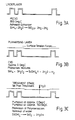
- Figures 3A to E illustrate the preferred processing sequence schematically and indicate the probable chemistry. It may be advantageous to wash the chamber with H 2 O 2 , of other compound containg peroxide bonding that is being used between at least some of the processing stages.
- the wafer may be lifted above the support 13 for each heating process so that the heat of the wafer is not significantly transmitted to the support 13. This can be achieved by arranging an intermediate position 23 for a wafer loading device 21.
Landscapes
- Engineering & Computer Science (AREA)
- Condensed Matter Physics & Semiconductors (AREA)
- General Physics & Mathematics (AREA)
- Manufacturing & Machinery (AREA)
- Computer Hardware Design (AREA)
- Microelectronics & Electronic Packaging (AREA)
- Power Engineering (AREA)
- Physics & Mathematics (AREA)
- Chemical & Material Sciences (AREA)
- Chemical Kinetics & Catalysis (AREA)
- Formation Of Insulating Films (AREA)
- Mechanical Treatment Of Semiconductor (AREA)
- Treatments Of Macromolecular Shaped Articles (AREA)
- Internal Circuitry In Semiconductor Integrated Circuit Devices (AREA)
- Crystals, And After-Treatments Of Crystals (AREA)
- Physical Vapour Deposition (AREA)
- Weting (AREA)
- Element Separation (AREA)
- Polymerisation Methods In General (AREA)
- Cleaning Or Drying Semiconductors (AREA)
Abstract
Description
- This invention relates to a method for treating a semi-conductor wafer and in particular, but not exclusively, to what is known as planarisation.
- It is common practice in the semi-conductor industry to lay down layers of insulating material between conducting layers in order to prevent short circuits. If a layer of insulating material is simply deposited in the normal way undulations begin to build up as the layers pass over the metallic conductors which they are designed to insulate. Various techniques have been developed to try to overcome this problem by filling the trenches or valleys between the conductors to a height above the top of the conductors so that after treatment a generally planar layer exists on the top of the wafer. One example of such a technique is to spin on layers of polyimide to smooth out the surfaces. However, in practice, narrow trenches tend to be incompletely filled whilst wide valleys are not fully levelled. As the 2-D dimensions of devices are reduced, these problems are accentuated.
- US-A-4812325 describes a method of depositing a film using silanes and peroxides as starting materials to form a film on a substrate. The resultant films suffered from distribution irregularity of film thickness.
- References in the specification to the polymer being liquid are simply intended to indicate that it is neither gaseous nor solidified at the moment of deposition.
- From one aspect the invention consists in a method of treating a semiconductor wafer, including positioning the wafer on a platen in a chamber, introducing into the chamber silicon-containing gas or vapour and a compound, containing peroxide bonding, in vapour form, maintaining the platen at or below the dew point of the silicon containing gas, reacting the silicon-containing gas or vapour with the compound to form, as a condensate, a liquid short-chain polymer on the wafer to form a generally planar layer.
- The silicon containing gas and the compound may be reacted in a chemical vapour deposition process. The reaction may take place between electrodes in which case the silicon-containing gas and the compound are kept apart until they are introduced between the electrodes.
- The silicon-containing gas or vapour may be inorganic and preferably is silane or a higher silane, which may be introduced into the chamber with an inert carrier gas, for example nitrogen. The compound may be, for example, hydrogen peroxide or ethandiol. The hydrogen peroxide may be between 45% and 55% concentration and is preferably 50% concentration.
- The method may further comprise removing water and/or OH from the layer. For example the layer may be exposed to a reduced pressure (conveniently for between 1.5 and 2.5 minutes) and/or exposed to a low power density plasma, which may heat the layer to 40° to 120°C.
- The method may further comprise forming or depositing an under layer prior to the deposition of the polymer. The underlayer may be deposited using chemical vapour deposition and the wafer may be preheated prior to the underlayer deposition. This under layer may be silicon dioxide and may have a thickness of between 1000 and 3000Å. It may for example be 2000Å thick. The under layer may conveniently be deposited by plasma enhanced chemically vapour deposition. Either the under layer and/or the wafer may be pre-treated by, for example a plasma, to removing contaminants. In that case it may be pretreated with a plasma, for example using oxygen as a reactive gas.
- Similarly the surface of the deposited polymer layer may be treated in a plasma using a reactive oxygen gas in order to enhance chain lengthening and cross-linking within the polymer. This gas could be, for example, oxygen, nitrogen or hydrogen peroxide vapour and other gases may be appropriate. The plasma has a heating effect which enhances crosslinking, but there may also be a radiation effect from the various gases. This chain linking may alternatively be catalysed by exposing the polymer layer to UV light, x-rays or ion bombardment. However, in many applications acceleration of chain linking may not be desirable; instead it may be desirable for the polymer molecule particles to settle before significant chain linking occurs.
- The method may further comprise depositing or forming a capping layer on the surface of the deposited layer. This capping layer may be silicon dioxide. The capping layer is deposited after a proportion of the condensation reactions have occured and substantially all of the water has been removed from the polymer layer.
- The method may further comprise heating the polymer layer and this heating preferably takes place after capping. The polymer layer may be heated to between 180-220°C for between 50-70 minutes. For example it may be heated to 220°C for 60 minutes. The layer may subsequently be allowed to cool to an ambient temperature and then reheated to 430-470°C for 30-50 minutes. For example the second heating may last 40 minutes at 450°C. Indeed this second heating may suffice and may be achieved using a furnace, heat lamps, a hotplate or plasma heating.
- In one preferred arrangement the polymer layer may be heated to between 200-450°C, prior to capping, in order that the cap can be deposited at elevated temperatures. Although the capping layer could be deposited in one or more steps e.g. a 'cold' capping layer deposited at the temperature of the planarising layer followed by a hot capping layer; the polymer layer having first been heated to 200-450°C as described above.
- The density of the hydrogen peroxide may be in the range of 1.20-1.35 gms/cc and a density of 1.25 gms/cc may be particularly preferred. The hydrogen peroxide is preferably at 50% concentration when introduced into the chamber.
- The ambient temperature within the chamber may be within the range of 0-80°C during the deposition of the polymer layer, but the wafer platen is preferably at 0°C or at the dew point of the polymer when in vapour form. Low pressure is also desirable but requires low temperatures (eg 400mT, -10°C).
- In order to avoid heating the platen, the wafer is preferably lifted from the platen for each processing step which involves heating. The lifted position may be between the platen and a wafer load/unload position.
- The method can be used to achieve planarisation or gap filling. In the latter case the ambient chamber temperature may conveniently be even higher.
- The invention also includes wafers treated by any of the methods set out above and semi-conductor devices including polymer layers formed by the method above.
- The invention may be performed in various ways and a specific embodiment will now be described, by way of example, with reference to the following drawings, in which;
- Figure 1 is a schematic view for apparatus for performing the treatment method;
- Figures 2A and 2B are hugely magnified photographs of cross-sections of a wafer treated by the method; and
- Figures 3A to E illustrate schematically the steps of the process.
-
- Apparatus for treating semi-conductor wafers is schematically illustrated at 10 in Figure 1. It will be understood that only the features which are particularly required for the understanding of the invention are described and illustrated. The general construction of such apparatus is well known in the art.
- Thus, the
apparatus 10 includes achamber 11 having aduplex shower head 12 and a wafer support or platen 13. Theshower head 12 is connected toRF source 14 to form one electrode, whilst the support 13 is earthed and forms another electrode. Alternatively the R.F.source 14 could be connected to the support 13 and theshower head 12 earthed. Theshower head 12 is connected byrespective pipes source 16 of H2O2. The carrier gas is conveniently used for ease of operation of the equipment; it is believed that the process could be performed without it. - The
source 16 comprises areservoir 17 of H2O2, anoutlet pipe 18, apump 19 and aflash heater 20 for vaporising the H2O2. - In use the apparatus is arranged to deposit a short chain, inorganic polymer, which is initially a liquid, between the interconnects on a semi-conductor chip to produce planarisation either locally or globally, or for 'gap filling'. The polymer is formed by introducing into the chamber the silane and the hydrogen peroxide in vapour form and reacting them within the chamber spontaneously. Once the resultant polymer is deposited on the wafer, it has been found that its viscosity is such that it fills both small and large geometries or gaps and is generally self levelling. It is believed that effectively there is a settlement process taking place as the polymerisation takes place. The more settlement which occurs prior to full polymerisation the less likelihood there is of cracking. Very small dimensioned gaps can be filled and because of the fill layer properties these gaps can even, in certain circumstances, be re-entrant.
- As has been mentioned, if left, the chains within the polymer will slowly extend and cross link. In some circumstances it may be desirable to accelerate this process by plasma treatment. This treatment produces UV radiation and it is believed that it is this radiation which is responsible for increasing the speed of chain extension and cross linking. Other forms of radiation treatment may therefore be equally applicable. A variety of gases may be appropriate for use at this stage, for example any inert gas or hydrogen, nitrogen or oxygen containing gases.
- For good quality films it is desirable to remove as much water and OH from the film at an early stage. This can be done by exposing the layer to a reduced pressure causing the layer to pump water out and the subsequently heating the layer to between say 40°C and 120°
C. A pump 22 is provided for reducing chamber pressure. - However in order to solidify fully the polymer layer, it has been found that it is generally necessary to subject the layer to more intense heat treatment. In many instances it is necessary or desirable first to deposit a capping layer over the polymer. It is believed that this assists in providing mechanical stability for the polymer layer during cross linking. It may also help to control the rate at which the layer looses water during heating and so have a controlling affect on shrinkage and cracking.
- A suitable capping layer would be silicon dioxide.
- The heat treatment stage after the capping involves removing excess water from the layer which is a by-product of the cross-linking reaction. The bake also removes SioH bonds. The speed at which the water is removed may be important and several ways of removing water have been successful. One suitable sequence comprises baking the layer for 60 minutes at 200°C, cooling it to ambient temperature and then rebaking it for 40 minutes at 450°C. Microwave heating has also been successful. A simple bake at 450° will often also suffice, or the bakes may be replaced by the following steps:
- 1. 2000 Å 'cold' cap deposited at between 20-40°C.
- 2. Plasma heat treatment in N2O which raises the temperature to 300-400°C.
- 3. 4000-6000Å 'hot' cap is deposited.
-
- Alternatively, in some cases, a single stage 'hot cap' deposited at 300-400°C will suffice.
- It has been found that the adhesion of the polymer layer to the underlying substrate material can be enhanced by depositing an under layer, for example of silicon dioxide. Typically this should be of the order of 2000Å thickness and it may be laid down by plasma-enhanced chemical vapour deposition.
- Examples of actual deposited layers are illustrated in the photographs of Figures 2A and 2B. It will be seen that the upper surface of the
layers 21 are generally planar despite the huge magnification involved. - Although SiH4 has proved to be particularly successful, it is believed that the method will be applicable with most silicon-containing gases or vapours. It has been found that to some extent a suitable polymer can be obtained with any concentration or density of H2O2, but a density range 1.20-1.35 gms/cc has been particularly successful. The most preferred H2O2 density is 1.25 gms/cc. An H2O2 concentration of 50% is very effective but it is believed that the preferred concentration may vary depending on whether the object is to achieve planarisation or gap filling. It is preferred that more H2O2 is supplied than SiH4 and it is particulary preferred that the H2O2:SiH4 ratio is of the order of 3:1.
- In the event that the wafer needs to be removed from the chamber between processing stages, it may be desirable to pre-treat the exposed surface, when the wafer is placed back in the chamber, in order to remove any organics or other contaminants from the exposed surface.
- Figures 3A to E illustrate the preferred processing sequence schematically and indicate the probable chemistry. It may be advantageous to wash the chamber with H2O2, of other compound containg peroxide bonding that is being used between at least some of the processing stages.
- As it is desirable to keep the platen or support 13 at around 0°C, the wafer may be lifted above the support 13 for each heating process so that the heat of the wafer is not significantly transmitted to the support 13. This can be achieved by arranging an
intermediate position 23 for awafer loading device 21.
Claims (23)
- A method of treating a semi-conductor wafer, including positioning the wafer on a platen in a chamber, introducing into the chamber silicon-containing gas or vapour and a compound, containing peroxide bonding, in vapour form, maintaining the platen at or below the dew point of the silicon containing gas, reacting the silicon-containing gas or vapour with the compound to form, as a condensate, a liquid short-chain polymer on the wafer to form a generally planar layer.
- A method as claimed in Claim 2, wherein the silicon-containing gas or vapour is a silane or higher silane.
- A method as claimed in Claim 1 or Claim 2, wherein the compound is hydrogen peroxide or ethandiol.
- A method as claimed in any one of the preceding claims further comprising removing water and/or OH from the layer.
- A method as claimed in Claim 4, wherein the water and/or OH removing step includes exposing the layer to a reduced pressure.
- A method as claimed in Claim 5, wherein the layer is exposed to reduced pressure for between 1.5 and 2.5 minutes.
- A method as claimed in any one of the Claims 4 to 6, wherein water and/or OH removing step includes exposing the layer to a low power density plasma.
- A method as claimed in Claim 7, wherein the plasma heats the layer to between 40° to 120°C.
- A method as claimed in any one of the preceding claims further comprising forming or depositing an under layer prior to the deposition of the polymer layer.
- A method as claimed in Claim 9, wherein the under layer is deposited by chemical vapour deposition.
- A method as claimed in Claim 10, wherein the wafer is preheated prior to the under layer deposition.
- A method as claimed in any one of the preceding claims further comprising depositing a capping layer on the polymer layer after substantially all the water has been removed from the polymer layer.
- A method as claimed in Claim 12, wherein the capping layer is SiO2.
- A method as claimed in Claim 12 or Claim 13, including heat treating the wafer after the capping layer has been deposited.
- A method as claimed in any one of the preceding Claims, wherein the wafer is lifted from the platen for any processing step involving or causing heating of the wafer.
- A method as claimed in Claim 15, wherein the lifted position lies between the platen and a wafer load/unload position.
- A method as claimed in Claim 3 and Claims 4 to 16 as dependent on Claim 4 wherein the compound is hydrogen peroxide of between 45% and 55% concentration.
- A method as claimed in Claim 17, wherein the concentration of the hydrogen peroxide is 50%.
- A method as claimed in any one of Claims 1 to 18, wherein the silicon-containing gas or vapour and the compound are reacted in a chemical vapour deposition process.
- A method as claimed in Claim 19, wherein the reaction takes place between electrodes and wherein the silicon-containing gas or vapour and the compound are kept apart until they are introduced between the electrodes.
- A method as claimed in any one of the preceding Claims wherein the gas is SiH4 and the compound is H2O2 and there is more H2O2 than SiH4.
- A method as claimed in Claim 21, wherein the H2O2:SiH4 ratio is of the order of 3:1.
- A method as claimed in any one of the preceding Claims wherein the chamber is washed through with the compound between at least two processing steps.
Applications Claiming Priority (7)
| Application Number | Priority Date | Filing Date | Title |
|---|---|---|---|
| GB929214243A GB9214243D0 (en) | 1992-07-04 | 1992-07-04 | A method of treating a semi-conductor wafer |
| GB9214243 | 1992-07-04 | ||
| GB929221519A GB9221519D0 (en) | 1992-10-14 | 1992-10-14 | A method of treating a semi-conductor wafer |
| GB9221520 | 1992-10-14 | ||
| GB9221519 | 1992-10-14 | ||
| GB929221520A GB9221520D0 (en) | 1992-10-14 | 1992-10-14 | A method of treating a semiconductor wafer |
| PCT/GB1993/001368 WO1994001885A1 (en) | 1992-07-04 | 1993-06-30 | A method of treating a semiconductor wafer |
Publications (2)
| Publication Number | Publication Date |
|---|---|
| EP0731982A1 EP0731982A1 (en) | 1996-09-18 |
| EP0731982B1 true EP0731982B1 (en) | 1999-12-01 |
Family
ID=27266279
Family Applications (1)
| Application Number | Title | Priority Date | Filing Date |
|---|---|---|---|
| EP93914846A Expired - Lifetime EP0731982B1 (en) | 1992-07-04 | 1993-06-30 | A method of treating a semiconductor wafer |
Country Status (11)
| Country | Link |
|---|---|
| US (2) | US5874367A (en) |
| EP (1) | EP0731982B1 (en) |
| JP (1) | JP3262334B2 (en) |
| KR (1) | KR100286192B1 (en) |
| CN (1) | CN1042577C (en) |
| AT (1) | ATE187277T1 (en) |
| AU (1) | AU4506993A (en) |
| CA (1) | CA2137928C (en) |
| DE (1) | DE69327176T2 (en) |
| TW (1) | TW253974B (en) |
| WO (1) | WO1994001885A1 (en) |
Families Citing this family (130)
| Publication number | Priority date | Publication date | Assignee | Title |
|---|---|---|---|---|
| JP3262334B2 (en) | 1992-07-04 | 2002-03-04 | トリコン ホルディングズ リミテッド | Method for processing semiconductor wafers |
| US5858880A (en) * | 1994-05-14 | 1999-01-12 | Trikon Equipment Limited | Method of treating a semi-conductor wafer |
| GB9409713D0 (en) * | 1994-05-14 | 1994-07-06 | Electrotech Equipments Ltd | A method of treating a semi-conductor wafer |
| JPH08181276A (en) * | 1994-12-26 | 1996-07-12 | Toshiba Corp | Manufacture of semiconductor device |
| KR100345663B1 (en) * | 1995-04-11 | 2002-10-30 | 주식회사 하이닉스반도체 | A method for inter-dielectric planarization of film in semiconductor device |
| FR2734402B1 (en) * | 1995-05-15 | 1997-07-18 | Brouquet Pierre | PROCESS FOR ELECTRICAL ISOLATION IN MICROELECTRONICS, APPLICABLE TO NARROW CAVITIES, BY DEPOSITION OF OXIDE IN THE VISCOUS STATE AND CORRESPONDING DEVICE |
| GB9515449D0 (en) * | 1995-07-27 | 1995-09-27 | Electrotech Equipments Ltd | Monitoring apparatus and methods |
| JPH0951035A (en) * | 1995-08-07 | 1997-02-18 | Mitsubishi Electric Corp | Formation of interlayer insulation layer |
| JPH0992717A (en) * | 1995-09-21 | 1997-04-04 | Mitsubishi Electric Corp | Semiconductor and fabrication thereof |
| JPH09205087A (en) * | 1996-01-26 | 1997-08-05 | Sony Corp | Deposition of insulation film |
| US6114186A (en) * | 1996-07-30 | 2000-09-05 | Texas Instruments Incorporated | Hydrogen silsesquioxane thin films for low capacitance structures in integrated circuits |
| GB2331626B (en) * | 1996-08-24 | 2001-06-13 | Trikon Equip Ltd | Method and apparatus for depositing a planarized dielectric layer on a semiconductor substrate |
| JPH1126449A (en) * | 1997-06-30 | 1999-01-29 | Sony Corp | Formation of insulating film |
| US6455394B1 (en) * | 1998-03-13 | 2002-09-24 | Micron Technology, Inc. | Method for trench isolation by selective deposition of low temperature oxide films |
| GB9801359D0 (en) * | 1998-01-23 | 1998-03-18 | Poulton Limited | Methods and apparatus for treating a substrate |
| GB9801655D0 (en) * | 1998-01-28 | 1998-03-25 | Trikon Equip Ltd | Method and apparatus for treating a substrate |
| US6593247B1 (en) | 1998-02-11 | 2003-07-15 | Applied Materials, Inc. | Method of depositing low k films using an oxidizing plasma |
| US6303523B2 (en) | 1998-02-11 | 2001-10-16 | Applied Materials, Inc. | Plasma processes for depositing low dielectric constant films |
| US6287990B1 (en) | 1998-02-11 | 2001-09-11 | Applied Materials, Inc. | CVD plasma assisted low dielectric constant films |
| US6627532B1 (en) * | 1998-02-11 | 2003-09-30 | Applied Materials, Inc. | Method of decreasing the K value in SiOC layer deposited by chemical vapor deposition |
| US6340435B1 (en) | 1998-02-11 | 2002-01-22 | Applied Materials, Inc. | Integrated low K dielectrics and etch stops |
| US6413583B1 (en) | 1998-02-11 | 2002-07-02 | Applied Materials, Inc. | Formation of a liquid-like silica layer by reaction of an organosilicon compound and a hydroxyl forming compound |
| US6660656B2 (en) | 1998-02-11 | 2003-12-09 | Applied Materials Inc. | Plasma processes for depositing low dielectric constant films |
| US6054379A (en) * | 1998-02-11 | 2000-04-25 | Applied Materials, Inc. | Method of depositing a low k dielectric with organo silane |
| US7804115B2 (en) * | 1998-02-25 | 2010-09-28 | Micron Technology, Inc. | Semiconductor constructions having antireflective portions |
| US6274292B1 (en) * | 1998-02-25 | 2001-08-14 | Micron Technology, Inc. | Semiconductor processing methods |
| US6068884A (en) * | 1998-04-28 | 2000-05-30 | Silcon Valley Group Thermal Systems, Llc | Method of making low κ dielectric inorganic/organic hybrid films |
| GB9810917D0 (en) * | 1998-05-21 | 1998-07-22 | Trikon Technologies Ltd | Method and apparatus for treating a semi-conductor substrate |
| US7923383B2 (en) | 1998-05-21 | 2011-04-12 | Tokyo Electron Limited | Method and apparatus for treating a semi-conductor substrate |
| US6159871A (en) * | 1998-05-29 | 2000-12-12 | Dow Corning Corporation | Method for producing hydrogenated silicon oxycarbide films having low dielectric constant |
| US6667553B2 (en) | 1998-05-29 | 2003-12-23 | Dow Corning Corporation | H:SiOC coated substrates |
| US6268282B1 (en) | 1998-09-03 | 2001-07-31 | Micron Technology, Inc. | Semiconductor processing methods of forming and utilizing antireflective material layers, and methods of forming transistor gate stacks |
| US6383951B1 (en) | 1998-09-03 | 2002-05-07 | Micron Technology, Inc. | Low dielectric constant material for integrated circuit fabrication |
| US6281100B1 (en) | 1998-09-03 | 2001-08-28 | Micron Technology, Inc. | Semiconductor processing methods |
| US6136703A (en) * | 1998-09-03 | 2000-10-24 | Micron Technology, Inc. | Methods for forming phosphorus- and/or boron-containing silica layers on substrates |
| US6323101B1 (en) * | 1998-09-03 | 2001-11-27 | Micron Technology, Inc. | Semiconductor processing methods, methods of forming silicon dioxide methods of forming trench isolation regions, and methods of forming interlevel dielectric layers |
| US6800571B2 (en) * | 1998-09-29 | 2004-10-05 | Applied Materials Inc. | CVD plasma assisted low dielectric constant films |
| US6171945B1 (en) | 1998-10-22 | 2001-01-09 | Applied Materials, Inc. | CVD nanoporous silica low dielectric constant films |
| US6372301B1 (en) * | 1998-12-22 | 2002-04-16 | Applied Materials, Inc. | Method of improving adhesion of diffusion layers on fluorinated silicon dioxide |
| US6828683B2 (en) | 1998-12-23 | 2004-12-07 | Micron Technology, Inc. | Semiconductor devices, and semiconductor processing methods |
| US7235499B1 (en) | 1999-01-20 | 2007-06-26 | Micron Technology, Inc. | Semiconductor processing methods |
| JP2002538604A (en) | 1999-02-26 | 2002-11-12 | トリコン ホールディングス リミティド | Processing method of polymer layer |
| GB2355992B (en) | 1999-06-26 | 2004-06-02 | Trikon Holdings Ltd | Method and apparatus for forming a film on a substrate |
| KR100735876B1 (en) | 1999-07-30 | 2007-07-06 | 동경 엘렉트론 주식회사 | Substrate processing method and substrate processing apparatus |
| US7067414B1 (en) | 1999-09-01 | 2006-06-27 | Micron Technology, Inc. | Low k interlevel dielectric layer fabrication methods |
| US6395647B1 (en) * | 1999-09-02 | 2002-05-28 | Micron Technology, Inc. | Chemical treatment of semiconductor substrates |
| US6156743A (en) * | 1999-10-18 | 2000-12-05 | Whitcomb; John E. | Method of decreasing fatigue |
| US6756674B1 (en) | 1999-10-22 | 2004-06-29 | Lsi Logic Corporation | Low dielectric constant silicon oxide-based dielectric layer for integrated circuit structures having improved compatibility with via filler materials, and method of making same |
| US6423628B1 (en) | 1999-10-22 | 2002-07-23 | Lsi Logic Corporation | Method of forming integrated circuit structure having low dielectric constant material and having silicon oxynitride caps over closely spaced apart metal lines |
| US6391795B1 (en) | 1999-10-22 | 2002-05-21 | Lsi Logic Corporation | Low k dielectric composite layer for intergrated circuit structure which provides void-free low k dielectric material between metal lines while mitigating via poisoning |
| US6316354B1 (en) | 1999-10-26 | 2001-11-13 | Lsi Logic Corporation | Process for removing resist mask of integrated circuit structure which mitigates damage to underlying low dielectric constant silicon oxide dielectric layer |
| US6399489B1 (en) | 1999-11-01 | 2002-06-04 | Applied Materials, Inc. | Barrier layer deposition using HDP-CVD |
| US6147012A (en) * | 1999-11-12 | 2000-11-14 | Lsi Logic Corporation | Process for forming low k silicon oxide dielectric material while suppressing pressure spiking and inhibiting increase in dielectric constant |
| US6759337B1 (en) | 1999-12-15 | 2004-07-06 | Lsi Logic Corporation | Process for etching a controllable thickness of oxide on an integrated circuit structure on a semiconductor substrate using nitrogen plasma and plasma and an rf bias applied to the substrate |
| US6440860B1 (en) | 2000-01-18 | 2002-08-27 | Micron Technology, Inc. | Semiconductor processing methods of transferring patterns from patterned photoresists to materials, and structures comprising silicon nitride |
| US6346490B1 (en) | 2000-04-05 | 2002-02-12 | Lsi Logic Corporation | Process for treating damaged surfaces of low k carbon doped silicon oxide dielectric material after plasma etching and plasma cleaning steps |
| US6426286B1 (en) | 2000-05-19 | 2002-07-30 | Lsi Logic Corporation | Interconnection system with lateral barrier layer |
| US6365528B1 (en) | 2000-06-07 | 2002-04-02 | Lsi Logic Corporation | Low temperature process for forming a low dielectric constant fluorine and carbon-containing silicon oxide dielectric-material characterized by improved resistance to oxidation and good gap-filling capabilities |
| US6492731B1 (en) | 2000-06-27 | 2002-12-10 | Lsi Logic Corporation | Composite low dielectric constant film for integrated circuit structure |
| US6346488B1 (en) | 2000-06-27 | 2002-02-12 | Lsi Logic Corporation | Process to provide enhanced resistance to cracking and to further reduce the dielectric constant of a low dielectric constant dielectric film of an integrated circuit structure by implantation with hydrogen ions |
| US6350700B1 (en) | 2000-06-28 | 2002-02-26 | Lsi Logic Corporation | Process for forming trenches and vias in layers of low dielectric constant carbon-doped silicon oxide dielectric material of an integrated circuit structure |
| US6368979B1 (en) | 2000-06-28 | 2002-04-09 | Lsi Logic Corporation | Process for forming trenches and vias in layers of low dielectric constant carbon-doped silicon oxide dielectric material of an integrated circuit structure |
| US6489242B1 (en) | 2000-09-13 | 2002-12-03 | Lsi Logic Corporation | Process for planarization of integrated circuit structure which inhibits cracking of low dielectric constant dielectric material adjacent underlying raised structures |
| US6391768B1 (en) | 2000-10-30 | 2002-05-21 | Lsi Logic Corporation | Process for CMP removal of excess trench or via filler metal which inhibits formation of concave regions on oxide surface of integrated circuit structure |
| US6531398B1 (en) | 2000-10-30 | 2003-03-11 | Applied Materials, Inc. | Method of depositing organosillicate layers |
| US6537923B1 (en) | 2000-10-31 | 2003-03-25 | Lsi Logic Corporation | Process for forming integrated circuit structure with low dielectric constant material between closely spaced apart metal lines |
| US6423630B1 (en) | 2000-10-31 | 2002-07-23 | Lsi Logic Corporation | Process for forming low K dielectric material between metal lines |
| US6420277B1 (en) | 2000-11-01 | 2002-07-16 | Lsi Logic Corporation | Process for inhibiting crack formation in low dielectric constant dielectric films of integrated circuit structure |
| US6572925B2 (en) | 2001-02-23 | 2003-06-03 | Lsi Logic Corporation | Process for forming a low dielectric constant fluorine and carbon containing silicon oxide dielectric material |
| US6649219B2 (en) | 2001-02-23 | 2003-11-18 | Lsi Logic Corporation | Process for forming a low dielectric constant fluorine and carbon-containing silicon oxide dielectric material characterized by improved resistance to oxidation |
| US6858195B2 (en) | 2001-02-23 | 2005-02-22 | Lsi Logic Corporation | Process for forming a low dielectric constant fluorine and carbon-containing silicon oxide dielectric material |
| US6709721B2 (en) | 2001-03-28 | 2004-03-23 | Applied Materials Inc. | Purge heater design and process development for the improvement of low k film properties |
| US6472333B2 (en) | 2001-03-28 | 2002-10-29 | Applied Materials, Inc. | Silicon carbide cap layers for low dielectric constant silicon oxide layers |
| US6503840B2 (en) | 2001-05-02 | 2003-01-07 | Lsi Logic Corporation | Process for forming metal-filled openings in low dielectric constant dielectric material while inhibiting via poisoning |
| US6624091B2 (en) * | 2001-05-07 | 2003-09-23 | Applied Materials, Inc. | Methods of forming gap fill and layers formed thereby |
| US6559048B1 (en) | 2001-05-30 | 2003-05-06 | Lsi Logic Corporation | Method of making a sloped sidewall via for integrated circuit structure to suppress via poisoning |
| US6562700B1 (en) | 2001-05-31 | 2003-05-13 | Lsi Logic Corporation | Process for removal of resist mask over low k carbon-doped silicon oxide dielectric material of an integrated circuit structure, and removal of residues from via etch and resist mask removal |
| US6583026B1 (en) | 2001-05-31 | 2003-06-24 | Lsi Logic Corporation | Process for forming a low k carbon-doped silicon oxide dielectric material on an integrated circuit structure |
| US6566171B1 (en) | 2001-06-12 | 2003-05-20 | Lsi Logic Corporation | Fuse construction for integrated circuit structure having low dielectric constant dielectric material |
| US6486082B1 (en) | 2001-06-18 | 2002-11-26 | Applied Materials, Inc. | CVD plasma assisted lower dielectric constant sicoh film |
| US6930056B1 (en) * | 2001-06-19 | 2005-08-16 | Lsi Logic Corporation | Plasma treatment of low dielectric constant dielectric material to form structures useful in formation of metal interconnects and/or filled vias for integrated circuit structure |
| US6559033B1 (en) | 2001-06-27 | 2003-05-06 | Lsi Logic Corporation | Processing for forming integrated circuit structure with low dielectric constant material between closely spaced apart metal lines |
| US6673721B1 (en) | 2001-07-02 | 2004-01-06 | Lsi Logic Corporation | Process for removal of photoresist mask used for making vias in low k carbon-doped silicon oxide dielectric material, and for removal of etch residues from formation of vias and removal of photoresist mask |
| US6723653B1 (en) | 2001-08-17 | 2004-04-20 | Lsi Logic Corporation | Process for reducing defects in copper-filled vias and/or trenches formed in porous low-k dielectric material |
| US6881664B2 (en) * | 2001-08-28 | 2005-04-19 | Lsi Logic Corporation | Process for planarizing upper surface of damascene wiring structure for integrated circuit structures |
| US6926926B2 (en) | 2001-09-10 | 2005-08-09 | Applied Materials, Inc. | Silicon carbide deposited by high density plasma chemical-vapor deposition with bias |
| US6511925B1 (en) | 2001-10-19 | 2003-01-28 | Lsi Logic Corporation | Process for forming high dielectric constant gate dielectric for integrated circuit structure |
| US6613665B1 (en) | 2001-10-26 | 2003-09-02 | Lsi Logic Corporation | Process for forming integrated circuit structure comprising layer of low k dielectric material having antireflective properties in an upper surface |
| US6528423B1 (en) | 2001-10-26 | 2003-03-04 | Lsi Logic Corporation | Process for forming composite of barrier layers of dielectric material to inhibit migration of copper from copper metal interconnect of integrated circuit structure into adjacent layer of low k dielectric material |
| US6537896B1 (en) | 2001-12-04 | 2003-03-25 | Lsi Logic Corporation | Process for treating porous low k dielectric material in damascene structure to form a non-porous dielectric diffusion barrier on etched via and trench surfaces in the porous low k dielectric material |
| US6562735B1 (en) | 2001-12-11 | 2003-05-13 | Lsi Logic Corporation | Control of reaction rate in formation of low k carbon-containing silicon oxide dielectric material using organosilane, unsubstituted silane, and hydrogen peroxide reactants |
| US6936309B2 (en) | 2002-04-02 | 2005-08-30 | Applied Materials, Inc. | Hardness improvement of silicon carboxy films |
| US20030211244A1 (en) * | 2002-04-11 | 2003-11-13 | Applied Materials, Inc. | Reacting an organosilicon compound with an oxidizing gas to form an ultra low k dielectric |
| US20030194495A1 (en) * | 2002-04-11 | 2003-10-16 | Applied Materials, Inc. | Crosslink cyclo-siloxane compound with linear bridging group to form ultra low k dielectric |
| US20030194496A1 (en) * | 2002-04-11 | 2003-10-16 | Applied Materials, Inc. | Methods for depositing dielectric material |
| US6815373B2 (en) * | 2002-04-16 | 2004-11-09 | Applied Materials Inc. | Use of cyclic siloxanes for hardness improvement of low k dielectric films |
| US6566244B1 (en) | 2002-05-03 | 2003-05-20 | Lsi Logic Corporation | Process for improving mechanical strength of layers of low k dielectric material |
| US20030206337A1 (en) * | 2002-05-06 | 2003-11-06 | Eastman Kodak Company | Exposure apparatus for irradiating a sensitized substrate |
| US20040033371A1 (en) * | 2002-05-16 | 2004-02-19 | Hacker Nigel P. | Deposition of organosilsesquioxane films |
| US7105460B2 (en) * | 2002-07-11 | 2006-09-12 | Applied Materials | Nitrogen-free dielectric anti-reflective coating and hardmask |
| US6927178B2 (en) * | 2002-07-11 | 2005-08-09 | Applied Materials, Inc. | Nitrogen-free dielectric anti-reflective coating and hardmask |
| DE10249649A1 (en) * | 2002-10-24 | 2004-05-13 | Infineon Technologies Ag | Production of a shallow trench isolation comprises partially filling a recess in a substrate with a filler using a flow-fill process followed by plasma treatment |
| US6897163B2 (en) * | 2003-01-31 | 2005-05-24 | Applied Materials, Inc. | Method for depositing a low dielectric constant film |
| US7205248B2 (en) * | 2003-02-04 | 2007-04-17 | Micron Technology, Inc. | Method of eliminating residual carbon from flowable oxide fill |
| US6838379B1 (en) | 2003-09-30 | 2005-01-04 | Lsi Logic Corporation | Process for reducing impurity levels, stress, and resistivity, and increasing grain size of copper filler in trenches and vias of integrated circuit structures to enhance electrical performance of copper filler |
| US7524735B1 (en) | 2004-03-25 | 2009-04-28 | Novellus Systems, Inc | Flowable film dielectric gap fill process |
| US7582555B1 (en) | 2005-12-29 | 2009-09-01 | Novellus Systems, Inc. | CVD flowable gap fill |
| US9257302B1 (en) | 2004-03-25 | 2016-02-09 | Novellus Systems, Inc. | CVD flowable gap fill |
| US7288205B2 (en) * | 2004-07-09 | 2007-10-30 | Applied Materials, Inc. | Hermetic low dielectric constant layer for barrier applications |
| TW200631095A (en) * | 2005-01-27 | 2006-09-01 | Koninkl Philips Electronics Nv | A method of manufacturing a semiconductor device |
| EP2044610B1 (en) * | 2006-07-20 | 2012-11-28 | SPP Process Technology Systems UK Limited | Plasma sources |
| JP5675099B2 (en) * | 2006-07-20 | 2015-02-25 | エスピーティーエス テクノロジーズ イーティー リミティド | Ion source |
| CN101490792B (en) * | 2006-07-20 | 2012-02-01 | 阿维扎技术有限公司 | Ion deposition apparatus |
| US9245739B2 (en) | 2006-11-01 | 2016-01-26 | Lam Research Corporation | Low-K oxide deposition by hydrolysis and condensation |
| US7888273B1 (en) | 2006-11-01 | 2011-02-15 | Novellus Systems, Inc. | Density gradient-free gap fill |
| CN102164511A (en) | 2008-08-29 | 2011-08-24 | 热带产品公司 | Naturally sweetened juice beverage products |
| US8557712B1 (en) | 2008-12-15 | 2013-10-15 | Novellus Systems, Inc. | PECVD flowable dielectric gap fill |
| US8278224B1 (en) | 2009-09-24 | 2012-10-02 | Novellus Systems, Inc. | Flowable oxide deposition using rapid delivery of process gases |
| KR101758944B1 (en) | 2009-12-09 | 2017-07-18 | 노벨러스 시스템즈, 인코포레이티드 | Novel gap fill integration |
| US8685867B1 (en) | 2010-12-09 | 2014-04-01 | Novellus Systems, Inc. | Premetal dielectric integration process |
| US9719169B2 (en) | 2010-12-20 | 2017-08-01 | Novellus Systems, Inc. | System and apparatus for flowable deposition in semiconductor fabrication |
| US8846536B2 (en) | 2012-03-05 | 2014-09-30 | Novellus Systems, Inc. | Flowable oxide film with tunable wet etch rate |
| US8937011B2 (en) | 2012-12-18 | 2015-01-20 | Sandisk 3D Llc | Method of forming crack free gap fill |
| US9847222B2 (en) | 2013-10-25 | 2017-12-19 | Lam Research Corporation | Treatment for flowable dielectric deposition on substrate surfaces |
| US10343907B2 (en) | 2014-03-28 | 2019-07-09 | Asm Ip Holding B.V. | Method and system for delivering hydrogen peroxide to a semiconductor processing chamber |
| US9431238B2 (en) | 2014-06-05 | 2016-08-30 | Asm Ip Holding B.V. | Reactive curing process for semiconductor substrates |
| US10049921B2 (en) | 2014-08-20 | 2018-08-14 | Lam Research Corporation | Method for selectively sealing ultra low-k porous dielectric layer using flowable dielectric film formed from vapor phase dielectric precursor |
| US9916977B2 (en) | 2015-11-16 | 2018-03-13 | Lam Research Corporation | Low k dielectric deposition via UV driven photopolymerization |
| US10388546B2 (en) | 2015-11-16 | 2019-08-20 | Lam Research Corporation | Apparatus for UV flowable dielectric |
| WO2020214732A1 (en) | 2019-04-19 | 2020-10-22 | Lam Research Corporation | Rapid flush purging during atomic layer deposition |
Family Cites Families (26)
| Publication number | Priority date | Publication date | Assignee | Title |
|---|---|---|---|---|
| US3822928A (en) | 1971-08-02 | 1974-07-09 | Bell Telephone Labor Inc | Thin film light guide |
| US4096315A (en) | 1976-12-15 | 1978-06-20 | The United States Of America As Represented By The Administrator Of The National Aeronautics And Space Administration | Process for producing a well-adhered durable optical coating on an optical plastic substrate |
| US4397722A (en) | 1981-12-31 | 1983-08-09 | International Business Machines Corporation | Polymers from aromatic silanes and process for their preparation |
| CA1204527A (en) | 1982-08-13 | 1986-05-13 | Theodore F. Retajczyk, Jr. | Polymeric films for electronic circuits |
| JPS5957437A (en) * | 1982-09-28 | 1984-04-03 | Fujitsu Ltd | Forming method for silicon oxide film |
| US4494303A (en) * | 1983-03-31 | 1985-01-22 | At&T Bell Laboratories | Method of making dielectrically isolated silicon devices |
| US4759993A (en) * | 1985-04-25 | 1988-07-26 | Ovonic Synthetic Materials Co., Inc. | Plasma chemical vapor deposition SiO2-x coated articles and plasma assisted chemical vapor deposition method of applying the coating |
| JPS61250032A (en) * | 1985-04-30 | 1986-11-07 | Hitachi Chem Co Ltd | Preparation of silanol origomer liquid |
| US4812325A (en) * | 1985-10-23 | 1989-03-14 | Canon Kabushiki Kaisha | Method for forming a deposited film |
| US4781942A (en) | 1985-12-19 | 1988-11-01 | Hughes Aircraft Company | Process for the photochemical vapor deposition of siloxane polymers |
| JPS63110642A (en) * | 1986-10-28 | 1988-05-16 | Seiko Epson Corp | Molecular layer epitaxial method |
| IT1226701B (en) | 1988-07-29 | 1991-02-05 | Eniricerche Spa | PROCEDURE FOR THE DEPOSITION OF ORGANOSILANS ON SILICON OR SILICON OXIDE SUBSTRATES FOR DEVICES OF THE EOS OR CHEMFET TYPE. |
| CA1334911C (en) | 1989-02-15 | 1995-03-28 | David M. Dobuzinsky | Process for the vapor deposition of polysilanes |
| JPH02278850A (en) * | 1989-04-20 | 1990-11-15 | Fuji Electric Co Ltd | Manufacture of semiconductor device |
| EP0462893B1 (en) | 1990-06-19 | 1995-04-12 | Fujikura Ltd. | Method for splicing and reinforcing carbon coated optical fibers |
| US5314724A (en) * | 1991-01-08 | 1994-05-24 | Fujitsu Limited | Process for forming silicon oxide film |
| US5525550A (en) * | 1991-05-21 | 1996-06-11 | Fujitsu Limited | Process for forming thin films by plasma CVD for use in the production of semiconductor devices |
| DE4202652C2 (en) | 1992-01-30 | 1996-03-28 | Fraunhofer Ges Forschung | Process for applying a UV and / or electron beam sensitive lacquer layer |
| US5439780A (en) | 1992-04-29 | 1995-08-08 | At&T Corp. | Energy sensitive materials and methods for their use |
| EP0572704B1 (en) * | 1992-06-05 | 2000-04-19 | Semiconductor Process Laboratory Co., Ltd. | Method for manufacturing a semiconductor device including method of reforming an insulating film formed by low temperature CVD |
| JP3262334B2 (en) | 1992-07-04 | 2002-03-04 | トリコン ホルディングズ リミテッド | Method for processing semiconductor wafers |
| JPH0795548B2 (en) * | 1992-09-10 | 1995-10-11 | アプライド マテリアルズ インコーポレイテッド | Vapor growth method of silicon dioxide film |
| JP3439493B2 (en) * | 1992-12-01 | 2003-08-25 | 沖電気工業株式会社 | Method for manufacturing semiconductor memory device |
| JP3045928B2 (en) * | 1994-06-28 | 2000-05-29 | 松下電子工業株式会社 | Semiconductor device and manufacturing method thereof |
| JP3281209B2 (en) | 1995-01-30 | 2002-05-13 | 株式会社東芝 | Method for manufacturing semiconductor device |
| FR2734402B1 (en) | 1995-05-15 | 1997-07-18 | Brouquet Pierre | PROCESS FOR ELECTRICAL ISOLATION IN MICROELECTRONICS, APPLICABLE TO NARROW CAVITIES, BY DEPOSITION OF OXIDE IN THE VISCOUS STATE AND CORRESPONDING DEVICE |
-
1993
- 1993-06-30 JP JP50307594A patent/JP3262334B2/en not_active Expired - Lifetime
- 1993-06-30 CA CA002137928A patent/CA2137928C/en not_active Expired - Fee Related
- 1993-06-30 AT AT93914846T patent/ATE187277T1/en not_active IP Right Cessation
- 1993-06-30 WO PCT/GB1993/001368 patent/WO1994001885A1/en active IP Right Grant
- 1993-06-30 AU AU45069/93A patent/AU4506993A/en not_active Abandoned
- 1993-06-30 US US08/362,429 patent/US5874367A/en not_active Expired - Lifetime
- 1993-06-30 DE DE69327176T patent/DE69327176T2/en not_active Expired - Lifetime
- 1993-06-30 EP EP93914846A patent/EP0731982B1/en not_active Expired - Lifetime
- 1993-06-30 KR KR1019950700006A patent/KR100286192B1/en not_active IP Right Cessation
- 1993-07-03 CN CN93108147A patent/CN1042577C/en not_active Expired - Lifetime
- 1993-08-06 TW TW082106311A patent/TW253974B/zh not_active IP Right Cessation
-
1998
- 1998-10-19 US US09/174,578 patent/US6287989B1/en not_active Expired - Fee Related
Also Published As
| Publication number | Publication date |
|---|---|
| US6287989B1 (en) | 2001-09-11 |
| WO1994001885A1 (en) | 1994-01-20 |
| US5874367A (en) | 1999-02-23 |
| JP3262334B2 (en) | 2002-03-04 |
| AU4506993A (en) | 1994-01-31 |
| ATE187277T1 (en) | 1999-12-15 |
| CN1089757A (en) | 1994-07-20 |
| CN1042577C (en) | 1999-03-17 |
| EP0731982A1 (en) | 1996-09-18 |
| CA2137928A1 (en) | 1994-01-20 |
| DE69327176T2 (en) | 2000-05-31 |
| JPH09502301A (en) | 1997-03-04 |
| TW253974B (en) | 1995-08-11 |
| CA2137928C (en) | 2002-01-29 |
| DE69327176D1 (en) | 2000-01-05 |
| KR100286192B1 (en) | 2001-04-16 |
Similar Documents
| Publication | Publication Date | Title |
|---|---|---|
| EP0731982B1 (en) | A method of treating a semiconductor wafer | |
| KR100440233B1 (en) | Method and apparatus for depositing a planarized dielectric layer on a semiconductor substrate | |
| US7354873B2 (en) | Method for forming insulation film | |
| US5521126A (en) | Method of fabricating semiconductor devices | |
| JP3666751B2 (en) | Insulating film forming method and insulating film forming system | |
| KR100372216B1 (en) | Hydrogen Chamber Secuoxane Flowable Oxides as Interlevel Dielectric Devices for ULSI Circuits of 0.5 and Less Than 0.5 Microns | |
| US5426076A (en) | Dielectric deposition and cleaning process for improved gap filling and device planarization | |
| JP3696939B2 (en) | Method for forming silica-based coating | |
| US9570287B2 (en) | Flowable film curing penetration depth improvement and stress tuning | |
| US7855123B2 (en) | Method of integrating an air gap structure with a substrate | |
| US20090197086A1 (en) | Elimination of photoresist material collapse and poisoning in 45-nm feature size using dry or immersion lithography | |
| JPS59154029A (en) | Formation of insulating film | |
| KR19990007442A (en) | Method of forming insulating film | |
| US6136729A (en) | Method for improving semiconductor dielectrics | |
| KR20090097401A (en) | Apparatus and method for depositing thin film | |
| JP3225331B2 (en) | Method of forming SOG film and ozone treatment apparatus | |
| JPH09249851A (en) | Reduction of relative permittivity of polymer thin film and formation of interlaminar insulating film | |
| US20090170343A1 (en) | Method and apparatus for treating a semi-conductor substrate | |
| US7923383B2 (en) | Method and apparatus for treating a semi-conductor substrate | |
| JPH09326388A (en) | Forming method of low specific dielectric constant polymer film, forming method of interlayer insulating film and low specific dielectric constant polymer film forming apparatus | |
| JP2000195855A (en) | Manufacture of semiconductor device | |
| JP2002075980A (en) | Method for depositing low dielectric film by vacuum ultraviolet cvd | |
| JPS59225529A (en) | Method for flattening insulation layer | |
| JPH09199490A (en) | Formation of interlayer insulating film | |
| JPH01290772A (en) | Method and device for reforming silicon oxide film |
Legal Events
| Date | Code | Title | Description |
|---|---|---|---|
| PUAI | Public reference made under article 153(3) epc to a published international application that has entered the european phase |
Free format text: ORIGINAL CODE: 0009012 |
|
| 17P | Request for examination filed |
Effective date: 19950103 |
|
| AK | Designated contracting states |
Kind code of ref document: A1 Designated state(s): AT BE CH DE ES FR GB IE IT LI NL SE |
|
| 17Q | First examination report despatched |
Effective date: 19961126 |
|
| RAP1 | Party data changed (applicant data changed or rights of an application transferred) |
Owner name: ELECTROTECH EQUIPMENTS LIMITED |
|
| RIN1 | Information on inventor provided before grant (corrected) |
Inventor name: DOBSON, CHRISTOPHER DAVID |
|
| GRAG | Despatch of communication of intention to grant |
Free format text: ORIGINAL CODE: EPIDOS AGRA |
|
| GRAG | Despatch of communication of intention to grant |
Free format text: ORIGINAL CODE: EPIDOS AGRA |
|
| GRAH | Despatch of communication of intention to grant a patent |
Free format text: ORIGINAL CODE: EPIDOS IGRA |
|
| GRAH | Despatch of communication of intention to grant a patent |
Free format text: ORIGINAL CODE: EPIDOS IGRA |
|
| RAP1 | Party data changed (applicant data changed or rights of an application transferred) |
Owner name: TRIKON EQUIPMENTS LIMITED |
|
| GRAA | (expected) grant |
Free format text: ORIGINAL CODE: 0009210 |
|
| AK | Designated contracting states |
Kind code of ref document: B1 Designated state(s): AT BE CH DE ES FR GB IE IT LI NL SE |
|
| PG25 | Lapsed in a contracting state [announced via postgrant information from national office to epo] |
Ref country code: SE Free format text: THE PATENT HAS BEEN ANNULLED BY A DECISION OF A NATIONAL AUTHORITY Effective date: 19991201 Ref country code: LI Free format text: LAPSE BECAUSE OF FAILURE TO SUBMIT A TRANSLATION OF THE DESCRIPTION OR TO PAY THE FEE WITHIN THE PRESCRIBED TIME-LIMIT Effective date: 19991201 Ref country code: IT Free format text: LAPSE BECAUSE OF FAILURE TO SUBMIT A TRANSLATION OF THE DESCRIPTION OR TO PAY THE FEE WITHIN THE PRESCRIBED TIME-LIMIT;WARNING: LAPSES OF ITALIAN PATENTS WITH EFFECTIVE DATE BEFORE 2007 MAY HAVE OCCURRED AT ANY TIME BEFORE 2007. THE CORRECT EFFECTIVE DATE MAY BE DIFFERENT FROM THE ONE RECORDED. Effective date: 19991201 Ref country code: FR Free format text: LAPSE BECAUSE OF FAILURE TO SUBMIT A TRANSLATION OF THE DESCRIPTION OR TO PAY THE FEE WITHIN THE PRESCRIBED TIME-LIMIT Effective date: 19991201 Ref country code: ES Free format text: THE PATENT HAS BEEN ANNULLED BY A DECISION OF A NATIONAL AUTHORITY Effective date: 19991201 Ref country code: CH Free format text: LAPSE BECAUSE OF FAILURE TO SUBMIT A TRANSLATION OF THE DESCRIPTION OR TO PAY THE FEE WITHIN THE PRESCRIBED TIME-LIMIT Effective date: 19991201 Ref country code: BE Free format text: LAPSE BECAUSE OF FAILURE TO SUBMIT A TRANSLATION OF THE DESCRIPTION OR TO PAY THE FEE WITHIN THE PRESCRIBED TIME-LIMIT Effective date: 19991201 |
|
| REF | Corresponds to: |
Ref document number: 187277 Country of ref document: AT Date of ref document: 19991215 Kind code of ref document: T |
|
| REG | Reference to a national code |
Ref country code: CH Ref legal event code: EP |
|
| REF | Corresponds to: |
Ref document number: 69327176 Country of ref document: DE Date of ref document: 20000105 |
|
| REG | Reference to a national code |
Ref country code: IE Ref legal event code: FG4D |
|
| EN | Fr: translation not filed | ||
| REG | Reference to a national code |
Ref country code: CH Ref legal event code: PL |
|
| PLBE | No opposition filed within time limit |
Free format text: ORIGINAL CODE: 0009261 |
|
| STAA | Information on the status of an ep patent application or granted ep patent |
Free format text: STATUS: NO OPPOSITION FILED WITHIN TIME LIMIT |
|
| 26N | No opposition filed | ||
| REG | Reference to a national code |
Ref country code: GB Ref legal event code: IF02 |
|
| PGFP | Annual fee paid to national office [announced via postgrant information from national office to epo] |
Ref country code: AT Payment date: 20030626 Year of fee payment: 11 |
|
| PGFP | Annual fee paid to national office [announced via postgrant information from national office to epo] |
Ref country code: NL Payment date: 20030627 Year of fee payment: 11 Ref country code: IE Payment date: 20030627 Year of fee payment: 11 |
|
| PG25 | Lapsed in a contracting state [announced via postgrant information from national office to epo] |
Ref country code: IE Free format text: LAPSE BECAUSE OF NON-PAYMENT OF DUE FEES Effective date: 20040630 Ref country code: AT Free format text: LAPSE BECAUSE OF NON-PAYMENT OF DUE FEES Effective date: 20040630 |
|
| PG25 | Lapsed in a contracting state [announced via postgrant information from national office to epo] |
Ref country code: NL Free format text: LAPSE BECAUSE OF NON-PAYMENT OF DUE FEES Effective date: 20050101 |
|
| NLV4 | Nl: lapsed or anulled due to non-payment of the annual fee |
Effective date: 20050101 |
|
| REG | Reference to a national code |
Ref country code: IE Ref legal event code: MM4A |
|
| REG | Reference to a national code |
Ref country code: GB Ref legal event code: 732E Free format text: REGISTERED BETWEEN 20090514 AND 20090520 |
|
| PGFP | Annual fee paid to national office [announced via postgrant information from national office to epo] |
Ref country code: DE Payment date: 20120627 Year of fee payment: 20 |
|
| PGFP | Annual fee paid to national office [announced via postgrant information from national office to epo] |
Ref country code: GB Payment date: 20120627 Year of fee payment: 20 |
|
| REG | Reference to a national code |
Ref country code: DE Ref legal event code: R071 Ref document number: 69327176 Country of ref document: DE |
|
| REG | Reference to a national code |
Ref country code: GB Ref legal event code: PE20 Expiry date: 20130629 |
|
| PG25 | Lapsed in a contracting state [announced via postgrant information from national office to epo] |
Ref country code: GB Free format text: LAPSE BECAUSE OF EXPIRATION OF PROTECTION Effective date: 20130629 |
|
| PG25 | Lapsed in a contracting state [announced via postgrant information from national office to epo] |
Ref country code: DE Free format text: LAPSE BECAUSE OF EXPIRATION OF PROTECTION Effective date: 20130702 |