EP0731975B1 - Composant de type empile et procede de fabrication de composant de type empile - Google Patents
Composant de type empile et procede de fabrication de composant de type empile Download PDFInfo
- Publication number
- EP0731975B1 EP0731975B1 EP95902823A EP95902823A EP0731975B1 EP 0731975 B1 EP0731975 B1 EP 0731975B1 EP 95902823 A EP95902823 A EP 95902823A EP 95902823 A EP95902823 A EP 95902823A EP 0731975 B1 EP0731975 B1 EP 0731975B1
- Authority
- EP
- European Patent Office
- Prior art keywords
- process according
- dielectric
- elementary
- layers
- deposition
- Prior art date
- Legal status (The legal status is an assumption and is not a legal conclusion. Google has not performed a legal analysis and makes no representation as to the accuracy of the status listed.)
- Expired - Lifetime
Links
Images


Classifications
-
- H—ELECTRICITY
- H01—ELECTRIC ELEMENTS
- H01G—CAPACITORS; CAPACITORS, RECTIFIERS, DETECTORS, SWITCHING DEVICES, LIGHT-SENSITIVE OR TEMPERATURE-SENSITIVE DEVICES OF THE ELECTROLYTIC TYPE
- H01G4/00—Fixed capacitors; Processes of their manufacture
- H01G4/002—Details
- H01G4/005—Electrodes
- H01G4/008—Selection of materials
- H01G4/0085—Fried electrodes
-
- C—CHEMISTRY; METALLURGY
- C23—COATING METALLIC MATERIAL; COATING MATERIAL WITH METALLIC MATERIAL; CHEMICAL SURFACE TREATMENT; DIFFUSION TREATMENT OF METALLIC MATERIAL; COATING BY VACUUM EVAPORATION, BY SPUTTERING, BY ION IMPLANTATION OR BY CHEMICAL VAPOUR DEPOSITION, IN GENERAL; INHIBITING CORROSION OF METALLIC MATERIAL OR INCRUSTATION IN GENERAL
- C23C—COATING METALLIC MATERIAL; COATING MATERIAL WITH METALLIC MATERIAL; SURFACE TREATMENT OF METALLIC MATERIAL BY DIFFUSION INTO THE SURFACE, BY CHEMICAL CONVERSION OR SUBSTITUTION; COATING BY VACUUM EVAPORATION, BY SPUTTERING, BY ION IMPLANTATION OR BY CHEMICAL VAPOUR DEPOSITION, IN GENERAL
- C23C16/00—Chemical coating by decomposition of gaseous compounds, without leaving reaction products of surface material in the coating, i.e. chemical vapour deposition [CVD] processes
- C23C16/04—Coating on selected surface areas, e.g. using masks
- C23C16/042—Coating on selected surface areas, e.g. using masks using masks
-
- C—CHEMISTRY; METALLURGY
- C23—COATING METALLIC MATERIAL; COATING MATERIAL WITH METALLIC MATERIAL; CHEMICAL SURFACE TREATMENT; DIFFUSION TREATMENT OF METALLIC MATERIAL; COATING BY VACUUM EVAPORATION, BY SPUTTERING, BY ION IMPLANTATION OR BY CHEMICAL VAPOUR DEPOSITION, IN GENERAL; INHIBITING CORROSION OF METALLIC MATERIAL OR INCRUSTATION IN GENERAL
- C23C—COATING METALLIC MATERIAL; COATING MATERIAL WITH METALLIC MATERIAL; SURFACE TREATMENT OF METALLIC MATERIAL BY DIFFUSION INTO THE SURFACE, BY CHEMICAL CONVERSION OR SUBSTITUTION; COATING BY VACUUM EVAPORATION, BY SPUTTERING, BY ION IMPLANTATION OR BY CHEMICAL VAPOUR DEPOSITION, IN GENERAL
- C23C16/00—Chemical coating by decomposition of gaseous compounds, without leaving reaction products of surface material in the coating, i.e. chemical vapour deposition [CVD] processes
- C23C16/44—Chemical coating by decomposition of gaseous compounds, without leaving reaction products of surface material in the coating, i.e. chemical vapour deposition [CVD] processes characterised by the method of coating
- C23C16/448—Chemical coating by decomposition of gaseous compounds, without leaving reaction products of surface material in the coating, i.e. chemical vapour deposition [CVD] processes characterised by the method of coating characterised by the method used for generating reactive gas streams, e.g. by evaporation or sublimation of precursor materials
- C23C16/452—Chemical coating by decomposition of gaseous compounds, without leaving reaction products of surface material in the coating, i.e. chemical vapour deposition [CVD] processes characterised by the method of coating characterised by the method used for generating reactive gas streams, e.g. by evaporation or sublimation of precursor materials by activating reactive gas streams before their introduction into the reaction chamber, e.g. by ionisation or addition of reactive species
-
- C—CHEMISTRY; METALLURGY
- C23—COATING METALLIC MATERIAL; COATING MATERIAL WITH METALLIC MATERIAL; CHEMICAL SURFACE TREATMENT; DIFFUSION TREATMENT OF METALLIC MATERIAL; COATING BY VACUUM EVAPORATION, BY SPUTTERING, BY ION IMPLANTATION OR BY CHEMICAL VAPOUR DEPOSITION, IN GENERAL; INHIBITING CORROSION OF METALLIC MATERIAL OR INCRUSTATION IN GENERAL
- C23C—COATING METALLIC MATERIAL; COATING MATERIAL WITH METALLIC MATERIAL; SURFACE TREATMENT OF METALLIC MATERIAL BY DIFFUSION INTO THE SURFACE, BY CHEMICAL CONVERSION OR SUBSTITUTION; COATING BY VACUUM EVAPORATION, BY SPUTTERING, BY ION IMPLANTATION OR BY CHEMICAL VAPOUR DEPOSITION, IN GENERAL
- C23C16/00—Chemical coating by decomposition of gaseous compounds, without leaving reaction products of surface material in the coating, i.e. chemical vapour deposition [CVD] processes
- C23C16/44—Chemical coating by decomposition of gaseous compounds, without leaving reaction products of surface material in the coating, i.e. chemical vapour deposition [CVD] processes characterised by the method of coating
- C23C16/54—Apparatus specially adapted for continuous coating
- C23C16/545—Apparatus specially adapted for continuous coating for coating elongated substrates
-
- H—ELECTRICITY
- H01—ELECTRIC ELEMENTS
- H01G—CAPACITORS; CAPACITORS, RECTIFIERS, DETECTORS, SWITCHING DEVICES, LIGHT-SENSITIVE OR TEMPERATURE-SENSITIVE DEVICES OF THE ELECTROLYTIC TYPE
- H01G4/00—Fixed capacitors; Processes of their manufacture
- H01G4/002—Details
- H01G4/005—Electrodes
- H01G4/012—Form of non-self-supporting electrodes
-
- H—ELECTRICITY
- H01—ELECTRIC ELEMENTS
- H01G—CAPACITORS; CAPACITORS, RECTIFIERS, DETECTORS, SWITCHING DEVICES, LIGHT-SENSITIVE OR TEMPERATURE-SENSITIVE DEVICES OF THE ELECTROLYTIC TYPE
- H01G4/00—Fixed capacitors; Processes of their manufacture
- H01G4/30—Stacked capacitors
Definitions
- the present invention relates to capacitive components and / or resistive type stacked as well as a method of manufacturing component type Stacked.
- the invention will be more particularly described for the manufacture of stacked type capacitors. However, as will be clarified subsequently, the invention also relates to the manufacture of resistors.
- the manufacture of stacked type capacitors can be carried out different ways. One of them is to use plastic films flexible metallic.
- One of the stages of the manufacturing process consists of winding at least a pair of flexible plastic films metallized on a large diameter wheel. The winding is carried out so that the non-metallized margins of two films which overlap are found on opposite sides.
- a capacitive strip of desired thickness is then obtained according to the number of laps completed. We then cover with a metal or an alloy of metals each side of the capacitive tape.
- the capacitive strip thus obtained is called mother capacitor.
- Another way of making stacked type capacitors consists in assembling metallized dielectric sheets.
- the assembly of metallized dielectric sheets are made by sintering after having stacked the sheets on top of each other.
- the dielectrics used to make the films plastics used in the composition of plastic film capacitors flexible metallized are polyester, polycarbonate, polysulfide phenylene or polypropylene.
- the volume capacity obtained does not exceed 10 nano Farads per cubic millimeter.
- the invention does not have these drawbacks.
- the method of the invention is defined by the features of claim 1.
- the capacitor and the resistance of the invention are defined by the characteristics of claims 36 and 37, respectively.
- the present invention relates to a new structure of high volume capacitor. As it will appear later it is possible to unexpectedly create resistors of stacked type by modifying this new structure.
- a capacitor of the type is proposed. stacked consisting of alternating dielectric layers of odd rank and even and of conductive layers of odd and even rank, said capacitor stacked constituting a structure having two opposite lateral faces covered with conductive material, characterized in that the layers dielectrics are obtained by deposition of layered dielectric elements thin and the conductive layers by deposition of conductive elements in thin layer, covering of conductive material on one side lateral being obtained by said deposits of conductive elements so as to electrically connect together the conductive layers of even rank and the covering of conductive material on the side face opposite said first face being obtained by said deposits of conductive elements of so as to connect electrically the conductive layers of rank odd.
- Also proposed according to the invention is a resistance characterized in that it consists of the successive stack of thin dielectric layers and thin conductive layers, the thin conductive layers constituting resistive elements superimposed elementaries put in series with each other during stacking.
- the resistance according to the invention is characterized in that it consists of alternating layers dielectrics of odd and even rank and of conductive layers of rank odd and even, said alternation constituting a structure having two faces opposite sides covered with conductive material, the layers being obtained by deposition of layered dielectric elements thin and the conductive layers by deposition of conductive elements in thin layer, each conductive layer having a first end located on a first lateral face and a second end located on a second side face opposite to the first side face, a layer conductor of odd rank having its first end electrically connected at the first end of the conductive layer of even rank immediately above and a conductive layer of even rank having its second end electrically connected to the second end of the conductive layer of odd rank immediately above, the bonds electric between said ends being produced during the deposition of conductive layers.
- the invention also relates to the association in series or in parallel of at least one resistor and at least one capacitor such those mentioned above.
- the invention also relates to a method of manufacturing a capacitive or resistive component, of stacked type, consisting of a stack of several dielectric layers alternated with several layers conductive, the conductive layers successively comprising odd rank layers alternated with even rank layers, characterized in that the dielectric layers and the conductive layers are made respectively by deposition of dielectric material in a layer thin and by depositing conductive material in a thin layer.
- An important advantage of this manufacturing process is to allow, when depositing the elements conductors, to cover the two lateral faces with conductive material opposites intended to become the armatures of the capacitor.
- An important advantage of this manufacturing process, in the case resistance, is to allow the series of layers conductive with each other when depositing items conductors.
- the deposits thin dielectric and conductive layers are produced in the presence deferred plasma, nitrogen: the dielectric layers are then deposited by polymerization of elements resulting from dissociation by delayed plasma of nitrogen from an organo-siliceous or organo-germanized gas and the layers conductive are made by depositing conductive elements from the dissociation by nitrogen plasma of a precursor gas of these elements conductors.
- the precursor gas of the conductive elements can be a metal complex or hydrogen sulphide or hydrogen dichloride sulfur.
- the method of depositing alternately dielectric and conductive thin films is performed in a reactor that includes at least two deposition cavities: one is reserved for depositing dielectric layers and the other for depositing layers conductive, the deposition operations being carried out simultaneously on a same substrate running cyclically in the two cavities.
- Figure 1 is a principle representation of a plasma discharge in flow as implemented in a modification of the method according to the invention.
- a nitrogen supply source 2 is sent by through a tube 3 in a microwave cavity 4.
- the nitrogen pressure inside the tube 3 is between 1 and 20 hPa. Under the effect of the wave generated by the microwave generator, a discharge is maintained in the cavity 4.
- the frequency of the wave coming from the microwave generator 5 is, for example, equal to 2450 MHz, to 433 MHz, or at 915 MHz.
- the flow made by a vacuum pump (not shown in Figure 1) is established along the axis of z. Areas hatched symbolically represent the distribution of ions and electrons present in the discharge plasma discharge zones located between the outlet of the discharge cavity and the vacuum pump.
- Zone Z1 is a first post-discharge zone in which the concentration of ions and electrons decreases continuously between the outlet of the discharge cavity and an extinction zone of very weak extension, represented by point P.
- Zone Z2 which succeeds zone Z1, is a second zone of ion post-discharge in which the concentration of ions and electrons is not negligible. It has a larger extension than zone Z1.
- Zone Z3, which succeeds zone Z2, is an intermediate zone between zone Z2 and zone Z4 which is almost devoid of electrons and ions.
- the concentration of ions and electrons decreases continuously between the second part of zone Z2 and zone Z4.
- Zone Z4 is a post-discharge zone likely to take a large extension in space.
- zone Z4 the effective lifetime of the energy carriers, in particular, vibrationally excited nitrogen is advantageously long. Lifespans of the order of 10 seconds have been measured.
- it is therefore the deferred plasma in flow located in this extended post-discharge zone which is used according to the invention. As example, it was measured that the distance between the outlet of the cavity 4 from the start of zone Z4 can be greater than or equal to 1 meter.
- Figure 2 is a block diagram of the device according to the invention.
- a dielectric substrate 1 is deposited on a drum 2 which rotates at the angular speed ⁇ .
- This substrate whose function is to serve as support, can be made of any material whose characteristics do not disturb the electrical characteristics of components from the process.
- deposition assisted by plasma discharge are performed on heated substrates.
- Another benefit of filing by cold plasma delayed in flow is not to have to heat the substrate on which deposits are made.
- the mechanical characteristics of the substrate are not degraded and the reliability of the components from the process of the invention is improved compared to that of components from prior art methods.
- the same portion of the dielectric material 1 is successively opposite a first masking device DM1, of a first cavity C1 where takes place the first deposit of dielectric, of a second masking device DM2, a second cavity C2 where the first polymer deposit is made conductor, a third DM3 masking device, a third C3 cavity where the second dielectric deposit takes place, a fourth DM4 masking device, and a fourth cavity C4 where the second deposit of conductive polymer.
- the drum 2, the cavities C1, C2, C3 and C4 as well as the masking devices are located inside the same reactor 6.
- the dielectric layers deposited in the cavities C1 and C3 are obtained by polymerization of elements resulting from dissociation by delayed plasma nitrogen of a precursor gas of the deposit such as an organosilicate or organo-germanium gas.
- the deferred plasma used is a cold plasma deferred in flow.
- the cold plasma delayed in flow is obtained under a pressure of a few hPa, by extraction and expansion in a reactor, in outside the electric field, active species formed in a plasma in landfill.
- cold plasma delayed in flow according to the invention contains practically no electrons or ions.
- Reactive species are essentially atoms, free radicals and molecular species electrically and vibrationally excited.
- Such delayed cold plasma cannot be obtained only in regions relatively distant from the cavity 4. It follows that the distance between the outlet of the cavity 4 from the surface 1 where the deposits should be chosen accordingly. As an example, this distance can be greater than or equal to 1 meter.
- a source 3 of nitrogen supply is sent into a microwave cavity 4, via a tube 19.
- the nitrogen pressure inside the tube 19 is between 1 and 20 hPa.
- the frequency of the wave coming from the generator microwave 5 is, for example, equal to 2450 Mhz, to 433 Mhz, or to 915 MHz.
- the nitrogen, excited at the outlet of the microwave cavity 4, is brought in by through tubes 9 inside the cavities C1 and C3 where must make dielectric deposits.
- the percentage of dissociated nitrogen is, at as an example, between 0.5 and 3 percent.
- Organo-siliceous or organo-germanized gas from source 10 is introduced into the cavities C1 and C3 via a device 8, the diagram will be detailed in Figure 3.
- the flared end 7 of the device 8 allows gas to spread over the surface on which the deposit of dielectric must be performed.
- the excited nitrogen is therefore mixed with the precursor gas of the deposit in the area between the flared end 7 of the device 8 and the surface where the polymerization takes place.
- This flared end is located in the area non-ionic extended post-discharge of flowing nitrogen plasma.
- the flow is carried out using a vacuum pump 14.
- the vacuum pump 14 has been represented symbolically on the Figure 2.
- the precursor gas of the deposit may be an organo-germanic compound. It can also be an organosilicate compound chosen from alkoxysilanes, siloxanes or silazanes. Depending on the mode preferred embodiment of the invention, it is tetramethyldisiloxane.
- delayed plasma in the post-discharge zone scope is an advantage of the invention. Indeed, in opposition to the usual discharge or post-discharge plasmas deferred plasmas in extended post-discharge zone are active media lacking of electrons and free of energy radiation over a large extension spatial. The absence of an electric field favors the deposition of the elements heavy on the conductive layers and improves the deposition rate. Else share, as already mentioned before, the lifespan effective energy vectors is advantageously long.
- the devices 8 for injecting the organo-siliceous gaseous compound are connected to a same oxygen source 11.
- the introduction of oxygen into the cavities C1 and C3 at the same time as the organo-siliceous compound accelerates advantageously the speed of formation of the dielectric layer on the conductive layer.
- Another advantage of the presence of oxygen is the formation of polar groups, such as OH groups, in the dielectric layers deposited. It follows an improvement in the constant dielectric of the material.
- the oxygen content is of the order of a few percent of the gas mixture present in the cavities C1 and C3. She can reach values of 10 to 15% for large deposit chambers dimensions.
- Another doping agent 12 can be introduced into the reactor by the injection devices 8. It can be, for example, a family gas tetrakysdialkylamidotitanium IV. This second doping agent then allows to increase the action of the first doping agent with regard to training of polar groupings.
- the polar groupings are based titanium oxide.
- An advantage of the invention is the deposition of a layer of dielectric with excellent adhesion and homogeneity qualities and whose thickness obtained can vary, as required, from 0.05 micron to a few microns.
- the relative dielectric constant of the deposits obtained can reach values greater than 30.
- the source oxygen 11 or the doping element of the precursor gas 12 may contain titanium oxide, for example titanium (IV) isopropylate, to to further increase the value of the relative dielectric constant of the deposit.
- titanium oxide for example titanium (IV) isopropylate
- the temperature resistance is improved, the temperature maximum use that can reach around 300 ° C.
- the breakdown voltages of the dielectrics are found, they also, greatly improved up to, for example, 2,000 volts per microphone.
- the method according to the invention relates to different precursor gases from the deposit (organo-German compound, alkosysilane, siloxane, silazane).
- the method according to the invention advantageously allows the polymerization of different dielectrics on the conductive layers.
- a dielectric layer is obtained formed from the following compounds: crosslinked polymer (Si - O - Si) - If - (CH 3 ) 1 - If - OH - If - NH - If for a very low oxygen content. or : crosslinked polymer (Si - O - Si) - If - (CH 3 ) 2 - If - (CH 3 ) 2 - If - OH - IF - NH -Si for a higher oxygen content.
- the gas dopant is oxygen. According to other embodiments, it can be, more generally, of a gaseous compound containing oxygen.
- the conductive elements are conductive polymers deposited by polymerization of elements resulting from the dissociation by delayed plasma of nitrogen of a gas which is a precursor of the deposit such as hydrogen sulphide or dichloride sulfur.
- the conductive polymers are sulfur polynitrides of chemical formula S 4 N 4 or (SN) x , x being an integer greater than 4.
- the elements deposited conductors result from delayed plasma dissociation of nitrogen of a metal complex.
- This metal complex can be a carbonyl metal such that, for example example, carbonyl iron or nickel carbonyl, or acetyl acetonate or a fluro-acetyl acetonate.
- Deferred plasma is a cold plasma that is deferred in flow, at the image of that produced for the deposition of the dielectric.
- a nitrogen supply source 15 is sent to a cavity 16 via a tube 20.
- the nitrogen pressure inside of the tube 20 is between 1 and 20 hPa.
- a discharge is maintained in the cavity 16.
- the frequency of the wave coming from the microwave generator 17 is, for example, equal to 2450 MHz, 433 MHz, or 915 MHz.
- Nitrogen, excited at the outlet of the microwave cavity 16, is brought via tubes 28 inside the cavities C2 and C4 where the deposits of conductive polymers.
- the amount of sulfur is slightly in excess of the amount of nitrogen so that the conductive polymer has better conductivity performance.
- Sulfur hydrogen or sulfur dichloride from the source 13 is introduced into the cavities C2 and C4 via a device 8 the diagram of which will be detailed in FIG. 2.
- the flared end 7 of the device 8 allows the gas to spread over the surface where the deposit of conductive polymer must be carried out.
- the excited nitrogen is therefore mixed with the precursor gas of the deposit in the area between the flared end 7 of the device 8 and the surface where polymerization should take place.
- This flared end is located in the extended non-ionic plasma post-discharge zone flowing nitrogen. The flow is carried out using a vacuum pump 14.
- the method according to the invention makes it possible to carry out layers of conductive polymer having small thicknesses. These may, in fact, be of the order of 0.05 ⁇ m.
- the invention however relates to other embodiments, for example the embodiment where a single layer is deposited dielectric and a single conductive layer but also the modes of realization where more than two and more layers of dielectrics are deposited of two layers of conductive polymers.
- the dielectric layers, as well as the layers of conductive polymers, can then be of different nature. It suffices to multiply the deposition cavities according to the desired deposits.
- Figure 3 is a detailed view of the block diagram of the figure 2.
- a set of injection tubes 22 is contained in a sheath 21, which comprises a flared part 7 at its end. Each injection tube 22 opens onto an orifice 23 in the flared part of the sheath.
- the devices 8 are used both for depositing dielectrics and for the deposition of conductive polymers.
- the injection tubes 22 which are connected to the sources 10, 11, 12 do they carry the gases necessary for the deposition of the dielectric layers. Likewise, do the injection tubes 22 which are connected to the source 13 convey the gas required to deposit the layers of conductive polymers.
- FIG. 3 represents the injection device 8 according to the mode of preferential realization.
- the injection device 8 can be any system known to those skilled in the art and making it possible to distribute the gases precursors of the deposit uniformly above the surface where the deposit.
- Figure 4 is a sectional view of a capacitive structure obtained according to the preferred embodiment of the process described in figure 2.
- Figure 4 are also represented symbolically the masks MA1, MA2, MA3, MA4 associated with the masking devices respective DM1, DM2, DM3, DM4.
- the MA1 mask is produced by deposits of H1 oil on the areas to be protected from dielectric deposition.
- the oil from the masking DM1 is deposited along surface 1 as a result of the rotation of the drum 2.
- Each oil deposit H1 has a width I1 whose value is preferably of the order of 50 to 100 ⁇ m.
- the H1 oil deposits are arranged parallel to each other and preferably equidistant. Their distance can be, for example of the order of 1 to 2 mm.
- the MA2 mask is produced by deposits of H2 oil on the areas to be protected from the deposit of conductive polymer. Oil from DM2 device is deposited according to the same principle as that described above.
- the width I2 of the oil deposits H2 is greater than the width I1 former.
- the width I2 is 20 to 30% greater than the width I2.
- Oil deposits H1 and H2 are carried out along axes parallel. Thus the H2 deposits are arranged so that each of the axes defined by an H2 deposit is juxtaposed with an axis defined by an H1 deposit, the distance separating the axes defined by two neighboring H2 deposits being the double that separating the axes defined by two neighboring H1 deposits.
- the MA3 mask is produced by H3 oil deposits.
- This third mask MA3 is identical to the first mask MA1.
- Deposits of H3 oil are identical in width and position to the H1 oil deposits.
- the MA4 mask is produced by deposits of H4 oil. Each H4 deposit is of width identical to the width of H2 deposits. Two deposits Neighboring H4 are separated by the same distance as two neighboring H2 deposits. However, the axis defined by an H4 deposit does not overlap with the axis defined by an H2 deposit, but is equidistant between the defined axes by two neighboring H2 deposits.
- the constitution of the capacitive structure according to the preferred embodiment of the invention results from the deposition, on each revolution of the drum 2, of two layers of dielectric and two layers of conductive polymer.
- the structure Figure 4 capacitive includes, for convenience of representation, six dielectric layers and six conductive layers. So does this structure correspond to three revolutions of drum 2. So more generally the number of revolutions of the drum 2 maybe a lot larger and the number of layers can reach several thousand.
- the cutting can then be carried out by any known means of one skilled in the art.
- it can also be performed by a compatible cutting system for the masking, as will be explained later (see fig. 7)
- each structure elementary capacitive are conductive. Then either pass each elementary capacitive structure in a wave of molten alloy, either to deposit a brazing alloy or brazing cream on the walls lateral of each elementary capacitive structure in order to carry out the armatures of future capacitors.
- the shooping operation which was necessary, according to the prior art, for the manufacture of capacitors with metallized plastic film sheets no longer required according to the process of the invention.
- the process of the invention reduces advantageously the number of successive stages making it possible to carry out stacked type capacitors.
- the method according to a modification of the invention includes a step of cutting elementary capacitive structures in order to make elementary capacitors.
- the capacitors thus produced are components of very small volumes whose volume capacity can reach, for example, 20,000 nF per mm 3 .
- Figure 5 shows the sectional view of a resistive structure obtained according to the invention.
- the invention relates to generally a process for depositing on a rotating substrate a succession of dielectric layers and layers of polymers conductors.
- the invention relates to a manufacturing process allowing the realization of a resistive structure such as that shown in Figure 5.
- Each elementary resistive structure Ri has its metallized side walls. The succession of masks used to define such a structure is then adjusted so that the side walls of the same resistive structure elementary are electrically connected together and that the walls side of two neighboring elementary structures are interconnected by at least one deposit of conductive polymer.
- the Pi wells are as many areas to facilitate the cutting of the resistive structure in elementary resistive structures.
- the method according to a modification of the invention then comprises a step of cutting of elementary resistive structures into elementary resistances.
- each structure resistive elementary are conductive. Then either pass each elementary resistive structure in a wave of molten alloy, i.e. deposit a brazing alloy or brazing cream on the side walls of each elementary resistive structure in order to make the connections of the future resistances.
- FIG. 6 represents the sectional view of a resistive structure and capacitive obtained according to the invention.
- an elementary resistive structure R and an elementary capacitive structure S were represented.
- the invention however relates to structures composed of several elementary capacitive structures and several elementary resistive structures.
- the elementary capacitive structure S is separated from the elementary resistive structure R by a well Pu.
- Figure 7 is a sectional view of a masking device used according to the invention.
- An enclosure 25 contains oil in the liquid phase 24. Des heating elements (not shown in the figure) allow the oil to partially evaporate.
- the oil in vapor phase fills the notches 27 of the printing roller 26 integral with the enclosure 25.
- the width of the notches 27 defines the width of the masking zones such as I1 and I2 defined previously.
- the distance between two neighboring notches defines the distance between the axes of two neighboring masking zones.
- the roller is fixed.
- the oil is deposited on the substrate which rotates at the angular speed ⁇ of the drum 2. This deposit is due to the condensation of the oil on the substrate whose temperature is lower than the temperature oil.
- the distance from the printing roller 26 to the substrate is kept almost constant, for example of the order of a few microns, during the whole process.
- the amount of oil transferred is controlled by adjusting the heating power of the heating elements.
- the notches 27 which define the same mask are aligned on the same generator of the printing roller 26. It is then possible to define the masking patterns of different masks on the same print roller. The masking patterns to put next to the substrate are then chosen by simple rotation of the printing roller.
- the notches 27 which define the same mask can be adjusted so that a structure produced according to the the invention consists of a succession of elementary structures alternately capacitive and resistive.
- the cutting of such a structure can then lead to the manufacture of components made up of a resistor and a capacity in series.
- the printing roller 26 can also serve as support for different cutting elements so as to allow the cutting of the capacitive structure and / or the resistive structure in structures elementary.
- the roller 26 can also allow the marking of different logos on the components.
- deposition assisted by plasma discharge are performed on heated substrates.
- An advantage of plasma deposition delayed flow cold used according to a modification of the invention is not to have to heat the substrate on which the dielectric and driver. The mechanical characteristics of the substrate are therefore not degraded and the reliability of the components resulting from the process of this modification of the invention is found to be improved compared to that of the components derived from the prior art.
Landscapes
- Engineering & Computer Science (AREA)
- Chemical & Material Sciences (AREA)
- Power Engineering (AREA)
- Manufacturing & Machinery (AREA)
- Microelectronics & Electronic Packaging (AREA)
- Materials Engineering (AREA)
- Mechanical Engineering (AREA)
- Metallurgy (AREA)
- Chemical Kinetics & Catalysis (AREA)
- General Chemical & Material Sciences (AREA)
- Organic Chemistry (AREA)
- Fixed Capacitors And Capacitor Manufacturing Machines (AREA)
- Pile Receivers (AREA)
- Stacking Of Articles And Auxiliary Devices (AREA)
- Details Of Garments (AREA)
- Chemical Vapour Deposition (AREA)
- Electrical Discharge Machining, Electrochemical Machining, And Combined Machining (AREA)
- Crystals, And After-Treatments Of Crystals (AREA)
- Apparatuses And Processes For Manufacturing Resistors (AREA)
- Photovoltaic Devices (AREA)
- Battery Electrode And Active Subsutance (AREA)
- Laminated Bodies (AREA)
Description
- la figure 1 est une représentation de principe d'un plasma de décharge en écoulement tel que mis en oeuvre selon une modification préférée de l'invention ;
- la figure 2 est un schéma de principe du dispositif utilisé dans le procédé selon l'invention ;
- la figure 3 est une vue de détail du schéma de principe de la figure 2 ;
- la figure 4 est une vue en coupe d'une structure capacitive obtenue selon l'invention ;
- la figure 5 est une vue en coupe d'une structure résistive obtenue selon l'invention ;
- la figure 6 est une vue en coupe d'une structure résistive et capacitive obtenue selon l'invention ;
- la figure 7 est une vue en coupe d'un dispositif de masquage utilisé dans une modification du procédé selon l'invention.


polymère (Si - O - Si) réticulé
ou bien :
polymère (Si - O - Si) réticulé
Claims (38)
- Procédé de fabrication d'un composant capacitif ou résistif, de type empilé, constitué d'un empilement de plusieurs couches diélectriques alternées avec plusieurs couches conductrices, les couches conductrices comportant successivement des couches de rang impair alternées avec des couches de rang pair, caractérisé en ce que les couches diélectriques et les couches conductrices sont réalisées respectivement par dépôt de matériau diélectrique en couche mince et par dépôt de matériau conducteur en couche mince.
- Procédé de fabrication selon la revendication 1, caractérisé en ce que les dépôts conducteurs sont faits de manière à venir en contact d'un seul côté avec une couche conductrice précédemment déposée, et en ce que des empilements juxtaposés en parallèle Si ou Ri, avec i= 1,2, ..., N, séparés par des puits Pi, avec i = 1,2, ..., N-1, sont réalisés sur un substrat, chaque empilement présentant deux faces latérales opposées tournées vers les puits, ces faces se recouvrant de matériau conducteur au fur et à mesure des étapes successives de dépôt conducteur effectuées pour réaliser l'empilement.
- Procédé de fabrication selon la revendication 2, caractérisé en ce que les dépôts conducteurs successifs des couches de rang pair viennent en contact direct à une extrémité des couches avec les dépôts conducteurs de rang pair précédemment déposées, et les couches de rang impair viennent en contact direct, à une autre extrémité des couches, avec les couches de rang impair précédemment déposées, pour réaliser un condensateur empilé.
- Procédé de fabrication selon la revendication 2, caractérisé en ce qu'un dépôt conducteur de rang pair vient en contact direct, à une de ses extrémités, avec le dépôt de rang impair qui le précède immédiatement, et en ce que le dépôt conducteur de rang impair qui le suit immédiatement vient en contact direct a l'autre extrémité avec le dépôt de rang pair, pour réaliser une résistance empilée
- Procédé de fabrication selon l'une des revendications 3 et 4, caractérisé en ce qu'on réalise sur un même substrat à la fois un condensateur et une résistance en série ou en parallèle avec ce condensateur
- Procède selon l'une quelconque des revendications précédentes, caractérisé en ce que le dépôt d'eu moins une couche conductrice a lieu simultanément avez le dépôt d'au moins une couche diélectrique.
- Procédé selon l'une quelconque des revendications précédentes, caractérisé en ce que le dépôt de couches minces diélectriques est réalisé par la polymérisation d'éléments issus de la dissociation par plasma différé d'azote d'un gaz organo-silicé ou organo-germané et en ce que le dépôt de couches minces conductrices est réalisé par dépôt d'éléments conducteurs issus de la dissocation par plasma différé d'azote d'un gaz précurseur de ces éléments.
- Procédé selon la revendication 7, caractérisé en ce que ledit plasma différé d'azote est un plasma froid différé en écoulement situé dans une zone de post-décharge étendue ne contenant pratiquement pas d'électrons ou d'ions.
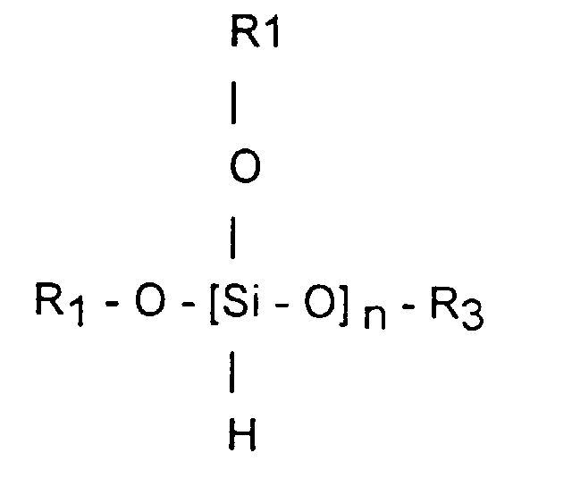
- Procédé selon l'une quelconque des revendications 7 ou 8, caractérisé en ce que le composé organo-silicé est choisi parmi les alkoxysilanes de formule :avec n inférieur ou égal à 5

les siloxanes de formuleavec n inférieur ou égal à 4
ou les silazanes de formuleavec n inférieur à 4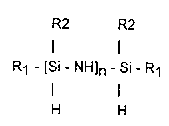
- Procédé selon la revendication 9, caractérisé en ce que le composé organo-silicé est du tétraméthyldisiloxane.
- Procédé selon l'une quelconque des revendications 7 à 10, caractérisé en ce que le gaz précurseur des éléments conducteurs est un complexe métallique.
- Procédé selon la revendication 11, caractérisé en ce que le complexe métallique est un métal carbonyle.
- Procédé selon la revendication 11, caractérisé en ce que le complexe métallique est un acétyle acétonate ou un fluoro-acétyle acétonate.
- Procédé selon l'une quelconque des revendications 7 à 10, caractérisé en ce que le gaz précurseur des éléments conducteurs est de l'hydrogène sulfureux.
- Procédé selon l'un quelconque des revendications 7 à 10, caractérisé en ce que le gaz précurseur des éléments conducteurs est du dichlorure de soufre.
- Procédé selon l'une quelconque des revendications 7 à 15, caractérisé en ce que la pression de l'azote est comprise entre 1 hPa et 20 hPa.
- Procédé selon l'une quelconque des revendications 7 à 16, caractérisé en ce qu'il comprend la présence d'oxygène lors du dépôt des couches diélectriques.
- Procédé selon l'une quelconque des revendications 6 à 17, caractérisé en ce que le dépôt des couches diélectriques et des couches conductrices s'effectue sur un substrat diélectrique (1) placé à la surface d'un tambour (2) en rotation, ladite rotation s'effectuant de façon qu'une même portion du substrat diélectrique (1) se trouve successivement en regard d'au moins un dispositif (C1, 8, 7) de dépôt de diélectrique et d'au moins un dispositif (C2, 8, 7) de dépôt d'éléments conducteurs, chaque dépôt de diélectrique ou de conducteur étant précédé d'un masquage des zones où ledit dépôt n'est pas autorisé.
- Procédé selon la revendication 18, caractérisé en ce que ledit masquage est réalisé par dépôt d'huile.
- Procédé selon la revendication 19, caractérisé en ce que ledit dépôt d'huile est réalisé par un dispositif de masquage constitué d'un rouleau d'impression sur lequel sont formées des encoches, lesdites encoches s'emplissant d'huile en phase vapeur, ladite huile en phase vapeur se déposant par condensation.
- Procédé selon la revendication 20, caractérisé en ce que le masquage des zones où les dépôts de diélectrique et de polymère conducteur ne sont pas autorisés conduit à la fabrication d'une structure capacitive constituée de N structures capacitives élémentaires (Si, 1 = 1, 2, ... N) en parallèle séparées les unes des autres par des puits (Pi, 1 = 1, 2, ..., N-1), chaque structure capacitive élémentaire ayant ses parois latérales conductrices.
- Procédé selon la revendication 21, caractérisé en ce qu'il comprend une étape de découpe de ladite structure capacitive en lesdites N structures capacitives élémentaires, ladite découpe étant réalisée par des éléments coupants solidaires du rouleau d'impression.
- Procédé selon la revendication 22, caractérisé en ce que chaque structure capacitive élémentaire issue de ladite découpe est passée dans une vague d'alliage en fusion afin de constituer les armatures des futurs condensateurs.
- Procédé selon la revendication 22, caractérisé en ce qu'il comprend le dépôt d'un alliage à braser sur les parois latérales de chaque structure capacitive élémentaire issue de ladite découpe afin de constituer les armatures des futurs condensateurs.
- Procédé selon l'une quelconque des revendications 23 ou 24, caractérisé en ce qu'il comprend la découpe des structures capacitives élémentaires en condensateurs élémentaires.
- Procédé selon la revendication 20, caractérisé en ce que le masquage des zones où les dépôts de diélectrique et de polymère conducteur ne sont pas autorisés conduit à la fabrication d'une structure résistive constituée de N structures résistives élémentaires (Ri, 1 = 1, 2, ..., N) séparées les unes des autres par des puits (Pi, 1 = 1, 2, N - 1), chaque structure résistive élémentaire ayant ses parois latérales conductrices et électriquement reliées entre elles.
- Procédé selon la revendication 26, caractérisé en ce qu'il comprend une étape de découpe de ladite structure résistive en lesdites N structures résistives élémentaires, ladite découpe étant réalisée par des éléments coupants solidaires du rouleau d'impression.
- Procédé selon la revendication 27, caractérisé en ce que chaque structure résistive élémentaire (Ri, 1 = 1, 2, ..., N) issue de ladite découpe est passée dans une vague d'alliage en fusion afin de constituer les connexions des futures résistances.
- Procédé selon la revendication 27, caractérisé en ce qu'il comprend le dépôt d'un alliage à braser sur les parois latérales de chaque structure élémentaire issue de ladite découpe afin de constituer les bornes des futures résistances.
- Procédé selon la revendication 28 ou 29, caractérisé en ce qu'il comprend la découpe de chaque structure résistive élémentaire en résistances élémentaires.
- Procédé selon la revendication 20, caractérisé en ce que le masquage des zones où les dépôts de diélectrique et de polymère conducteur ne sont pas autorisés conduit à la fabrication d'une structure constituée d'une succession de structures élémentaires capacitives et résistives, chaque structure élémentaire capacitive et résistive ayant ses parois latérales conductrices, chaque structure élémentaire résistive ayant ses parois latérales électriquement reliées entre elles.
- Procédé selon la revendication 31, caractérisé en ce qu'il comprend une étape de découpe de ladite structure en structures élémentaires constituées chacune d'une structure élémentaire capacitive et d'une structure élémentaire résistive.
- Procédé selon la revendication 32, caractérisé en ce que chaque structure élémentaire est passée dans une vague d'alliage en fusion afin de constituer les connexions des futurs composants.
- Procédé selon la revendication 33, caractérisé en ce qu'il comprend le dépôt d'un alliage à braser sur les parois latérales desdites structures élémentaires.
- Procédé selon la revendication 34, caractérisé en ce qu'il comprend la découpe des structures élémentaires de façon à constituer des composants formés d'une capacité et d'une résistance en série.
- Condensateur de type empilé constitué d'une alternance de couches diélectriques de rang impair et pair et de couches conductrices de rang impair et pair, ledit condensateur empilé constituant une structure ayant deux faces latérales opposées recouvertes de matériau conducteur, caractérisé en ce que les couches diélectriques sont obtenues par dépôts d'éléments diélectriques en couche mince et les couches conductrices par dépôts d'éléments conducteurs en couche mince, le recouvrement de matériau conducteur d'une première face latérale étant obtenu par lesdits dépôts d'éléments conducteurs de façon à relier électriquement entre elles les couches conductrices de rang pair et le recouvrement de matériau conducteur de la face latérale opposée à ladite première face étant obtenu par lesdits dépôts d'éléments conducteurs de façon à relier électriquement entre elle les couches conductrices de rang impair.
- Résistance caractérisée en ce qu'elle est constituée d'une alternance de couches diélectriques de rang impair et pair et de couches conductrices de rang impair et pair, ladite alternance constituant une structure ayant deux faces latérales opposées recouvertes de matériau conducteur, les couches diélectriques étant obtenues par dépôts d'éléments diélectriques en couche mince et les couches conductrices par dépôt d'éléments conducteurs en couche mince, chaque couche conductrice ayant une première extrémité située sur une première face latérale et une deuxième extrémité située sur une deuxième face latérale opposée à la première face latérale, une couche conductrice de rang impair ayant sa première extrémité électriquement reliée à la première extrémité de la couche conductrice de rang pair immédiatement au-dessus et une couche conductrice de rang pair ayant sa deuxième extrémité électriquement reliée à la deuxième extrémité de la couche conductrice de rang impair immédiatement au-dessus, les liaisons électriques entre lesdites extrémités étant réalisées lors du dépôt des couches conductrices.
- Composant électronique, caractérisé en ce qu'il est constitué d'au moins un condensateur selon la revendication 36 et d'au moins une résistance selon la revendication 37.
Applications Claiming Priority (3)
| Application Number | Priority Date | Filing Date | Title |
|---|---|---|---|
| FR9314520A FR2713389B1 (fr) | 1993-12-03 | 1993-12-03 | Procédé de fabrication de composant de type empilé. |
| FR9314520 | 1993-12-03 | ||
| PCT/FR1994/001405 WO1995015571A1 (fr) | 1993-12-03 | 1994-12-01 | Composant de type empile et procede de fabrication de composant de type empile |
Publications (2)
| Publication Number | Publication Date |
|---|---|
| EP0731975A1 EP0731975A1 (fr) | 1996-09-18 |
| EP0731975B1 true EP0731975B1 (fr) | 1999-01-20 |
Family
ID=9453536
Family Applications (1)
| Application Number | Title | Priority Date | Filing Date |
|---|---|---|---|
| EP95902823A Expired - Lifetime EP0731975B1 (fr) | 1993-12-03 | 1994-12-01 | Composant de type empile et procede de fabrication de composant de type empile |
Country Status (10)
| Country | Link |
|---|---|
| EP (1) | EP0731975B1 (fr) |
| JP (1) | JPH09505944A (fr) |
| KR (1) | KR960706684A (fr) |
| AT (1) | ATE176080T1 (fr) |
| CA (1) | CA2177986A1 (fr) |
| DE (1) | DE69416163T2 (fr) |
| ES (1) | ES2129796T3 (fr) |
| FI (1) | FI962294A7 (fr) |
| FR (1) | FR2713389B1 (fr) |
| WO (1) | WO1995015571A1 (fr) |
Families Citing this family (3)
| Publication number | Priority date | Publication date | Assignee | Title |
|---|---|---|---|---|
| AUPN363595A0 (en) * | 1995-06-19 | 1995-07-13 | Intag International Limited | Fabrication of capacitors |
| US7129187B2 (en) * | 2004-07-14 | 2006-10-31 | Tokyo Electron Limited | Low-temperature plasma-enhanced chemical vapor deposition of silicon-nitrogen-containing films |
| JP7823398B2 (ja) * | 2022-01-13 | 2026-03-04 | 富士電機株式会社 | 半導体装置 |
Family Cites Families (1)
| Publication number | Priority date | Publication date | Assignee | Title |
|---|---|---|---|---|
| US4599678A (en) * | 1985-03-19 | 1986-07-08 | Wertheimer Michael R | Plasma-deposited capacitor dielectrics |
-
1993
- 1993-12-03 FR FR9314520A patent/FR2713389B1/fr not_active Expired - Fee Related
-
1994
- 1994-12-01 KR KR1019960702985A patent/KR960706684A/ko not_active Withdrawn
- 1994-12-01 FI FI962294A patent/FI962294A7/fi not_active Application Discontinuation
- 1994-12-01 ES ES95902823T patent/ES2129796T3/es not_active Expired - Lifetime
- 1994-12-01 AT AT95902823T patent/ATE176080T1/de active
- 1994-12-01 JP JP7515451A patent/JPH09505944A/ja active Pending
- 1994-12-01 CA CA002177986A patent/CA2177986A1/fr not_active Abandoned
- 1994-12-01 EP EP95902823A patent/EP0731975B1/fr not_active Expired - Lifetime
- 1994-12-01 DE DE69416163T patent/DE69416163T2/de not_active Expired - Fee Related
- 1994-12-01 WO PCT/FR1994/001405 patent/WO1995015571A1/fr not_active Ceased
Also Published As
| Publication number | Publication date |
|---|---|
| ATE176080T1 (de) | 1999-02-15 |
| EP0731975A1 (fr) | 1996-09-18 |
| WO1995015571A1 (fr) | 1995-06-08 |
| DE69416163D1 (de) | 1999-03-04 |
| DE69416163T2 (de) | 1999-09-02 |
| JPH09505944A (ja) | 1997-06-10 |
| FI962294L (fi) | 1996-07-22 |
| CA2177986A1 (fr) | 1995-06-08 |
| FI962294A0 (fi) | 1996-05-31 |
| ES2129796T3 (es) | 1999-06-16 |
| FI962294A7 (fi) | 1996-07-22 |
| FR2713389A1 (fr) | 1995-06-09 |
| FR2713389B1 (fr) | 1996-01-26 |
| KR960706684A (ko) | 1996-12-09 |
Similar Documents
| Publication | Publication Date | Title |
|---|---|---|
| CA2119852C (fr) | Procede et dispositif pour le revetement en continu d'un materiau metallique en defilement par un depot de polymere a gradient de composition, et produit obtenu par ce procede | |
| EP0201422B1 (fr) | Pile solide intégrable et procédé de réalisation | |
| EP2962345B1 (fr) | Procede de fabrication d'une batterie monolithique entierement solide | |
| EP1970950B1 (fr) | Procédé de fabrication d'une structure d'interconnexions à cavités d'air pour circuit intégré | |
| WO1997024753A1 (fr) | Transistor a couches minces et procede de depot d'au moins une couche semi-conductrice pour la realisation de ce transistor | |
| EP3903362A1 (fr) | Procédé de fabrication de batteries, et batterie obtenue par ce procédé | |
| EP0731975A1 (fr) | Composant de type empile et procede de fabrication de composant de type empile | |
| EP1941569B1 (fr) | Electrode pour pile a combustible alcaline et procede de fabrication d'une pile a combustible comportant au moins une etape de fabrication d'une telle electrode | |
| EP0681746B1 (fr) | Composant piezoelectrique et procede de sa fabrication | |
| EP0731974A1 (fr) | Procede de fabrication de condensateur et condensateur issu d'un tel procede | |
| FR2718154A1 (fr) | Procédé de dépôt de diélectrique et/ou de métal sur un substrat. | |
| FR3105604A1 (fr) | Batterie avec un systeme d’encapsulation renforcee au niveau des organes de contact | |
| FR2659485A1 (fr) | Condensateur a film dielectrique souple metallise et procede de realisation d'un tel condensateur. | |
| CA2167316A1 (fr) | Procede de fabrication de condensateur et condensateur issu d'un tel procede | |
| FR2718155A1 (fr) | Procédé de dépôt de diélectrique et/ou de métal sur un substrat. | |
| FR2538110A1 (fr) | Jauge piezoresistive et son procede de fabrication | |
| FR3105605A1 (fr) | Batterie, notamment en couches minces, avec un nouveau système d’encapsulation | |
| EP4685900A1 (fr) | Électrolyte solide comprenant un revêtement métallique et procédés de fabrication d'un tel électrolyte solide | |
| FR2726151A1 (fr) | Procede et dispositif de protection hermetique de circuit electronique | |
| FR3148494A1 (fr) | Structure comprenant une couche diélectrique ionique ultramince et son procédé de fabrication | |
| FR2490021A1 (fr) | Dispositif du type cellule electrochimique a electrolyte solide et son procede de fabrication | |
| CN111542938A (zh) | 蓄电装置 | |
| Simon et al. | Tenue en tension dans le vide entre electrodes ecartees de 10 millimetres: Etudes de differents materiaux et influence de l'energie disponible | |
| BE676515A (fr) |
Legal Events
| Date | Code | Title | Description |
|---|---|---|---|
| PUAI | Public reference made under article 153(3) epc to a published international application that has entered the european phase |
Free format text: ORIGINAL CODE: 0009012 |
|
| 17P | Request for examination filed |
Effective date: 19960402 |
|
| AK | Designated contracting states |
Kind code of ref document: A1 Designated state(s): AT BE CH DE ES FR GB IE IT LI LU NL SE |
|
| 17Q | First examination report despatched |
Effective date: 19961105 |
|
| GRAG | Despatch of communication of intention to grant |
Free format text: ORIGINAL CODE: EPIDOS AGRA |
|
| GRAG | Despatch of communication of intention to grant |
Free format text: ORIGINAL CODE: EPIDOS AGRA |
|
| GRAH | Despatch of communication of intention to grant a patent |
Free format text: ORIGINAL CODE: EPIDOS IGRA |
|
| GRAH | Despatch of communication of intention to grant a patent |
Free format text: ORIGINAL CODE: EPIDOS IGRA |
|
| GRAA | (expected) grant |
Free format text: ORIGINAL CODE: 0009210 |
|
| AK | Designated contracting states |
Kind code of ref document: B1 Designated state(s): AT BE CH DE ES FR GB IE IT LI LU NL SE |
|
| REF | Corresponds to: |
Ref document number: 176080 Country of ref document: AT Date of ref document: 19990215 Kind code of ref document: T |
|
| REG | Reference to a national code |
Ref country code: CH Ref legal event code: EP |
|
| REG | Reference to a national code |
Ref country code: IE Ref legal event code: FG4D Free format text: FRENCH |
|
| REF | Corresponds to: |
Ref document number: 69416163 Country of ref document: DE Date of ref document: 19990304 |
|
| ITF | It: translation for a ep patent filed | ||
| PG25 | Lapsed in a contracting state [announced via postgrant information from national office to epo] |
Ref country code: DE Free format text: LAPSE BECAUSE OF FAILURE TO SUBMIT A TRANSLATION OF THE DESCRIPTION OR TO PAY THE FEE WITHIN THE PRESCRIBED TIME-LIMIT Effective date: 19990421 |
|
| RAP2 | Party data changed (patent owner data changed or rights of a patent transferred) |
Owner name: THOMSON-CSF PASSIVE COMPONENTS TPC |
|
| GBT | Gb: translation of ep patent filed (gb section 77(6)(a)/1977) |
Effective date: 19990513 |
|
| REG | Reference to a national code |
Ref country code: ES Ref legal event code: FG2A Ref document number: 2129796 Country of ref document: ES Kind code of ref document: T3 |
|
| NLT2 | Nl: modifications (of names), taken from the european patent patent bulletin |
Owner name: THOMSON-CSF PASSIVE COMPONENTS "TPC" |
|
| PLBE | No opposition filed within time limit |
Free format text: ORIGINAL CODE: 0009261 |
|
| STAA | Information on the status of an ep patent application or granted ep patent |
Free format text: STATUS: NO OPPOSITION FILED WITHIN TIME LIMIT |
|
| 26N | No opposition filed | ||
| NLT1 | Nl: modifications of names registered in virtue of documents presented to the patent office pursuant to art. 16 a, paragraph 1 |
Owner name: THOMSON-CSF PASSIVE COMPONENTS "TPC" |
|
| PGFP | Annual fee paid to national office [announced via postgrant information from national office to epo] |
Ref country code: CH Payment date: 20001120 Year of fee payment: 7 |
|
| PGFP | Annual fee paid to national office [announced via postgrant information from national office to epo] |
Ref country code: IE Payment date: 20001121 Year of fee payment: 7 |
|
| PGFP | Annual fee paid to national office [announced via postgrant information from national office to epo] |
Ref country code: DE Payment date: 20001122 Year of fee payment: 7 |
|
| PGFP | Annual fee paid to national office [announced via postgrant information from national office to epo] |
Ref country code: NL Payment date: 20001123 Year of fee payment: 7 |
|
| PGFP | Annual fee paid to national office [announced via postgrant information from national office to epo] |
Ref country code: SE Payment date: 20001124 Year of fee payment: 7 Ref country code: GB Payment date: 20001124 Year of fee payment: 7 |
|
| PGFP | Annual fee paid to national office [announced via postgrant information from national office to epo] |
Ref country code: LU Payment date: 20001127 Year of fee payment: 7 |
|
| PGFP | Annual fee paid to national office [announced via postgrant information from national office to epo] |
Ref country code: ES Payment date: 20001218 Year of fee payment: 7 |
|
| PGFP | Annual fee paid to national office [announced via postgrant information from national office to epo] |
Ref country code: FR Payment date: 20001221 Year of fee payment: 7 |
|
| PGFP | Annual fee paid to national office [announced via postgrant information from national office to epo] |
Ref country code: AT Payment date: 20001229 Year of fee payment: 7 |
|
| PGFP | Annual fee paid to national office [announced via postgrant information from national office to epo] |
Ref country code: BE Payment date: 20010119 Year of fee payment: 7 |
|
| PG25 | Lapsed in a contracting state [announced via postgrant information from national office to epo] |
Ref country code: LU Free format text: LAPSE BECAUSE OF NON-PAYMENT OF DUE FEES Effective date: 20011201 Ref country code: GB Free format text: LAPSE BECAUSE OF NON-PAYMENT OF DUE FEES Effective date: 20011201 Ref country code: AT Free format text: LAPSE BECAUSE OF NON-PAYMENT OF DUE FEES Effective date: 20011201 |
|
| PG25 | Lapsed in a contracting state [announced via postgrant information from national office to epo] |
Ref country code: SE Free format text: LAPSE BECAUSE OF NON-PAYMENT OF DUE FEES Effective date: 20011202 |
|
| PG25 | Lapsed in a contracting state [announced via postgrant information from national office to epo] |
Ref country code: IE Free format text: LAPSE BECAUSE OF FAILURE TO SUBMIT A TRANSLATION OF THE DESCRIPTION OR TO PAY THE FEE WITHIN THE PRESCRIBED TIME-LIMIT Effective date: 20011203 |
|
| PG25 | Lapsed in a contracting state [announced via postgrant information from national office to epo] |
Ref country code: LI Free format text: LAPSE BECAUSE OF NON-PAYMENT OF DUE FEES Effective date: 20011231 Ref country code: CH Free format text: LAPSE BECAUSE OF NON-PAYMENT OF DUE FEES Effective date: 20011231 Ref country code: BE Free format text: LAPSE BECAUSE OF NON-PAYMENT OF DUE FEES Effective date: 20011231 |
|
| REG | Reference to a national code |
Ref country code: GB Ref legal event code: IF02 |
|
| BERE | Be: lapsed |
Owner name: CIE EUROPEENNE DE COMPOSANTS ELECTRONIQUES LCC Effective date: 20011231 |
|
| PG25 | Lapsed in a contracting state [announced via postgrant information from national office to epo] |
Ref country code: NL Free format text: LAPSE BECAUSE OF NON-PAYMENT OF DUE FEES Effective date: 20020701 |
|
| GBPC | Gb: european patent ceased through non-payment of renewal fee |
Effective date: 20011201 |
|
| EUG | Se: european patent has lapsed |
Ref document number: 95902823.4 |
|
| REG | Reference to a national code |
Ref country code: CH Ref legal event code: PL |
|
| PG25 | Lapsed in a contracting state [announced via postgrant information from national office to epo] |
Ref country code: FR Free format text: LAPSE BECAUSE OF NON-PAYMENT OF DUE FEES Effective date: 20020830 |
|
| NLV4 | Nl: lapsed or anulled due to non-payment of the annual fee |
Effective date: 20020701 |
|
| REG | Reference to a national code |
Ref country code: FR Ref legal event code: ST |
|
| REG | Reference to a national code |
Ref country code: IE Ref legal event code: MM4A |
|
| PG25 | Lapsed in a contracting state [announced via postgrant information from national office to epo] |
Ref country code: ES Free format text: LAPSE BECAUSE OF NON-PAYMENT OF DUE FEES Effective date: 20021202 |
|
| REG | Reference to a national code |
Ref country code: ES Ref legal event code: FD2A Effective date: 20030113 |
|
| PG25 | Lapsed in a contracting state [announced via postgrant information from national office to epo] |
Ref country code: IT Free format text: LAPSE BECAUSE OF NON-PAYMENT OF DUE FEES;WARNING: LAPSES OF ITALIAN PATENTS WITH EFFECTIVE DATE BEFORE 2007 MAY HAVE OCCURRED AT ANY TIME BEFORE 2007. THE CORRECT EFFECTIVE DATE MAY BE DIFFERENT FROM THE ONE RECORDED. Effective date: 20051201 |