EP0731509B1 - Optoelectronic converter and process of manufacturing - Google Patents
Optoelectronic converter and process of manufacturing Download PDFInfo
- Publication number
- EP0731509B1 EP0731509B1 EP96103353A EP96103353A EP0731509B1 EP 0731509 B1 EP0731509 B1 EP 0731509B1 EP 96103353 A EP96103353 A EP 96103353A EP 96103353 A EP96103353 A EP 96103353A EP 0731509 B1 EP0731509 B1 EP 0731509B1
- Authority
- EP
- European Patent Office
- Prior art keywords
- baseplate
- plate
- transducer according
- semiconductor component
- silicon
- Prior art date
- Legal status (The legal status is an assumption and is not a legal conclusion. Google has not performed a legal analysis and makes no representation as to the accuracy of the status listed.)
- Expired - Lifetime
Links
- 230000005693 optoelectronics Effects 0.000 title claims description 14
- 238000000034 method Methods 0.000 title claims description 8
- 238000004519 manufacturing process Methods 0.000 title claims description 6
- 239000004065 semiconductor Substances 0.000 claims description 37
- 125000006850 spacer group Chemical group 0.000 claims description 23
- 239000010703 silicon Substances 0.000 claims description 20
- 229910052710 silicon Inorganic materials 0.000 claims description 20
- 239000011521 glass Substances 0.000 claims description 18
- 239000000463 material Substances 0.000 claims description 6
- 239000002131 composite material Substances 0.000 claims description 4
- 239000002184 metal Substances 0.000 claims description 2
- NJPPVKZQTLUDBO-UHFFFAOYSA-N novaluron Chemical compound C1=C(Cl)C(OC(F)(F)C(OC(F)(F)F)F)=CC=C1NC(=O)NC(=O)C1=C(F)C=CC=C1F NJPPVKZQTLUDBO-UHFFFAOYSA-N 0.000 claims 3
- 239000000969 carrier Substances 0.000 claims 1
- XUIMIQQOPSSXEZ-UHFFFAOYSA-N Silicon Chemical compound [Si] XUIMIQQOPSSXEZ-UHFFFAOYSA-N 0.000 description 16
- 230000005855 radiation Effects 0.000 description 6
- 238000005476 soldering Methods 0.000 description 5
- 238000004026 adhesive bonding Methods 0.000 description 4
- 238000001465 metallisation Methods 0.000 description 3
- 239000013307 optical fiber Substances 0.000 description 3
- 239000010410 layer Substances 0.000 description 2
- 229910000679 solder Inorganic materials 0.000 description 2
- RZVAJINKPMORJF-UHFFFAOYSA-N Acetaminophen Chemical compound CC(=O)NC1=CC=C(O)C=C1 RZVAJINKPMORJF-UHFFFAOYSA-N 0.000 description 1
- 239000002313 adhesive film Substances 0.000 description 1
- 239000012790 adhesive layer Substances 0.000 description 1
- 239000005388 borosilicate glass Substances 0.000 description 1
- 230000001419 dependent effect Effects 0.000 description 1
- 238000011161 development Methods 0.000 description 1
- 230000018109 developmental process Effects 0.000 description 1
- 238000005530 etching Methods 0.000 description 1
- 230000017525 heat dissipation Effects 0.000 description 1
- 238000012986 modification Methods 0.000 description 1
- 230000004048 modification Effects 0.000 description 1
- 239000005297 pyrex Substances 0.000 description 1
- 238000006748 scratching Methods 0.000 description 1
- 230000002393 scratching effect Effects 0.000 description 1
- 238000000926 separation method Methods 0.000 description 1
Images

Classifications
-
- H—ELECTRICITY
- H01—ELECTRIC ELEMENTS
- H01L—SEMICONDUCTOR DEVICES NOT COVERED BY CLASS H10
- H01L31/00—Semiconductor devices sensitive to infrared radiation, light, electromagnetic radiation of shorter wavelength or corpuscular radiation and specially adapted either for the conversion of the energy of such radiation into electrical energy or for the control of electrical energy by such radiation; Processes or apparatus specially adapted for the manufacture or treatment thereof or of parts thereof; Details thereof
- H01L31/0248—Semiconductor devices sensitive to infrared radiation, light, electromagnetic radiation of shorter wavelength or corpuscular radiation and specially adapted either for the conversion of the energy of such radiation into electrical energy or for the control of electrical energy by such radiation; Processes or apparatus specially adapted for the manufacture or treatment thereof or of parts thereof; Details thereof characterised by their semiconductor bodies
- H01L31/0256—Semiconductor devices sensitive to infrared radiation, light, electromagnetic radiation of shorter wavelength or corpuscular radiation and specially adapted either for the conversion of the energy of such radiation into electrical energy or for the control of electrical energy by such radiation; Processes or apparatus specially adapted for the manufacture or treatment thereof or of parts thereof; Details thereof characterised by their semiconductor bodies characterised by the material
- H01L31/0264—Inorganic materials
- H01L31/032—Inorganic materials including, apart from doping materials or other impurities, only compounds not provided for in groups H01L31/0272 - H01L31/0312
-
- H—ELECTRICITY
- H01—ELECTRIC ELEMENTS
- H01L—SEMICONDUCTOR DEVICES NOT COVERED BY CLASS H10
- H01L33/00—Semiconductor devices with at least one potential-jump barrier or surface barrier specially adapted for light emission; Processes or apparatus specially adapted for the manufacture or treatment thereof or of parts thereof; Details thereof
- H01L33/48—Semiconductor devices with at least one potential-jump barrier or surface barrier specially adapted for light emission; Processes or apparatus specially adapted for the manufacture or treatment thereof or of parts thereof; Details thereof characterised by the semiconductor body packages
- H01L33/58—Optical field-shaping elements
-
- G—PHYSICS
- G02—OPTICS
- G02B—OPTICAL ELEMENTS, SYSTEMS OR APPARATUS
- G02B6/00—Light guides; Structural details of arrangements comprising light guides and other optical elements, e.g. couplings
- G02B6/24—Coupling light guides
- G02B6/42—Coupling light guides with opto-electronic elements
- G02B6/4201—Packages, e.g. shape, construction, internal or external details
- G02B6/4204—Packages, e.g. shape, construction, internal or external details the coupling comprising intermediate optical elements, e.g. lenses, holograms
-
- H—ELECTRICITY
- H01—ELECTRIC ELEMENTS
- H01L—SEMICONDUCTOR DEVICES NOT COVERED BY CLASS H10
- H01L31/00—Semiconductor devices sensitive to infrared radiation, light, electromagnetic radiation of shorter wavelength or corpuscular radiation and specially adapted either for the conversion of the energy of such radiation into electrical energy or for the control of electrical energy by such radiation; Processes or apparatus specially adapted for the manufacture or treatment thereof or of parts thereof; Details thereof
- H01L31/02—Details
- H01L31/0203—Containers; Encapsulations, e.g. encapsulation of photodiodes
-
- H—ELECTRICITY
- H01—ELECTRIC ELEMENTS
- H01L—SEMICONDUCTOR DEVICES NOT COVERED BY CLASS H10
- H01L31/00—Semiconductor devices sensitive to infrared radiation, light, electromagnetic radiation of shorter wavelength or corpuscular radiation and specially adapted either for the conversion of the energy of such radiation into electrical energy or for the control of electrical energy by such radiation; Processes or apparatus specially adapted for the manufacture or treatment thereof or of parts thereof; Details thereof
- H01L31/02—Details
- H01L31/0232—Optical elements or arrangements associated with the device
- H01L31/02325—Optical elements or arrangements associated with the device the optical elements not being integrated nor being directly associated with the device
-
- H—ELECTRICITY
- H01—ELECTRIC ELEMENTS
- H01L—SEMICONDUCTOR DEVICES NOT COVERED BY CLASS H10
- H01L2224/00—Indexing scheme for arrangements for connecting or disconnecting semiconductor or solid-state bodies and methods related thereto as covered by H01L24/00
- H01L2224/01—Means for bonding being attached to, or being formed on, the surface to be connected, e.g. chip-to-package, die-attach, "first-level" interconnects; Manufacturing methods related thereto
- H01L2224/26—Layer connectors, e.g. plate connectors, solder or adhesive layers; Manufacturing methods related thereto
- H01L2224/31—Structure, shape, material or disposition of the layer connectors after the connecting process
- H01L2224/32—Structure, shape, material or disposition of the layer connectors after the connecting process of an individual layer connector
- H01L2224/321—Disposition
- H01L2224/32151—Disposition the layer connector connecting between a semiconductor or solid-state body and an item not being a semiconductor or solid-state body, e.g. chip-to-substrate, chip-to-passive
- H01L2224/32221—Disposition the layer connector connecting between a semiconductor or solid-state body and an item not being a semiconductor or solid-state body, e.g. chip-to-substrate, chip-to-passive the body and the item being stacked
- H01L2224/32225—Disposition the layer connector connecting between a semiconductor or solid-state body and an item not being a semiconductor or solid-state body, e.g. chip-to-substrate, chip-to-passive the body and the item being stacked the item being non-metallic, e.g. insulating substrate with or without metallisation
Definitions
- the invention relates to an optoelectronic Transducer with a radiation receiving or emitting Semiconductor component, with a base plate on which the Semiconductor component is attached and with a Carrier plate connected spacer for an optically the semiconductor component aligned lens system, wherein the base plate, the spacer and the lens system Materials with at least similar thermal Expansion coefficients exist.
- Such converters are known, for example, from US Pat. No. 4,055,761 or US Pat JP 5-218 463 known.
- JP-A-7040589 and JP-A-6326831 Display devices described in which on a base plate a lens plate is attached by means of spacers. Bottom plate, spacing and lens plate almost point the same thermal expansion coefficient.
- a major problem is the converter with good To operate efficiency. This will, apart from the Properties of the semiconductor device itself, thereby achieved that the lens system optically optimal on the Semiconductor device is aligned. Only then can the light from the semiconductor device with high efficiency decouple an optical fiber or from an optical fiber couple the semiconductor device.
- the invention has for its object an optoelectronic To improve transducers of the type mentioned at the beginning, that temperature fluctuations have little impact on the adjustment between the semiconductor component and the lens system to have.
- a simple procedure for Manufacture of such an optoelectronic converter specified become.
- the first-mentioned goal is achieved in that the base plate, the spacer and lens system made of materials with at least similar coefficients of thermal expansion consist.
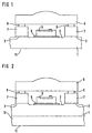
- the optoelectronic converter according to FIG. 1 is on one Base plate 1 built.
- the top surface of the bottom plate 1 is provided with depressions 2.
- On both sides of the depression 2 stays webs 3.
- a radiation receiving or emitting Semiconductor component 6 attached. This can e.g. a Photodiode or a light emitting diode (LED) or a Vertical cavity surface emitter laser (VCSEL).
- the Metallization 5 also serves to supply power to Semiconductor component 6.
- a second contact is on the Top of the semiconductor device.
- the webs 3 On the webs 3 are e.g. also web-shaped spacers 7 attached.
- a lens system lies on the spacers 7 8, which is integrally connected to the spacers is.
- the distance between the lens system and the bottom of the Recess 2 is larger than the thickness of the semiconductor component 6 plus the metal layer 5.
- the base plate 1 consists of silicon. This can be polycrystalline or be monocrystalline. Instead of silicon can also be a different material for the base plate 1 with a suitable coefficient of thermal expansion be used.
- the spacers 7 are made of glass, while the lens system can be made of silicon or glass. It is essential that at least one part consisting of glass is arranged between the semiconductor component and the lens system. Its low thermal conductivity prevents heat dissipated from the semiconductor component 6 into the base plate 1 from reaching the lens system. Because of its good thermal conductivity, a base plate made of silicon is preferably used for semiconductor components which emit radiation, since here the converted power is generally higher than in the case of radiation receivers. In the case of radiation receivers, the base plate 1 can be made of glass, the spacers 7 made of silicon and the lens system 8 made of silicon or glass. Silicon for the lens system in both cases can be preferred if the radiation has a wavelength for which silicon is transparent. This is the case for wavelengths greater than 1.1 ⁇ m .
- the base plate, the spacers 7 and the lens system 8 can be connected to each other by gluing and / or soldering become. If the silicon and glass surfaces lie on top of each other, they can also be bonded to one another by anodic bonding get connected. This technique is well known. there the parts to be bonded to one another at a temperature from e.g. 400 ° C pressed together and a tension e.g. of -1000 V is applied to the glass. When soldering or gluing spacers and The lens system becomes a solder or adhesive layer between the two parts 9 inserted. A solder layer can e.g. evaporated become.
- a type similar to silicon is used as the glass has coefficient of thermal expansion. Suitable for this e.g. a borosilicate glass that e.g. under the trade name "Pyrex" 7740 from Corning or Tempax from the Schott company comes onto the market.
- the optoelectronic converter (11) has a low capacitance instead of the silicon base plate is recommended a glass bottom plate.
- a silicon base plate so can be made thin and on the back with a Glass plate 10 ( Figure 2) are connected.
- the glass plate 10 can be done with the silicon bottom plate either by anodic Bonding, be connected by soldering or by gluing.
- the transducers 11 shown in Figures 1 and 2 are in one Housing used ( Figure 5), the base 14 and one Cover 15 has.
- the converter 11 becomes relative to one in the lid 15 attached window 16 adjusted and on the base 14 attached.
- An optical fiber bumps against the window (not shown) by a clutch 20 to the housing connected is.
- the semiconductor component itself is electrical over the metallization 5 and the one on the top of the Semiconductor component arranged contact with two connections 21 and 22 connected via which the operating voltage is supplied or the electrical signal is coupled out.
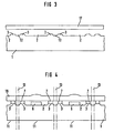
- the next step is a variety of lens systems containing plate 18 made of silicon or glass on the Spacer 7 placed.
- the lens systems are in one Grid arranged on the plate 18, the grid of the on the base plate 1 attached semiconductor device 6 corresponds.
- the lens systems are optically on the semiconductor components 6 aligned and then the plate 18 with the spacers 7 by the anodic described Bonding or connected by soldering. This creates a from base plate 1, semiconductor components 6, spacers 7 and plate 18 existing composite with a variety of Semiconductor components and lens systems.
- This association is then made by saw cuts 13 between the webs 3 and by right-angled, parallel to the drawing plane other saw cuts lying apart disassembled.
- Each of the resulting Units 11 are placed in a housing as described above used.
- the technique of dicing a wafer into small chips is has long been common in semiconductor technology and can be used in Separation of the network can also be applied.
- the So composite is divided by sawing, scratching and breaking. Here it is common to put the composite on an elastic Fix the adhesive film. The film then serves as a carrier all subsequent processes.
Description
Die Erfindung bezieht sich auf einen optoelektronischen Wandler mit einem Strahlung empfangenden oder aussendenden Halbleiterbauelement, mit einer Bodenplatte, auf dem das Halbleiterbauelement befestigt ist und mit einem mit der Trägerplatte verbundenen Abstandhalter für ein optisch auf das Halbleiterbauelement ausgerichtetes Linsensystem, wobei die Bodenplatte, der Abstandhalter und das Linsensystem aus Materialien mit zumindest ähnlichen thermischen Ausdehnungskoeffizienten bestehen.The invention relates to an optoelectronic Transducer with a radiation receiving or emitting Semiconductor component, with a base plate on which the Semiconductor component is attached and with a Carrier plate connected spacer for an optically the semiconductor component aligned lens system, wherein the base plate, the spacer and the lens system Materials with at least similar thermal Expansion coefficients exist.
Solche Wandler sind beispielsweise aus der US 4 055 761 oder der JP 5-218 463 bekannt.Such converters are known, for example, from US Pat. No. 4,055,761 or US Pat JP 5-218 463 known.
Weiterhin sind in der JP-A-7040589 und in der JP-A-6326831 Anzeigegeräte beschrieben, bei denen auf einer Bodenplatte mittels Abstandhalter eine Linsenplatte befestigt ist. Bodenplatte, Abstandhalten und Linsenplatte weisen nahezu denselben thermischen Ausdehnungskoeffiezienten auf.Furthermore, JP-A-7040589 and JP-A-6326831 Display devices described in which on a base plate a lens plate is attached by means of spacers. Bottom plate, spacing and lens plate almost point the same thermal expansion coefficient.
Ein wesentliches Problem besteht darin, die Wandler mit gutem Wirkungsgrad zu betreiben. Dies wird, abgesehen von den Eigenschaften des Halbleiterbauelements selbst, dadurch erreicht, daß das Linsensystem optisch optimal auf das Halbleiterbauelement ausgerichtet wird. Nur dann läßt sich das Licht vom Halbleiterbauelement mit hohem Wirkungsgrad auf einen Lichtleiter auskoppeln oder von einem Lichtleiter auf das Halbleiterbauelement einkoppeln.A major problem is the converter with good To operate efficiency. This will, apart from the Properties of the semiconductor device itself, thereby achieved that the lens system optically optimal on the Semiconductor device is aligned. Only then can the light from the semiconductor device with high efficiency decouple an optical fiber or from an optical fiber couple the semiconductor device.
Bei einem optoelektronischen Wandler muß außerdem sichergestellt werden, daß die optimale Justierung auch im Betrieb erhalten bleibt. Bei Erwärmung des Wandlers im Betrieb kann es nämlich zu Dejustierungen kommen, die den Wirkungsgrad verschlechtern.With an optoelectronic converter must also be ensured be that the optimal adjustment even in operation preserved. If the converter heats up during operation there are misalignments that affect efficiency worsen.
Der Erfindung liegt die Aufgabe zugrunde, einen optoelektronischen Wandler der eingangs erwähnten Art so zu verbessern, daß Temperaturschwankungen nur noch einen geringen Einfluß auf die Justierung zwischen Halbleiterbauelement und Linsensystem haben. Außerdem soll ein einfaches Verfahren zum Herstellen eines solchen optoelektronischen Wandlers angegeben werden. The invention has for its object an optoelectronic To improve transducers of the type mentioned at the beginning, that temperature fluctuations have little impact on the adjustment between the semiconductor component and the lens system to have. In addition, a simple procedure for Manufacture of such an optoelectronic converter specified become.
Das erstgenannte Ziel wird dadurch erreicht, daß die Bodenplatte, der Abstandhalter und das Linsensystem aus Materialien mit zumindest ähnlichen thermischen Ausdehnungskoeffizienten bestehen.The first-mentioned goal is achieved in that the base plate, the spacer and lens system made of materials with at least similar coefficients of thermal expansion consist.
Weiterbildungen der Erfindung sind Gegenstand der Unteransprüche
2 bis 8. Ein bevorzugtes Verfahren zur Herstellung
des optoelektonischen Wandlers ist Gegenstand des Anspruchs
9.Developments of the invention are the subject of the
Die Erfindung wird anhand zweier Ausführungsbeispiele in Verbindung mit den Figuren 1 bis 5 näher erläutert. Es zeigen
- Figur 1
- einen Schnitt durch ein erstes Ausführungsbeispiel,
Figur 2- einen Schnitt durch ein zweites Ausführungsbeispiel,
Figur 3 und 4- charakteristische Schritte bei der Herstellung des optoelektronischen Wandlers und
- Figur 5
- ein Gehäuse mit eingesetztem Wandler.
- Figure 1
- 2 shows a section through a first exemplary embodiment,
- Figure 2
- 2 shows a section through a second exemplary embodiment,
- Figures 3 and 4
- characteristic steps in the manufacture of the optoelectronic transducer and
- Figure 5
- a housing with inserted converter.
Der optoelektronische Wandler nach Figur 1 ist auf einer
Bodenplatte 1 aufgebaut. Die obere Oberfläche der Bodenplatte
1 ist mit Vertiefungen 2 versehen. Beidseitig der Vertiefung
2 bleiben Stege 3 stehen. In der Vertiefung 2 ist über eine
Metallisierung 5 ein Strahlung empfangendes oder aussendendes
Halbleiterbauelement 6 befestigt. Dieses kann z.B. eine
Fotodiode bzw. eine lichtaussendende Diode (LED) oder ein
Vertical Cavity Surface Emitter Laser (VCSEL) sein. Die
Metallisierung 5 dient außerdem zur Stromzuführung zum
Halbleiterbauelement 6. Ein zweiter Kontakt liegt auf der
Oberseite des Halbleiterbauelementes.The optoelectronic converter according to FIG. 1 is on one
Base plate 1 built. The top surface of the bottom plate
1 is provided with
Auf den Stegen 3 sind z.B. ebenfalls stegförmige Abstandhalter
7 befestigt. Auf den Abstandhaltern 7 liegt ein Linsensystem
8, das mit den Abstandhaltern stoffschlüssig verbunden
ist. Der Abstand zwischen dem Linsensystem und dem Boden der
Vertiefung 2 ist größer als die Dicke des Halbleiterbauelements
6 zuzüglich der Metallschicht 5. On the
Die Bodenplatte 1 besteht aus Silizium. Dieses kann polykristallin oder monokristallin sein. Anstelle von Silizium kann für die Bodenplatte 1 jedoch auch ein anderes Material mit einem geeigneten thermischen Ausdehnungskoeffizienten verwendet werden.The base plate 1 consists of silicon. This can be polycrystalline or be monocrystalline. Instead of silicon can also be a different material for the base plate 1 with a suitable coefficient of thermal expansion be used.
Die Abstandhalter 7 bestehen aus Glas, während das
Linsensystem aus Silizium oder Glas bestehen kann. Wesentlich
ist, daß zwischen dem Halbleiterbauelement und dem
Linsensystem wenigstens ein aus Glas bestehendes Teil
angeordnet ist. Dessen geringer Wärmeleitwert verhindert, daß
vom Halbleiterbauelement 6 in die Bodenplatte 1 abgeleitete
Wärme zum Linsensystem gelangt. Eine Bodenplatte aus Silizium
wird wegen ihrer guten Wärmeleitfähigkeit vorzugsweise bei
Strahlung aussendenden Halbleiterbauelementen verwendet, da
hier die umgesetzte Leistung i.a. höher als bei Strahlungsempfängern
ist. Bei Strahlungsempfängern kann die Bodenplatte
1 aus Glas bestehen, die Abstandhalter 7 aus Silizium und das
Linsensystem 8 aus Silizium oder Glas. Silizium für das
Linsensystem in beiden Fällen kann dann der Vorzug gegeben
werden, wenn die Strahlung eine Wellenlänge hat, für die
Silizium durchlässig ist. Dies ist bei Wellenlänge größer als
1,1 µm der Fall.The
Die Bodenplatte, die Abstandhalter 7 und das Linsensystem 8
können miteinander durch Kleben und/oder Löten verbunden
werden. Liegen jeweils Siliziumflächen und Glasflächen aufeinander,
so können diese auch durch anodisches Bonden miteinander
verbunden werden. Diese Technik ist bekannt. Dabei
werden die miteinander zu bondenden Teile unter einer Temperatur
von z.B. 400° C aufeinandergedrückt und eine Spannung
von z.B -1000 V wird am Glas angelegt.
Beim Löten oder Verkleben von Abstandhalter und
Linsensystem wird zwischen beide Teile eine Lot- oder Kleberschicht
9 eingefügt. Eine Lotschicht kann z.B. aufgedampft
werden.The base plate, the
Als Glas wird ein Typ verwendet, das ein dem Silizium ähnlichen thermischen Ausdehnungskoeffizienten hat. Hierfür eignet sich z.B ein Borosilikatglas, das z.B. unter der Handelsbezeichnung "Pyrex" 7740 von der Firma Corning oder Tempax von der Firma Schott in den Handel kommt.A type similar to silicon is used as the glass has coefficient of thermal expansion. Suitable for this e.g. a borosilicate glass that e.g. under the trade name "Pyrex" 7740 from Corning or Tempax from the Schott company comes onto the market.
Soll der optoelektronische Wandler (11) eine geringe Kapazität
haben, so empfiehlt sich statt der Silizium-Bodenplatte
eine Glas-Bodenplatte. Ist jedoch aus Gründen der besseren
Wärmeableitung eine Silizium-Bodenplatte erforderlich, so
kann diese dünn ausgeführt und auf ihrer Rückseite mit einer
Glasplatte 10 (Figur 2) verbunden werden. Die Glasplatte 10
kann mit der Siliziumbodenplatte entweder durch anodisches
Bonden, durch Löten oder durch Kleben verbunden sein.If the optoelectronic converter (11) has a low capacitance
instead of the silicon base plate is recommended
a glass bottom plate. However, for the sake of better
Heat dissipation required a silicon base plate, so
can be made thin and on the back with a
Glass plate 10 (Figure 2) are connected. The
Die in Figur 1 und 2 gezeigten Wandler 11 werden in ein
Gehäuse eingesetzt (Figur 5), das einen Sockel 14 und einen
Deckel 15 hat. Der Wandler 11 wird relativ zu einem im Deckel
15 angebrachtes Fenster 16 justiert und auf dem Sockel 14
befestigt. An das Fenster stößt ein Lichtwellenleiter (nicht
dargestellt), der durch eine Kupplung 20 mit dem Gehäuse
verbunden ist. Das Halbleiterbauelement selbst ist elektrisch
über die Metallisierung 5 und den auf der Oberseite des
Halbleiterbauelements angeordneten Kontakt mit zwei Anschlüssen
21 und 22 verbunden, über die die Betriebsspannung zugeführt
wird bzw. das elektrische Signal ausgekoppelt wird.The
Zum gleichzeitigen Herstellen einer Vielzahl von optoelektronischen
Wandlern 11 nach Figur 1 oder 2 wird zunächst eine
Glasplatte oder Siliziumplatte 1 mit Vertiefungen 2 versehen
(Figur 3). Diese Vertiefungen dienen der Aufnahme der Halbleiterbauelemente
und sind entsprechend breit bemessen.
Zwischen zwei der Vertiefungen 2 bleibt ein Steg stehen.
Diese Stege werden zweckmäßigerweise durch weitere Vertiefungen
12 voneinander getrennt, wodurch Stege 3 entstehen. Die
Vertiefungen 2, 12 können z.B. durch fotolithografisches
Ätzen oder durch Sägen hergestellt werden. Beim Sägen entstehen
einander parallele Stege 3, beim Ätzen können sie jede
beliebige Form, z.B. Gitterform annehmen.For the simultaneous production of a large number of
Als nächstes wird auf die Stege 3 eine aus Silizium oder Glas
bestehende Platte 17 aufgelegt und mit den Stegen wie beschrieben
durch anodisches Bonden, Kleben oder Verlöten
verbunden. Dann wird die Platte 17 zersägt derart, daß das
zwischen den Stegen 3 liegende, nicht mit der Bodenplatte 1
verbundenen Material entfernt wird. Dabei entstehen die mit
den Stegen 3 verbundenen Abstandhalter 7 (Figur 4). Anschließend
werden die Halbleiterbauelemente 6 gemäß einem
vorgegebenen Raster in den Vertiefungen 2 befestigt.Next, one is made of silicon or glass on the
Als nächster Schritt wird eine eine Vielzahl von Linsensystemen
enthaltende Platte 18 aus Silizium oder Glas auf die
Abstandhalter 7 aufgelegt. Die Linsensysteme sind in einem
Raster auf der Platte 18 angeordnet, das dem Raster der auf
der Bodenplatte 1 befestigten Halbleiterbauelement 6 entspricht.
Die Linsensysteme werden optisch auf die Halbleiterbauelemente
6 ausgerichtet und anschließend wird die Platte
18 mit den Abstandhaltern 7 durch das beschriebene anodische
Bonden oder durch Verlöten verbunden. Hierdurch entsteht ein
aus Bodenplatte 1, Halbleiterbauelementen 6, Abstandhaltern 7
und Platte 18 bestehender Verbund mit einer Vielzahl von
Halbleiterbauelementen und Linsensystemen. Dieser Verbund
wird dann durch zwischen den Stegen 3 gelegte Sägeschnitte 13
und durch dazu rechtwinklige, parallel zur Zeichenebene
liegende weitere Sägeschnitte zerlegt. Jede der dabei entstehenden
Einheiten 11 wird, wie oben beschrieben, in ein Gehäuse
eingesetzt.The next step is a variety of lens
Die Technik der Vereinzelung eines Wafers in kleine Chips ist in der Halbleitertechnik seit langem üblich und kann bei Vereinzelung des Verbundes ebenfalls angewandt werden. Der Verbund wird also durch Sägen, Ritzen und Brechen geteilt. Hierbei ist es üblich, den Verbund auf einer elastischen Klebefolie zu fixieren. Die Folie dient dann als Träger bei allen Nachfolgeprozessen.The technique of dicing a wafer into small chips is has long been common in semiconductor technology and can be used in Separation of the network can also be applied. The So composite is divided by sawing, scratching and breaking. Here it is common to put the composite on an elastic Fix the adhesive film. The film then serves as a carrier all subsequent processes.
Es ist in Abänderung des beschriebenen Verfahrens auch möglich,
zunächst fotolithografisch oder mechanisch die Vertiefungen
2 und die Stege 3 zu erzeugen und dann die Abstandhalter
wie beschrieben anzubringen. Anstelle einer mit vielen
Linsensystemen versehenen Scheibe 18 werden dann aber einzelne
Linsensysteme optisch auf die Halbleiterkörper ausgerichtet
und mit den Abstandhaltern 7 verbunden.In a modification of the method described, it is also possible
first the depressions, either photolithographically or mechanically
2 and to create the
Claims (10)
- Optoelectronic transducer having a radiation-receiving or -emitting semiconductor component having a baseplate (1) on which the semiconductor component (6) is fixed and having a spacer (7) connected to the baseplate (1), for a lens system (8) which is oriented optically towards the semiconductor component (6), the baseplate (1), the spacer (7) and the lens system (8) being composed of materials having at least similar thermal expansion coefficients,
characterized in that the spacer (7) is composed of glass. - Transducer according to Claim 1,
characterized in that the baseplate (1) and the lens system (8) are composed of silicon. - Transducer according to either of Claims 1 and 2,
characterized in that the baseplate (1) is provided with a metal layer (5) on which the semiconductor component (6) is fixed. - Transducer according to one of Claims 1 to 3,
characterized in that the parts composed of glass together with those composed of silicon are in each case connected to one another by anodic bonding. - Transducer according to one of Claims 1 to 4,
characterized in that respective parts composed of glass and/or of silicon are soldered or adhesively bonded to one another. - Transducer according to one of Claims 1 to 5,
characterized in that the semiconductor component (6) is seated in a depression (2) in the baseplate (1). - Transducer according to one of Claims 1 to 6,
characterized in that the baseplate (1) is composed of silicon, and in that the said baseplate is connected to a glass plate (10) on that side which is remote from the semiconductor component (6). - Optoelectronic component,
characterized in that an optoelectronic transducer according to one of Claims 1 to 7 is fixed on a pedestal (14) in a manner aligned relative to the window (16), in that a housing is provided which has the pedestal (14) and a cover (15) with a window (16). - Method for producing an optoelectronic transducer according to Claim 1,
characterized by the following features:a) depressions (2) for receiving the semiconductor components (6) are produced in the baseplate (1) in such a way that a web (3) remains at least on one side of each depression,b) a plate (17) of the size of the baseplate (1) is placed onto the webs and connected to the webs (3) by a material joint,c) the plate (17) is removed between the webs (3), thereby producing spacers (7) connected to the baseplate (1),d) the semiconductor components (6) are inserted into the depressions (2) in accordance with a predetermined grid pattern and connected to the baseplate (1),e) a further plate (18) is placed onto the carrier, which plate contains a number of lens systems (8) corresponding to the number of semiconductor components, which lens systems are arranged on the further plate in accordance with the same grid pattern,f) the further plate (18) is aligned with regard to the carrier in such a way that each of the lens systems is oriented towards one of the semiconductor components,g) the further plate (18) is fixed on the carriers,h) the composite comprising baseplate, semiconductor components, spacers and further plate is divided by first parallel cuts (13) and second cuts at right angles thereto, thereby producing units (11) each containing a baseplate (1), a semiconductor component (6), spacers (7) and a lens system (8). - Method according to Claim 9,
characterized in that each of the units (11) is inserted into a gas-tight housing (14, 15).
Applications Claiming Priority (2)
| Application Number | Priority Date | Filing Date | Title |
|---|---|---|---|
| DE19508222 | 1995-03-08 | ||
| DE19508222A DE19508222C1 (en) | 1995-03-08 | 1995-03-08 | Opto-electronic converter |
Publications (2)
| Publication Number | Publication Date |
|---|---|
| EP0731509A1 EP0731509A1 (en) | 1996-09-11 |
| EP0731509B1 true EP0731509B1 (en) | 2001-06-06 |
Family
ID=7756033
Family Applications (1)
| Application Number | Title | Priority Date | Filing Date |
|---|---|---|---|
| EP96103353A Expired - Lifetime EP0731509B1 (en) | 1995-03-08 | 1996-03-04 | Optoelectronic converter and process of manufacturing |
Country Status (8)
| Country | Link |
|---|---|
| US (1) | US5981945A (en) |
| EP (1) | EP0731509B1 (en) |
| JP (1) | JP3256126B2 (en) |
| KR (1) | KR960036157A (en) |
| CN (1) | CN1135660A (en) |
| DE (2) | DE19508222C1 (en) |
| ES (1) | ES2158166T3 (en) |
| TW (1) | TW366599B (en) |
Cited By (1)
| Publication number | Priority date | Publication date | Assignee | Title |
|---|---|---|---|---|
| US7453653B2 (en) | 2004-09-14 | 2008-11-18 | Omnivision Cdm Optics, Inc. | Low height imaging system and associated methods |
Families Citing this family (76)
| Publication number | Priority date | Publication date | Assignee | Title |
|---|---|---|---|---|
| US20080136955A1 (en) * | 1996-09-27 | 2008-06-12 | Tessera North America. | Integrated camera and associated methods |
| AU747260B2 (en) | 1997-07-25 | 2002-05-09 | Nichia Chemical Industries, Ltd. | Nitride semiconductor device |
| DE19803936A1 (en) * | 1998-01-30 | 1999-08-05 | Patent Treuhand Ges Fuer Elektrische Gluehlampen Mbh | Expansion-compensated optoelectronic semiconductor component, in particular UV-emitting light-emitting diode and method for its production |
| CN1258820C (en) * | 1998-06-30 | 2006-06-07 | 罗伯特·博施有限公司 | Device for detecting electromagnetic radiation |
| DE19958229B4 (en) * | 1998-12-09 | 2007-05-31 | Fuji Electric Co., Ltd., Kawasaki | Optical semiconductor sensor device |
| US6683325B2 (en) * | 1999-01-26 | 2004-01-27 | Patent-Treuhand-Gesellschaft-für Elektrische Glühlampen mbH | Thermal expansion compensated opto-electronic semiconductor element, particularly ultraviolet (UV) light emitting diode, and method of its manufacture |
| JP3770014B2 (en) | 1999-02-09 | 2006-04-26 | 日亜化学工業株式会社 | Nitride semiconductor device |
| EP1168539B1 (en) | 1999-03-04 | 2009-12-16 | Nichia Corporation | Nitride semiconductor laser device |
| US20070181781A1 (en) * | 2001-03-06 | 2007-08-09 | Digital Optics Corporation | Integrated optical transceiver |
| US20040041081A1 (en) * | 2002-08-30 | 2004-03-04 | Feldman Michael R. | Integrated optical transceiver and related methods |
| JP3858537B2 (en) * | 1999-11-02 | 2006-12-13 | 富士ゼロックス株式会社 | Substrate bonding method, bonded body, inkjet head, and image forming apparatus |
| IL133453A0 (en) * | 1999-12-10 | 2001-04-30 | Shellcase Ltd | Methods for producing packaged integrated circuit devices and packaged integrated circuit devices produced thereby |
| US20040120371A1 (en) * | 2000-02-18 | 2004-06-24 | Jds Uniphase Corporation | Contact structure for a semiconductor component |
| US6674775B1 (en) | 2000-02-18 | 2004-01-06 | Jds Uniphase Corporation | Contact structure for semiconductor lasers |
| US7842914B2 (en) * | 2000-03-06 | 2010-11-30 | Tessera North America, Inc. | Optoelectronic package, camera including the same and related methods |
| US6759687B1 (en) | 2000-10-13 | 2004-07-06 | Agilent Technologies, Inc. | Aligning an optical device system with an optical lens system |
| KR100393057B1 (en) * | 2000-10-20 | 2003-07-31 | 삼성전자주식회사 | Vertical cavity surface emitting laser having micro-lens |
| US6798931B2 (en) * | 2001-03-06 | 2004-09-28 | Digital Optics Corp. | Separating of optical integrated modules and structures formed thereby |
| US6635941B2 (en) | 2001-03-21 | 2003-10-21 | Canon Kabushiki Kaisha | Structure of semiconductor device with improved reliability |
| JP2002290842A (en) * | 2001-03-23 | 2002-10-04 | Sanyo Electric Co Ltd | Manufacturing method for solid-state image sensing device |
| DE10118630A1 (en) * | 2001-04-12 | 2002-10-17 | Patent Treuhand Ges Fuer Elektrische Gluehlampen Mbh | Production of an optoelectronic semiconductor component comprises preparing sintered glass blanks, applying an adhesive to the surfaces of the blank to be connected, fixing both blanks in a tool, and forming a mechanical composite |
| FR2824955B1 (en) * | 2001-05-18 | 2004-07-09 | St Microelectronics Sa | SHIELDED OPTICAL SEMICONDUCTOR PACKAGE |
| DE50111658D1 (en) | 2001-09-14 | 2007-01-25 | Finisar Corp | TRANSMIT AND / OR RECEIVER ARRANGEMENT FOR OPTICAL SIGNAL TRANSMISSION |
| DE10146498C2 (en) * | 2001-09-21 | 2003-11-20 | Arnold Glaswerke | Photovoltaic glazing |
| US7343535B2 (en) | 2002-02-06 | 2008-03-11 | Avago Technologies General Ip Dte Ltd | Embedded testing capability for integrated serializer/deserializers |
| US7074638B2 (en) | 2002-04-22 | 2006-07-11 | Fuji Photo Film Co., Ltd. | Solid-state imaging device and method of manufacturing said solid-state imaging device |
| TW587842U (en) * | 2002-05-30 | 2004-05-11 | Hon Hai Prec Ind Co Ltd | Optical package |
| KR100464965B1 (en) * | 2002-06-28 | 2005-01-06 | 삼성전기주식회사 | Housing of image sensor module |
| WO2004007386A2 (en) * | 2002-07-11 | 2004-01-22 | Alfalight, Inc. | Thermal barrier for an optical bench |
| EP2178112A3 (en) * | 2002-07-29 | 2011-08-24 | FUJIFILM Corporation | Solid-state imaging device and method of manufacturing the same |
| JP4510629B2 (en) * | 2002-09-09 | 2010-07-28 | コーニンクレッカ フィリップス エレクトロニクス エヌ ヴィ | Manufacturing method of semiconductor device |
| EP1543564A2 (en) * | 2002-09-17 | 2005-06-22 | Koninklijke Philips Electronics N.V. | Camera device, method of manufacturing a camera device, wafer scale package |
| US7033664B2 (en) | 2002-10-22 | 2006-04-25 | Tessera Technologies Hungary Kft | Methods for producing packaged integrated circuit devices and packaged integrated circuit devices produced thereby |
| BR0315942A (en) * | 2002-11-27 | 2005-10-04 | Dmi Biosciences Inc | Treatment of diseases and conditions mediated by increased phosphorylation |
| DE10308048A1 (en) * | 2003-02-26 | 2004-09-09 | Abb Research Ltd. | Producing carrier elements from a network unit, by partitioning network unit along designated breaking points such that the unit is cut from these points towards a defined distance until reaching the channels within the unit |
| JP4115859B2 (en) * | 2003-02-28 | 2008-07-09 | 株式会社日立製作所 | Anodic bonding method and electronic device |
| US7824937B2 (en) * | 2003-03-10 | 2010-11-02 | Toyoda Gosei Co., Ltd. | Solid element device and method for manufacturing the same |
| US6998691B2 (en) * | 2003-09-19 | 2006-02-14 | Agilent Technologies, Inc. | Optoelectronic device packaging with hermetically sealed cavity and integrated optical element |
| US7520679B2 (en) | 2003-09-19 | 2009-04-21 | Avago Technologies Fiber Ip (Singapore) Pte. Ltd. | Optical device package with turning mirror and alignment post |
| US6982437B2 (en) * | 2003-09-19 | 2006-01-03 | Agilent Technologies, Inc. | Surface emitting laser package having integrated optical element and alignment post |
| US6953990B2 (en) * | 2003-09-19 | 2005-10-11 | Agilent Technologies, Inc. | Wafer-level packaging of optoelectronic devices |
| US6900509B2 (en) * | 2003-09-19 | 2005-05-31 | Agilent Technologies, Inc. | Optical receiver package |
| US20050063431A1 (en) * | 2003-09-19 | 2005-03-24 | Gallup Kendra J. | Integrated optics and electronics |
| FR2861217B1 (en) * | 2003-10-21 | 2006-03-17 | St Microelectronics Sa | OPTICAL DEVICE FOR OPTICAL SEMICONDUCTOR HOUSING AND METHOD OF MANUFACTURING THE SAME |
| DE10361650A1 (en) * | 2003-12-30 | 2005-08-04 | Osram Opto Semiconductors Gmbh | Optoelectronic module and method for its production |
| EP1602953A1 (en) * | 2004-05-31 | 2005-12-07 | STMicroelectronics S.r.l. | A package for housing at least one electro-optic element and the corresponding assembly method |
| JP3801601B2 (en) * | 2004-06-15 | 2006-07-26 | シャープ株式会社 | Manufacturing method of semiconductor wafer provided with lid and manufacturing method of semiconductor device |
| TWI228326B (en) * | 2004-06-29 | 2005-02-21 | Cleavage Entpr Co Ltd | Structure of light emitting diode and manufacture method of the same |
| JP4547569B2 (en) * | 2004-08-31 | 2010-09-22 | スタンレー電気株式会社 | Surface mount type LED |
| TWI289365B (en) | 2005-09-29 | 2007-11-01 | Visera Technologies Co Ltd | Wafer scale image module |
| US8044412B2 (en) | 2006-01-20 | 2011-10-25 | Taiwan Semiconductor Manufacturing Company, Ltd | Package for a light emitting element |
| JP2007287967A (en) * | 2006-04-18 | 2007-11-01 | Shinko Electric Ind Co Ltd | Electronic-component apparatus |
| DE102007039291A1 (en) * | 2007-08-20 | 2009-02-26 | Osram Opto Semiconductors Gmbh | Optoelectronic semiconductor module and method for producing such |
| EP2213367A4 (en) | 2007-10-19 | 2014-05-07 | Lou Ren | A composite reaction apparatus and the chemical production method using the same |
| US20110192445A1 (en) * | 2008-03-13 | 2011-08-11 | Florian Solzbacher | High precision, high speed solar cell arrangement to a concentrator lens array and methods of making the same |
| TWI362769B (en) | 2008-05-09 | 2012-04-21 | Univ Nat Chiao Tung | Light emitting device and fabrication method therefor |
| TW201010097A (en) * | 2008-08-19 | 2010-03-01 | Advanced Optoelectronic Tech | Solar cell and manufacturing method therof |
| TW201033641A (en) * | 2008-09-18 | 2010-09-16 | Tessera North America Inc | Recessed optical surfaces |
| US8265487B2 (en) * | 2009-07-29 | 2012-09-11 | Avago Technologies Fiber Ip (Singapore) Pte. Ltd. | Half-duplex, single-fiber (S-F) optical transceiver module and method |
| DE102009042479A1 (en) | 2009-09-24 | 2011-03-31 | Msg Lithoglas Ag | Method for producing an arrangement having a component on a carrier substrate and arrangement, and method for producing a semifinished product and semifinished product |
| CN102103235B (en) * | 2009-12-18 | 2012-06-27 | 国碁电子(中山)有限公司 | Optical transceiver and manufacturing method thereof |
| CN102375185B (en) * | 2010-08-20 | 2013-11-13 | 国碁电子(中山)有限公司 | Optical transceiver and manufacturing method thereof |
| US20120154945A1 (en) * | 2010-12-16 | 2012-06-21 | William Mark Hiatt | Optical apertures and applications thereof |
| JP2012069977A (en) * | 2011-11-08 | 2012-04-05 | Citizen Electronics Co Ltd | Light emitting device and method for manufacturing the same |
| CN103926658A (en) * | 2013-01-14 | 2014-07-16 | 鸿富锦精密工业(深圳)有限公司 | Optical communication module |
| US9008139B2 (en) * | 2013-06-28 | 2015-04-14 | Jds Uniphase Corporation | Structure and method for edge-emitting diode package having deflectors and diffusers |
| EP3172608B1 (en) * | 2014-07-23 | 2021-04-28 | Heptagon Micro Optics Pte. Ltd. | An illumination projector module including vertical alignment features |
| US10439358B2 (en) * | 2016-04-28 | 2019-10-08 | Nichia Corporation | Manufacturing method of light-emitting device |
| CN109407235B (en) * | 2018-12-17 | 2020-08-25 | 青岛海信宽带多媒体技术有限公司 | Optical secondary module and optical module |
| CN109407233B (en) * | 2018-12-17 | 2020-10-02 | 青岛海信宽带多媒体技术有限公司 | Optical secondary module and optical module |
| WO2020125646A1 (en) | 2018-12-17 | 2020-06-25 | 青岛海信宽带多媒体技术有限公司 | Optical sub-module and optical module |
| CN110212402B (en) * | 2019-05-07 | 2020-11-27 | 上海灿瑞科技股份有限公司 | Laser diode device |
| EP4033621B1 (en) | 2019-09-20 | 2023-11-01 | Nichia Corporation | Light source device and method of manufacturing the same |
| EP4040614A4 (en) * | 2019-09-30 | 2023-11-01 | Kyocera Corporation | Package for mounting photonic device, and electronic device |
| EP4182747A1 (en) * | 2020-07-20 | 2023-05-24 | Apple Inc. | Photonic integrated circuits with controlled collapse chip connections |
| EP3971543B1 (en) * | 2020-09-17 | 2024-02-07 | Lynred | Infrared detector forming method and associated infrared detector |
Family Cites Families (12)
| Publication number | Priority date | Publication date | Assignee | Title |
|---|---|---|---|---|
| JPS59596Y2 (en) * | 1975-03-14 | 1984-01-09 | 株式会社ニコン | rosyutsukeinojiyukoki |
| JPS5946434B2 (en) * | 1978-01-10 | 1984-11-12 | キヤノン株式会社 | semiconductor laser equipment |
| US4511755A (en) * | 1982-05-17 | 1985-04-16 | Kei Mori | Solar ray collection apparatus |
| US5274456A (en) * | 1987-12-28 | 1993-12-28 | Hitachi, Ltd. | Semiconductor device and video camera unit using it and their manufacturing method |
| DE3833096A1 (en) * | 1988-09-29 | 1990-04-05 | Siemens Ag | OPTICAL COUPLING |
| JPH0732208B2 (en) * | 1989-10-31 | 1995-04-10 | 三菱電機株式会社 | Semiconductor device |
| JP3191823B2 (en) * | 1992-02-03 | 2001-07-23 | 住友電気工業株式会社 | Semiconductor light receiving device |
| JPH0463669U (en) * | 1990-10-12 | 1992-05-29 | ||
| US5167724A (en) * | 1991-05-16 | 1992-12-01 | The United States Of America As Represented By The United States Department Of Energy | Planar photovoltaic solar concentrator module |
| JPH0667115A (en) * | 1992-08-20 | 1994-03-11 | Kyocera Corp | Image device |
| JP2975501B2 (en) * | 1993-05-17 | 1999-11-10 | 京セラ株式会社 | Imaging device |
| US5617131A (en) * | 1993-10-28 | 1997-04-01 | Kyocera Corporation | Image device having a spacer with image arrays disposed in holes thereof |
-
1995
- 1995-03-08 DE DE19508222A patent/DE19508222C1/en not_active Expired - Fee Related
-
1996
- 1996-01-23 TW TW085100760A patent/TW366599B/en active
- 1996-03-04 DE DE59607023T patent/DE59607023D1/en not_active Expired - Fee Related
- 1996-03-04 EP EP96103353A patent/EP0731509B1/en not_active Expired - Lifetime
- 1996-03-04 ES ES96103353T patent/ES2158166T3/en not_active Expired - Lifetime
- 1996-03-04 JP JP7321896A patent/JP3256126B2/en not_active Expired - Fee Related
- 1996-03-07 KR KR1019960005882A patent/KR960036157A/en not_active Application Discontinuation
- 1996-03-08 CN CN96101887A patent/CN1135660A/en active Pending
- 1996-03-08 US US08/614,836 patent/US5981945A/en not_active Expired - Lifetime
Cited By (1)
| Publication number | Priority date | Publication date | Assignee | Title |
|---|---|---|---|---|
| US7453653B2 (en) | 2004-09-14 | 2008-11-18 | Omnivision Cdm Optics, Inc. | Low height imaging system and associated methods |
Also Published As
| Publication number | Publication date |
|---|---|
| DE19508222C1 (en) | 1996-06-05 |
| JPH08264843A (en) | 1996-10-11 |
| JP3256126B2 (en) | 2002-02-12 |
| KR960036157A (en) | 1996-10-28 |
| TW366599B (en) | 1999-08-11 |
| CN1135660A (en) | 1996-11-13 |
| ES2158166T3 (en) | 2001-09-01 |
| US5981945A (en) | 1999-11-09 |
| EP0731509A1 (en) | 1996-09-11 |
| DE59607023D1 (en) | 2001-07-12 |
Similar Documents
| Publication | Publication Date | Title |
|---|---|---|
| EP0731509B1 (en) | Optoelectronic converter and process of manufacturing | |
| DE19527026C2 (en) | Optoelectronic converter and manufacturing process | |
| EP0660467B1 (en) | Optoelectronical element and method of making the same | |
| EP0335104A2 (en) | Arrangement to optically couple one or a plurality of optical senders to one or a plurality of optical receivers of one or a plurality of integrated circuits | |
| DE102004064081B9 (en) | Housing for an optical receiver | |
| EP1419530B1 (en) | Method for producing electronic components | |
| EP0873534A2 (en) | Electro-optical transmission assembly | |
| DE60022479T2 (en) | METHOD FOR CONSTRUCTING AN OPTOELECTRONIC ARRANGEMENT | |
| DE69815860T2 (en) | INTEGRATED RADIATOR AND ITS USE | |
| EP0614539B1 (en) | Method of producing a cover for an optical integrated circuit | |
| EP1299910A1 (en) | Led module, method for producing the same and the use thereof | |
| WO1996022177A1 (en) | Arrangement for converting optical into electrical signals and process for producing it | |
| EP0664585A1 (en) | Transmitter and receiver module for bi-directional optical communication | |
| EP0783714A1 (en) | Optical coupler designed to couple an oeic module to optical fibres | |
| EP3082169A1 (en) | Stacked optocoupler module | |
| DE60223783T2 (en) | Method for producing optoelectronic components for optical parallel connections | |
| EP1379903A1 (en) | Emission module for an optical signal transmission | |
| EP0308749A2 (en) | Electrooptical unit | |
| DE69727343T2 (en) | Optoelectronic module | |
| DE10058949A1 (en) | High speed infrared transmitter/receiver has laser, detector for detecting laser beams and producing electrical signal(s), optical diffraction element for directing beams to detector | |
| DE3939723C1 (en) | Optical or opto-electronic coupling - uses spherical lens received in frusto-pyramidal recess of one part and groove of other part | |
| EP0622874B1 (en) | Arrangement for coupling an opto-electronic receiving element to an opto-electronic transmitting element | |
| EP0420029B1 (en) | Device for deflecting and focusing a light beam | |
| EP1278086A1 (en) | Ball lens and optoelectronic module including the lens | |
| EP0412184B1 (en) | Optoelectronic converter with lens-coupling optics |
Legal Events
| Date | Code | Title | Description |
|---|---|---|---|
| PUAI | Public reference made under article 153(3) epc to a published international application that has entered the european phase |
Free format text: ORIGINAL CODE: 0009012 |
|
| AK | Designated contracting states |
Kind code of ref document: A1 Designated state(s): DE ES FR GB IT NL SE |
|
| 17P | Request for examination filed |
Effective date: 19961008 |
|
| 17Q | First examination report despatched |
Effective date: 19970418 |
|
| GRAG | Despatch of communication of intention to grant |
Free format text: ORIGINAL CODE: EPIDOS AGRA |
|
| GRAG | Despatch of communication of intention to grant |
Free format text: ORIGINAL CODE: EPIDOS AGRA |
|
| GRAH | Despatch of communication of intention to grant a patent |
Free format text: ORIGINAL CODE: EPIDOS IGRA |
|
| GRAH | Despatch of communication of intention to grant a patent |
Free format text: ORIGINAL CODE: EPIDOS IGRA |
|
| RAP1 | Party data changed (applicant data changed or rights of an application transferred) |
Owner name: INFINEON TECHNOLOGIES AG |
|
| GRAA | (expected) grant |
Free format text: ORIGINAL CODE: 0009210 |
|
| AK | Designated contracting states |
Kind code of ref document: B1 Designated state(s): DE ES FR GB IT NL SE |
|
| REF | Corresponds to: |
Ref document number: 59607023 Country of ref document: DE Date of ref document: 20010712 |
|
| ITF | It: translation for a ep patent filed |
Owner name: STUDIO JAUMANN P. & C. S.N.C. |
|
| REG | Reference to a national code |
Ref country code: ES Ref legal event code: FG2A Ref document number: 2158166 Country of ref document: ES Kind code of ref document: T3 |
|
| GBT | Gb: translation of ep patent filed (gb section 77(6)(a)/1977) |
Effective date: 20010905 |
|
| ET | Fr: translation filed | ||
| REG | Reference to a national code |
Ref country code: GB Ref legal event code: IF02 |
|
| PGFP | Annual fee paid to national office [announced via postgrant information from national office to epo] |
Ref country code: NL Payment date: 20020308 Year of fee payment: 7 |
|
| PGFP | Annual fee paid to national office [announced via postgrant information from national office to epo] |
Ref country code: SE Payment date: 20020312 Year of fee payment: 7 |
|
| PGFP | Annual fee paid to national office [announced via postgrant information from national office to epo] |
Ref country code: ES Payment date: 20020321 Year of fee payment: 7 |
|
| PLBE | No opposition filed within time limit |
Free format text: ORIGINAL CODE: 0009261 |
|
| STAA | Information on the status of an ep patent application or granted ep patent |
Free format text: STATUS: NO OPPOSITION FILED WITHIN TIME LIMIT |
|
| 26N | No opposition filed | ||
| PG25 | Lapsed in a contracting state [announced via postgrant information from national office to epo] |
Ref country code: SE Free format text: LAPSE BECAUSE OF NON-PAYMENT OF DUE FEES Effective date: 20030305 Ref country code: ES Free format text: LAPSE BECAUSE OF NON-PAYMENT OF DUE FEES Effective date: 20030305 |
|
| PG25 | Lapsed in a contracting state [announced via postgrant information from national office to epo] |
Ref country code: NL Free format text: LAPSE BECAUSE OF NON-PAYMENT OF DUE FEES Effective date: 20031001 |
|
| EUG | Se: european patent has lapsed | ||
| NLV4 | Nl: lapsed or anulled due to non-payment of the annual fee |
Effective date: 20031001 |
|
| REG | Reference to a national code |
Ref country code: ES Ref legal event code: FD2A Effective date: 20030305 |
|
| PG25 | Lapsed in a contracting state [announced via postgrant information from national office to epo] |
Ref country code: IT Free format text: LAPSE BECAUSE OF NON-PAYMENT OF DUE FEES Effective date: 20050304 |
|
| PGFP | Annual fee paid to national office [announced via postgrant information from national office to epo] |
Ref country code: GB Payment date: 20070327 Year of fee payment: 12 |
|
| REG | Reference to a national code |
Ref country code: GB Ref legal event code: 732E |
|
| REG | Reference to a national code |
Ref country code: FR Ref legal event code: TP |
|
| PGFP | Annual fee paid to national office [announced via postgrant information from national office to epo] |
Ref country code: FR Payment date: 20070319 Year of fee payment: 12 |
|
| GBPC | Gb: european patent ceased through non-payment of renewal fee |
Effective date: 20080304 |
|
| REG | Reference to a national code |
Ref country code: FR Ref legal event code: ST Effective date: 20081125 |
|
| PG25 | Lapsed in a contracting state [announced via postgrant information from national office to epo] |
Ref country code: FR Free format text: LAPSE BECAUSE OF NON-PAYMENT OF DUE FEES Effective date: 20080331 |
|
| PG25 | Lapsed in a contracting state [announced via postgrant information from national office to epo] |
Ref country code: GB Free format text: LAPSE BECAUSE OF NON-PAYMENT OF DUE FEES Effective date: 20080304 |
|
| PGFP | Annual fee paid to national office [announced via postgrant information from national office to epo] |
Ref country code: DE Payment date: 20090327 Year of fee payment: 14 |
|
| PG25 | Lapsed in a contracting state [announced via postgrant information from national office to epo] |
Ref country code: DE Free format text: LAPSE BECAUSE OF NON-PAYMENT OF DUE FEES Effective date: 20101001 |