EP3082169A1 - Stacked optocoupler module - Google Patents
Stacked optocoupler module Download PDFInfo
- Publication number
- EP3082169A1 EP3082169A1 EP15001126.0A EP15001126A EP3082169A1 EP 3082169 A1 EP3082169 A1 EP 3082169A1 EP 15001126 A EP15001126 A EP 15001126A EP 3082169 A1 EP3082169 A1 EP 3082169A1
- Authority
- EP
- European Patent Office
- Prior art keywords
- receiver module
- module
- opk
- area
- insulator
- Prior art date
- Legal status (The legal status is an assumption and is not a legal conclusion. Google has not performed a legal analysis and makes no representation as to the accuracy of the status listed.)
- Withdrawn
Links
- 239000012212 insulator Substances 0.000 claims abstract description 55
- 230000005540 biological transmission Effects 0.000 claims abstract description 18
- 230000005484 gravity Effects 0.000 claims abstract description 11
- 239000004065 semiconductor Substances 0.000 claims abstract description 9
- 239000000615 nonconductor Substances 0.000 claims abstract description 4
- 239000000758 substrate Substances 0.000 claims description 21
- 239000000463 material Substances 0.000 claims description 8
- 238000010521 absorption reaction Methods 0.000 claims description 7
- 229910001218 Gallium arsenide Inorganic materials 0.000 claims description 4
- 239000011521 glass Substances 0.000 claims description 3
- 230000003287 optical effect Effects 0.000 claims description 3
- 229910000530 Gallium indium arsenide Inorganic materials 0.000 claims description 2
- VXAUWWUXCIMFIM-UHFFFAOYSA-M aluminum;oxygen(2-);hydroxide Chemical compound [OH-].[O-2].[Al+3] VXAUWWUXCIMFIM-UHFFFAOYSA-M 0.000 claims description 2
- 239000003822 epoxy resin Substances 0.000 claims description 2
- 239000004033 plastic Substances 0.000 claims description 2
- 229920000647 polyepoxide Polymers 0.000 claims description 2
- 229920001296 polysiloxane Polymers 0.000 claims description 2
- 239000010410 layer Substances 0.000 description 22
- 238000011835 investigation Methods 0.000 description 3
- 230000008878 coupling Effects 0.000 description 2
- 238000010168 coupling process Methods 0.000 description 2
- 238000005859 coupling reaction Methods 0.000 description 2
- 229910052751 metal Inorganic materials 0.000 description 2
- 239000002184 metal Substances 0.000 description 2
- 238000001465 metallisation Methods 0.000 description 2
- 206010034972 Photosensitivity reaction Diseases 0.000 description 1
- 229910052782 aluminium Inorganic materials 0.000 description 1
- XAGFODPZIPBFFR-UHFFFAOYSA-N aluminium Chemical compound [Al] XAGFODPZIPBFFR-UHFFFAOYSA-N 0.000 description 1
- 230000015572 biosynthetic process Effects 0.000 description 1
- 238000010276 construction Methods 0.000 description 1
- 230000001419 dependent effect Effects 0.000 description 1
- 230000036211 photosensitivity Effects 0.000 description 1
- 239000013464 silicone adhesive Substances 0.000 description 1
Images
Classifications
-
- H—ELECTRICITY
- H01—ELECTRIC ELEMENTS
- H01L—SEMICONDUCTOR DEVICES NOT COVERED BY CLASS H10
- H01L31/00—Semiconductor devices sensitive to infrared radiation, light, electromagnetic radiation of shorter wavelength or corpuscular radiation and specially adapted either for the conversion of the energy of such radiation into electrical energy or for the control of electrical energy by such radiation; Processes or apparatus specially adapted for the manufacture or treatment thereof or of parts thereof; Details thereof
- H01L31/12—Semiconductor devices sensitive to infrared radiation, light, electromagnetic radiation of shorter wavelength or corpuscular radiation and specially adapted either for the conversion of the energy of such radiation into electrical energy or for the control of electrical energy by such radiation; Processes or apparatus specially adapted for the manufacture or treatment thereof or of parts thereof; Details thereof structurally associated with, e.g. formed in or on a common substrate with, one or more electric light sources, e.g. electroluminescent light sources, and electrically or optically coupled thereto
- H01L31/16—Semiconductor devices sensitive to infrared radiation, light, electromagnetic radiation of shorter wavelength or corpuscular radiation and specially adapted either for the conversion of the energy of such radiation into electrical energy or for the control of electrical energy by such radiation; Processes or apparatus specially adapted for the manufacture or treatment thereof or of parts thereof; Details thereof structurally associated with, e.g. formed in or on a common substrate with, one or more electric light sources, e.g. electroluminescent light sources, and electrically or optically coupled thereto the semiconductor device sensitive to radiation being controlled by the light source or sources
- H01L31/167—Semiconductor devices sensitive to infrared radiation, light, electromagnetic radiation of shorter wavelength or corpuscular radiation and specially adapted either for the conversion of the energy of such radiation into electrical energy or for the control of electrical energy by such radiation; Processes or apparatus specially adapted for the manufacture or treatment thereof or of parts thereof; Details thereof structurally associated with, e.g. formed in or on a common substrate with, one or more electric light sources, e.g. electroluminescent light sources, and electrically or optically coupled thereto the semiconductor device sensitive to radiation being controlled by the light source or sources the light sources and the devices sensitive to radiation all being semiconductor devices characterised by at least one potential or surface barrier
-
- H—ELECTRICITY
- H01—ELECTRIC ELEMENTS
- H01L—SEMICONDUCTOR DEVICES NOT COVERED BY CLASS H10
- H01L31/00—Semiconductor devices sensitive to infrared radiation, light, electromagnetic radiation of shorter wavelength or corpuscular radiation and specially adapted either for the conversion of the energy of such radiation into electrical energy or for the control of electrical energy by such radiation; Processes or apparatus specially adapted for the manufacture or treatment thereof or of parts thereof; Details thereof
- H01L31/12—Semiconductor devices sensitive to infrared radiation, light, electromagnetic radiation of shorter wavelength or corpuscular radiation and specially adapted either for the conversion of the energy of such radiation into electrical energy or for the control of electrical energy by such radiation; Processes or apparatus specially adapted for the manufacture or treatment thereof or of parts thereof; Details thereof structurally associated with, e.g. formed in or on a common substrate with, one or more electric light sources, e.g. electroluminescent light sources, and electrically or optically coupled thereto
- H01L31/14—Semiconductor devices sensitive to infrared radiation, light, electromagnetic radiation of shorter wavelength or corpuscular radiation and specially adapted either for the conversion of the energy of such radiation into electrical energy or for the control of electrical energy by such radiation; Processes or apparatus specially adapted for the manufacture or treatment thereof or of parts thereof; Details thereof structurally associated with, e.g. formed in or on a common substrate with, one or more electric light sources, e.g. electroluminescent light sources, and electrically or optically coupled thereto the light source or sources being controlled by the semiconductor device sensitive to radiation, e.g. image converters, image amplifiers or image storage devices
- H01L31/147—Semiconductor devices sensitive to infrared radiation, light, electromagnetic radiation of shorter wavelength or corpuscular radiation and specially adapted either for the conversion of the energy of such radiation into electrical energy or for the control of electrical energy by such radiation; Processes or apparatus specially adapted for the manufacture or treatment thereof or of parts thereof; Details thereof structurally associated with, e.g. formed in or on a common substrate with, one or more electric light sources, e.g. electroluminescent light sources, and electrically or optically coupled thereto the light source or sources being controlled by the semiconductor device sensitive to radiation, e.g. image converters, image amplifiers or image storage devices the light sources and the devices sensitive to radiation all being semiconductor devices characterised by at least one potential or surface barrier
- H01L31/153—Semiconductor devices sensitive to infrared radiation, light, electromagnetic radiation of shorter wavelength or corpuscular radiation and specially adapted either for the conversion of the energy of such radiation into electrical energy or for the control of electrical energy by such radiation; Processes or apparatus specially adapted for the manufacture or treatment thereof or of parts thereof; Details thereof structurally associated with, e.g. formed in or on a common substrate with, one or more electric light sources, e.g. electroluminescent light sources, and electrically or optically coupled thereto the light source or sources being controlled by the semiconductor device sensitive to radiation, e.g. image converters, image amplifiers or image storage devices the light sources and the devices sensitive to radiation all being semiconductor devices characterised by at least one potential or surface barrier formed in, or on, a common substrate
-
- H—ELECTRICITY
- H01—ELECTRIC ELEMENTS
- H01L—SEMICONDUCTOR DEVICES NOT COVERED BY CLASS H10
- H01L25/00—Assemblies consisting of a plurality of individual semiconductor or other solid state devices ; Multistep manufacturing processes thereof
- H01L25/16—Assemblies consisting of a plurality of individual semiconductor or other solid state devices ; Multistep manufacturing processes thereof the devices being of types provided for in two or more different main groups of groups H01L27/00 - H01L33/00, or in a single subclass of H10K, H10N, e.g. forming hybrid circuits
- H01L25/167—Assemblies consisting of a plurality of individual semiconductor or other solid state devices ; Multistep manufacturing processes thereof the devices being of types provided for in two or more different main groups of groups H01L27/00 - H01L33/00, or in a single subclass of H10K, H10N, e.g. forming hybrid circuits comprising optoelectronic devices, e.g. LED, photodiodes
-
- H—ELECTRICITY
- H01—ELECTRIC ELEMENTS
- H01L—SEMICONDUCTOR DEVICES NOT COVERED BY CLASS H10
- H01L27/00—Devices consisting of a plurality of semiconductor or other solid-state components formed in or on a common substrate
- H01L27/02—Devices consisting of a plurality of semiconductor or other solid-state components formed in or on a common substrate including semiconductor components specially adapted for rectifying, oscillating, amplifying or switching and having at least one potential-jump barrier or surface barrier; including integrated passive circuit elements with at least one potential-jump barrier or surface barrier
- H01L27/04—Devices consisting of a plurality of semiconductor or other solid-state components formed in or on a common substrate including semiconductor components specially adapted for rectifying, oscillating, amplifying or switching and having at least one potential-jump barrier or surface barrier; including integrated passive circuit elements with at least one potential-jump barrier or surface barrier the substrate being a semiconductor body
- H01L27/08—Devices consisting of a plurality of semiconductor or other solid-state components formed in or on a common substrate including semiconductor components specially adapted for rectifying, oscillating, amplifying or switching and having at least one potential-jump barrier or surface barrier; including integrated passive circuit elements with at least one potential-jump barrier or surface barrier the substrate being a semiconductor body including only semiconductor components of a single kind
- H01L27/0814—Diodes only
-
- H—ELECTRICITY
- H01—ELECTRIC ELEMENTS
- H01L—SEMICONDUCTOR DEVICES NOT COVERED BY CLASS H10
- H01L29/00—Semiconductor devices adapted for rectifying, amplifying, oscillating or switching, or capacitors or resistors with at least one potential-jump barrier or surface barrier, e.g. PN junction depletion layer or carrier concentration layer; Details of semiconductor bodies or of electrodes thereof ; Multistep manufacturing processes therefor
- H01L29/66—Types of semiconductor device ; Multistep manufacturing processes therefor
- H01L29/86—Types of semiconductor device ; Multistep manufacturing processes therefor controllable only by variation of the electric current supplied, or only the electric potential applied, to one or more of the electrodes carrying the current to be rectified, amplified, oscillated or switched
- H01L29/861—Diodes
- H01L29/88—Tunnel-effect diodes
-
- H—ELECTRICITY
- H01—ELECTRIC ELEMENTS
- H01L—SEMICONDUCTOR DEVICES NOT COVERED BY CLASS H10
- H01L31/00—Semiconductor devices sensitive to infrared radiation, light, electromagnetic radiation of shorter wavelength or corpuscular radiation and specially adapted either for the conversion of the energy of such radiation into electrical energy or for the control of electrical energy by such radiation; Processes or apparatus specially adapted for the manufacture or treatment thereof or of parts thereof; Details thereof
- H01L31/0248—Semiconductor devices sensitive to infrared radiation, light, electromagnetic radiation of shorter wavelength or corpuscular radiation and specially adapted either for the conversion of the energy of such radiation into electrical energy or for the control of electrical energy by such radiation; Processes or apparatus specially adapted for the manufacture or treatment thereof or of parts thereof; Details thereof characterised by their semiconductor bodies
- H01L31/0256—Semiconductor devices sensitive to infrared radiation, light, electromagnetic radiation of shorter wavelength or corpuscular radiation and specially adapted either for the conversion of the energy of such radiation into electrical energy or for the control of electrical energy by such radiation; Processes or apparatus specially adapted for the manufacture or treatment thereof or of parts thereof; Details thereof characterised by their semiconductor bodies characterised by the material
- H01L31/0264—Inorganic materials
- H01L31/0304—Inorganic materials including, apart from doping materials or other impurities, only AIIIBV compounds
- H01L31/03046—Inorganic materials including, apart from doping materials or other impurities, only AIIIBV compounds including ternary or quaternary compounds, e.g. GaAlAs, InGaAs, InGaAsP
-
- H—ELECTRICITY
- H01—ELECTRIC ELEMENTS
- H01L—SEMICONDUCTOR DEVICES NOT COVERED BY CLASS H10
- H01L31/00—Semiconductor devices sensitive to infrared radiation, light, electromagnetic radiation of shorter wavelength or corpuscular radiation and specially adapted either for the conversion of the energy of such radiation into electrical energy or for the control of electrical energy by such radiation; Processes or apparatus specially adapted for the manufacture or treatment thereof or of parts thereof; Details thereof
- H01L31/0248—Semiconductor devices sensitive to infrared radiation, light, electromagnetic radiation of shorter wavelength or corpuscular radiation and specially adapted either for the conversion of the energy of such radiation into electrical energy or for the control of electrical energy by such radiation; Processes or apparatus specially adapted for the manufacture or treatment thereof or of parts thereof; Details thereof characterised by their semiconductor bodies
- H01L31/0352—Semiconductor devices sensitive to infrared radiation, light, electromagnetic radiation of shorter wavelength or corpuscular radiation and specially adapted either for the conversion of the energy of such radiation into electrical energy or for the control of electrical energy by such radiation; Processes or apparatus specially adapted for the manufacture or treatment thereof or of parts thereof; Details thereof characterised by their semiconductor bodies characterised by their shape or by the shapes, relative sizes or disposition of the semiconductor regions
-
- H—ELECTRICITY
- H01—ELECTRIC ELEMENTS
- H01L—SEMICONDUCTOR DEVICES NOT COVERED BY CLASS H10
- H01L33/00—Semiconductor devices with at least one potential-jump barrier or surface barrier specially adapted for light emission; Processes or apparatus specially adapted for the manufacture or treatment thereof or of parts thereof; Details thereof
- H01L33/02—Semiconductor devices with at least one potential-jump barrier or surface barrier specially adapted for light emission; Processes or apparatus specially adapted for the manufacture or treatment thereof or of parts thereof; Details thereof characterised by the semiconductor bodies
- H01L33/20—Semiconductor devices with at least one potential-jump barrier or surface barrier specially adapted for light emission; Processes or apparatus specially adapted for the manufacture or treatment thereof or of parts thereof; Details thereof characterised by the semiconductor bodies with a particular shape, e.g. curved or truncated substrate
-
- H—ELECTRICITY
- H01—ELECTRIC ELEMENTS
- H01L—SEMICONDUCTOR DEVICES NOT COVERED BY CLASS H10
- H01L33/00—Semiconductor devices with at least one potential-jump barrier or surface barrier specially adapted for light emission; Processes or apparatus specially adapted for the manufacture or treatment thereof or of parts thereof; Details thereof
- H01L33/02—Semiconductor devices with at least one potential-jump barrier or surface barrier specially adapted for light emission; Processes or apparatus specially adapted for the manufacture or treatment thereof or of parts thereof; Details thereof characterised by the semiconductor bodies
- H01L33/26—Materials of the light emitting region
- H01L33/30—Materials of the light emitting region containing only elements of group III and group V of the periodic system
-
- H—ELECTRICITY
- H01—ELECTRIC ELEMENTS
- H01L—SEMICONDUCTOR DEVICES NOT COVERED BY CLASS H10
- H01L33/00—Semiconductor devices with at least one potential-jump barrier or surface barrier specially adapted for light emission; Processes or apparatus specially adapted for the manufacture or treatment thereof or of parts thereof; Details thereof
- H01L33/48—Semiconductor devices with at least one potential-jump barrier or surface barrier specially adapted for light emission; Processes or apparatus specially adapted for the manufacture or treatment thereof or of parts thereof; Details thereof characterised by the semiconductor body packages
- H01L33/58—Optical field-shaping elements
- H01L33/60—Reflective elements
-
- H—ELECTRICITY
- H01—ELECTRIC ELEMENTS
- H01S—DEVICES USING THE PROCESS OF LIGHT AMPLIFICATION BY STIMULATED EMISSION OF RADIATION [LASER] TO AMPLIFY OR GENERATE LIGHT; DEVICES USING STIMULATED EMISSION OF ELECTROMAGNETIC RADIATION IN WAVE RANGES OTHER THAN OPTICAL
- H01S5/00—Semiconductor lasers
- H01S5/10—Construction or shape of the optical resonator, e.g. extended or external cavity, coupled cavities, bent-guide, varying width, thickness or composition of the active region
- H01S5/18—Surface-emitting [SE] lasers, e.g. having both horizontal and vertical cavities
-
- H—ELECTRICITY
- H01—ELECTRIC ELEMENTS
- H01S—DEVICES USING THE PROCESS OF LIGHT AMPLIFICATION BY STIMULATED EMISSION OF RADIATION [LASER] TO AMPLIFY OR GENERATE LIGHT; DEVICES USING STIMULATED EMISSION OF ELECTROMAGNETIC RADIATION IN WAVE RANGES OTHER THAN OPTICAL
- H01S5/00—Semiconductor lasers
- H01S5/30—Structure or shape of the active region; Materials used for the active region
- H01S5/3013—AIIIBV compounds
-
- H—ELECTRICITY
- H03—ELECTRONIC CIRCUITRY
- H03K—PULSE TECHNIQUE
- H03K17/00—Electronic switching or gating, i.e. not by contact-making and –breaking
- H03K17/51—Electronic switching or gating, i.e. not by contact-making and –breaking characterised by the components used
- H03K17/78—Electronic switching or gating, i.e. not by contact-making and –breaking characterised by the components used using opto-electronic devices, i.e. light-emitting and photoelectric devices electrically- or optically-coupled
-
- Y—GENERAL TAGGING OF NEW TECHNOLOGICAL DEVELOPMENTS; GENERAL TAGGING OF CROSS-SECTIONAL TECHNOLOGIES SPANNING OVER SEVERAL SECTIONS OF THE IPC; TECHNICAL SUBJECTS COVERED BY FORMER USPC CROSS-REFERENCE ART COLLECTIONS [XRACs] AND DIGESTS
- Y02—TECHNOLOGIES OR APPLICATIONS FOR MITIGATION OR ADAPTATION AGAINST CLIMATE CHANGE
- Y02E—REDUCTION OF GREENHOUSE GAS [GHG] EMISSIONS, RELATED TO ENERGY GENERATION, TRANSMISSION OR DISTRIBUTION
- Y02E10/00—Energy generation through renewable energy sources
- Y02E10/50—Photovoltaic [PV] energy
- Y02E10/544—Solar cells from Group III-V materials
-
- Y—GENERAL TAGGING OF NEW TECHNOLOGICAL DEVELOPMENTS; GENERAL TAGGING OF CROSS-SECTIONAL TECHNOLOGIES SPANNING OVER SEVERAL SECTIONS OF THE IPC; TECHNICAL SUBJECTS COVERED BY FORMER USPC CROSS-REFERENCE ART COLLECTIONS [XRACs] AND DIGESTS
- Y02—TECHNOLOGIES OR APPLICATIONS FOR MITIGATION OR ADAPTATION AGAINST CLIMATE CHANGE
- Y02P—CLIMATE CHANGE MITIGATION TECHNOLOGIES IN THE PRODUCTION OR PROCESSING OF GOODS
- Y02P70/00—Climate change mitigation technologies in the production process for final industrial or consumer products
- Y02P70/50—Manufacturing or production processes characterised by the final manufactured product
Definitions
- the invention relates to a stacked optocoupler device.
- the object of the invention is to provide a device which further develops the prior art.
- a stacked optocoupler device comprising a transmitter module having a transmitter section, the transmitter section having a surface, and a receiver module having a receiver section, the receiver section having a surface, and a plate-shaped electrical insulator, wherein the isolator is disposed between the transmitter Transmitter module and the receiver module is formed, and the transmitter module and the receiver module and the insulator stacked are arranged on each other and the insulator has a top and a bottom.
- the transmitter module and the receiver module are galvanically separated from each other, but optically coupled to each other, wherein the insulator is transparent at least for a part of the emission wavelengths of the transmitter module, and the gravity line of the surface of the transmitter area and the gravity line of the surface of the receiving area are substantially or exactly parallel to each other , and the offset between the two centroid lines is less than or less than one-tenth or less than one fiftieth of the distance of the respective centroid lines to an outer edge of the surface of the transmit area or to an outer edge of the surface of the receive area, such that the light of the transmitter block predominantly or exclusively by the insulator acts on the receiver module or on the surface of the receiving area and on the receiving area, and the insulator on all sides of the stack in the form of a balcony protrudes by a maximum of 250 microns, and the receiver module has a number N to each other in series connected partial voltage sources , where N is a natural number and N ⁇ 2, and the deviation of the partial voltages of the individual partial voltage sources
- the transmitter module and the receiver module are in the form of so-called "dies", i. as unhoused building blocks. Furthermore, the transmitter module also has a rear side in addition to the transmitter area and the receiver module also has a rear side in addition to the reception area. Overall, preferably the entire stack is present as an unhoused component. It should also be noted that the number N is preferably equal to four.
- the term transparent means a low absorption at least in the range of the transmission wavelength.
- the absorption with respect to the irradiated intensity is less than 20% or less than 10%, most preferably less than 5%.
- the semiconductor diodes have a substantially identical or exactly the same sequence of semiconductor layers with identical or substantially identical semiconductor materials and by the series connection of the diode, the total voltage of the receiver module, the sum of Partial stresses is.
- a nearly identical partial voltage of the respective semiconductor diodes can be achieved in a simple manner.
- the partial voltage deviates less than 10% between any two semiconductor diodes of the stack from each other.
- the thickness of the absorption region and hereby the total thickness of the individual diode increase strongly, preferably exponentially.
- One advantage is that the novel stacked arrangement of a plurality of monolithic diodes in the receiver module combined with a high photosensitivity makes it possible to produce very compact and small optocoupler modules.
- a direct coupling of the emitted light can be achieved, i. the light has to travel a short distance through the isolator before the transmitted light hits the receiver module.
- a further advantage is that, in addition to a high voltage, preferably above 2 V, most preferably above 4 V, the receiver module also provides a high current above 1 mA / cm 2 , most preferably above 100mA / cm 2 . This makes it possible to achieve high switching speeds above 10 MHz, preferably above 100 MHz.
- the transmission area directly to the upper side of the isolator and the reception area directly to the underside of the isolator so that the transmission area faces the reception area.
- the emitted light requires only the minimum path to the receiving surface, i. to the surface of the reception area.
- the back of the transmitter module with the top of the insulator and the back of the receiver module are connected to the underside of the insulator.
- the stack of transmitter module and insulator and receiver module is integrated in a common housing.
- the receiver module and the transmitter module along the stacking direction on a truncated pyramidal formation, wherein the difference in the area between the bottom of the truncated pyramid and the top of the truncated pyramid is at least 5 microns 2 .
- the difference between the size of the surface of the transmission range and the size of the surface of the reception range is less than 20%, preferably less than 10%. Investigations have shown that it is advantageous to execute the surface of the receiving area either the same size as the surface of the transmitting area, or alternatively to carry out the surface of the receiving area at most 20% larger than the surface of the transmitting area.
- the entire surface of the transmission region and / or the transmission region emit light, and the entire surface of the reception region and the reception region absorb light as a whole.
- the efficiency of the optocoupler module can be increased. It is understood that when the light is emitted through the surface of the transmitting region, the smallest possible area is covered with contact metal. The situation is different in the case of absorption. Here, too, when the light is absorbed by the surface of the receiving region and in the receiving region, the smallest possible area or area fraction on the entire surface of the receiving region is covered with contact metal.
- the surface of the transmit area and the surface of the receive area have a quadrangular shape, with the largest Edge length of the respective square is less than 2 mm.
- the surfaces of the transmitting area and the surface of the receiving area are square and each have a base area greater than 0.2 x 0.2 mm 2 and less than 4 mm 2 or less than 1 mm 2 .
- the surfaces of the transmitting region and the surface of the receiving region each have a strip-shaped or lattice-shaped or small contact surface with a proportion of less than 10% of the entire surface or a whole-area metallization.
- the rear side of the transmitter module as well as the rear side of the receiver module have a strip-shaped contact surface or grid-shaped contact surface or small contact surface with a proportion of in each case less than 10% of the entire surface or a whole-area metallization.
- the transmitter module has an optical mirror for the wavelength of the transmitter or an RCLED or a surface-emitting laser.
- the plate-shaped insulator preferably comprises or consists of a plastic and / or glass and / or aluminum dioxide and / or epoxy resin and / or silicone.
- This also includes a multi-layered construction of different materials.
- the two building blocks that is to say the transmitter building block and the receiver building block, can each be frictionally connected with a thin glass plate with a thin connecting layer formed as a transparent silicone adhesive layer.
- the transmitter module and the receiver module with the insulator can also be added to a stack by means of other connection materials and / or fastening means.
- the thickness of the insulator is less than 0.5 mm, preferably less than 0.3 mm, but greater than 50 .mu.m. It is understood here that the thickness of the insulator is selected such that a dielectric strength between the transmitter module and the receiver module is guaranteed by greater than 2kV. It is advantageous if the plate-shaped insulator protrudes on all sides of the stack by at least 5 microns, ie, the insulator forms a circumferential balcony.
- the total thickness of the stack of transmitter module and insulator and receiver module is unhoused less than 3 mm, preferably less than 2 mm, most preferably less than 1.2 mm, but thicker than 0.2 mm.
- the emission wavelength of the transmitter module is equal to or less than the absorption edge of the receiver module by at most 10%.
- the transmitter module and the receiver module comprise a III-V material or consist of the III-V material.
- the receiver module comprises a GaAs and / or a Ge substrate.
- the receiver module preferably comprises an (Al) GaAs and / or an InGaP and / or an InGaAs material.
- a stapled element, here aluminum, for example, may be present but need not be present.
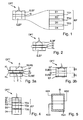
- the picture of the FIG. 1 shows a cross-sectional view of a first embodiment according to the invention of a stacked optocoupler device OPT together with an enlarged detail.
- the optocoupler module OPT comprises a transmitter module S with a transmitter area SF with a surface and a receiver module E with a receiver area EF and with a surface.
- the detail enlargement shows a basic structure of a reception area EF.
- the area size of the reception area EF and of the receiver module E is identical to the area size of the transmission area SF and the transmitter module S.
- the optocoupler module OPT comprises a plate-shaped electrical insulator IS, wherein the insulator IS is formed between the transmitter module S and the receiver module E.
- the isolator IS is transparent at least for the emission wavelengths of the transmitter module S.
- the three building blocks S, IS and E are arranged such that the gravity line of the surface of the transmission area SF and the gravity line of the surface of the reception area EF are exactly parallel to each other and the two gravity lines have no offset.
- the Light L of the transmitter module S acts directly on the receiver module E through the isolator IS.
- the receiver module E has a number of four partial voltage sources connected in series with each other.
- Each of the partial voltage sources comprises a semiconductor diode D1 to D4.
- the diodes D1 to D4 have a p-n junction, not shown.
- a tunnel diode TD1 to TD3 is arranged between each two successive partial voltage sources in each case.
- the partial voltage sources and the tunnel diodes TD1 to TD3 are integrated together monolithically.
- the receiver module E When irradiated by the transmitter module S, the receiver module E generates a total voltage above 2 V, wherein the individual diodes of the stack generate almost an identical partial voltage.
- FIG. 2 is a cross-sectional view of a second embodiment according to the invention an optocoupler device OPT shown.
- the surface of the plate-shaped insulator IS is larger than the surface of the transmitter module S and the surface of the receiver module E, so that the insulator IS protruding circumferentially balcony-like out of the stack.
- a transparent connection layer KL is formed in each case.
- FIG. 3a is a cross-sectional view of a third embodiment of an optocoupler device OPT invention shown.
- the transmitter module S comprises a substrate layer SUBS in addition to the transmitter area SF.
- the receiver module E comprises in addition to the receiver area EF a substrate layer SUBE. Both substrate layers SUBS and SUBE are formed as carrier layers. Between the two substrate layers SUBS and SUBE, the transmission range SF and the reception range EF are arranged. On the top and bottom of the plate-shaped insulator IS respectively the transparent connection layer KL is formed.
- the bonding layer KL is thinner than 0.2 mm, preferably thinner than 0.02 mm, and connects the upper side of the insulator to the transmitting region SF and the underside of the insulator in a materially bonded manner to the receiving region.
- the advantage of the arrangement is that the light L of the transmitting area SF strikes the receiving area EF directly through the isolator IS.
- FIG. 3b is a cross-sectional view of a fourth embodiment of the invention an optocoupler device OPT shown.
- the substrate layer SUBS is arranged between the transmitting region SF and the isolator IS, and the substrate layer SUBE is arranged between the receiving region EF and the isolator IS.
- the light L also passes through the two substrate layers SUBS and SUBE in order to be absorbed onto the reception area EF. It is understood that the substrate layers SUBS and SUBE have a low absorption in the region of the emission wavelength of the transmitter module S.
- Fig. 4 is a cross-sectional view is shown on a detailed representation of the receiver module E as part of the optocoupler module OPT.
- the layer thicknesses of the diodes D1 to D4 increase continuously with the distance of the respective diode from the insulator IS, the fourth diode D4 having the greatest layer thickness.
- FIG. 5 is a cross-sectional view of a packaged embodiment of an optocoupler device OPT shown.
- the stack of transmitter module S and isolator IS and receiver module E are integrated in a common housing G.
- the transmitter module S has a first electrical connection contact KS1 and a second electrical contact connection KS2.
- the receiver module E has a first electrical connection contact KE1 and a second electrical connection contact KE2.
Abstract
Stapelförmiger Optokopplerbaustein, aufweisend einen Senderbaustein (S) mit einem Sendebereich (SF), einen Empfängerbaustein (E) mit einem Empfangsbereich (EF) und einen plattenförmigen elektrischen Isolator (IS), wobei der Isolator zwischen dem Senderbaustein und dem Empfängerbaustein ausgebildet ist. Der Senderbaustein (S), der Empfängerbaustein (E) und der Isolator (IS) sind stapelförmig aufeinander angeordnet, wodurch der Senderbaustein und der Empfängerbaustein voneinander galvanisch getrennt jedoch miteinander optisch gekoppelt sind. Der Isolator (IS) ist für die Emissionswellenlängen des Senderbausteins (E) transparent. Eine Schwerelinie der Oberfläche des Sendebereichs und eine Schwerelinie der Oberfläche des Empfangsbereichs sind im Wesentlichen zueinander parallel, und der Versatz zwischen den beiden Schwerelinien ist kleiner als die Hälfte der Entfernung der jeweiligen Schwerelinien zu einer Außenkante des Sendebereichs oder zu einer Außenkante des Empfangsbereichs, so dass das Licht des Senderbausteins überwiegend durch den Isolator auf den Empfängerbaustein einwirkt. Der Empfängerbaustein (E) weist eine Anzahl N zueinander in Serie geschalteter Teilspannungsquellen auf, wobei N eine natürliche Zahl ist. Die Abweichungen der Teilspannungen der einzelnen Teilspannungsquellen untereinander sind kleiner als 20%. Jede der Teilspannungsquellen weist eine Halbleiterdiode (D1 - D4) mit einem p-n Übergang auf. Zwischen jeweils zwei aufeinanderfolgenden Teilspannungsquellen ist eine Tunneldiode (TD1-TD3) ausgebildet. Die Teilspannungsquellen und die Tunneldioden sind zusammen monolithisch integriert. Durch diese neuartige Anordnung lassen sich sehr kompakte und kleine Optokopplerbausteine herstellen, die eine hohe Schaltgeschwindigkeit aufweisen.Stack-shaped optocoupler module, comprising a transmitter module (S) with a transmitter area (SF), a receiver module (E) with a receiver area (EF) and a plate-shaped electrical insulator (IS), wherein the isolator is formed between the transmitter module and the receiver module. The transmitter module (S), the receiver module (E) and the isolator (IS) are stacked on top of each other, whereby the transmitter module and the receiver module are electrically isolated from each other but optically coupled. The isolator (IS) is transparent to the emission wavelengths of the transmitter module (E). A gravity line of the surface of the transmission area and a gravity line of the surface of the reception area are substantially parallel to each other, and the offset between the two gravity lines is smaller than half the distance of the respective gravity lines to an outside edge of the transmission area or to an outside edge of the reception area, so that the light of the transmitter module predominantly acts on the receiver module through the isolator. The receiver module (E) has a number N of partial voltage sources connected in series with each other, where N is a natural number. The deviations of the partial voltages of the individual partial voltage sources with one another are less than 20%. Each of the partial voltage sources has a semiconductor diode (D1-D4) with a p-n junction. Between each two successive partial voltage sources, a tunnel diode (TD1-TD3) is formed. The partial voltage sources and the tunnel diodes are monolithically integrated together. This novel arrangement makes it possible to produce very compact and small optocoupler devices which have a high switching speed.
Description
Die Erfindung betrifft einen stapelförmigen Optokopplerbaustein.The invention relates to a stacked optocoupler device.
Aus der
Vor diesem Hintergrund besteht die Aufgabe der Erfindung darin, eine Vorrichtung anzugeben, die den Stand der Technik weiterbildet.Against this background, the object of the invention is to provide a device which further develops the prior art.
Die Aufgabe wird durch einen stapelförmigen Optokopplerbaustein mit den Merkmalen des Patentanspruchs 1 gelöst. Vorteilhafte Ausgestaltungen der Erfindung sind Gegenstand von Unteransprüchen.The object is achieved by a stack-shaped optocoupler module having the features of patent claim 1. Advantageous embodiments of the invention are the subject of dependent claims.
Gemäß dem Gegenstand der Erfindung wird ein stapelförmiger Optokopplerbaustein bereitgestellt, aufweisend einen Senderbaustein mit einem Sendebereich, wobei der Sendebereich eine Oberfläche aufweist, und einen Empfängerbaustein mit einem Empfangsbereich, wobei der Empfangsbereich eine Oberfläche aufweist, und einen plattenförmigen elektrischen Isolator, wobei der Isolator zwischen dem Senderbaustein und dem Empfängerbaustein ausgebildet ist, und der Senderbaustein und der Empfängerbaustein und der Isolator stapelförmig aufeinander angeordnet sind und der Isolator eine Oberseite und eine Unterseite aufweist. Der Senderbaustein und der Empfängerbaustein sind galvanisch voneinander getrennt, jedoch miteinander optisch gekoppelt, wobei der Isolator wenigstens für ein Teil der Emissionswellenlängen des Senderbausteins transparent ist, und die Schwerelinie der Oberfläche des Sendebereichs und die Schwerelinie der Oberfläche des Empfangsbereichs im Wesentlichen oder exakt zueinander parallel sind, und der Versatz zwischen den beiden Schwerelinien kleiner als die Hälfte oder kleiner als ein Zehntel oder kleiner als ein fünfzigstel der Entfernung der jeweiligen Schwerelinien zu einer Außenkante der Oberfläche des Sendebereichs oder zu einer Außenkante der Oberfläche des Empfangsbereichs ist, so dass das Licht des Senderbausteins überwiegend oder ausschließlich durch den Isolator auf den Empfängerbaustein bzw. auf die Oberfläche des Empfangsbereichs und auf den Empfangsbereich einwirkt, und der Isolators auf allen Seiten aus dem Stapel balkonförmig um maximal 250 µm hervorsteht, und der Empfängerbaustein eine Anzahl N zueinander in Serie geschalteten Teilspannungsquellen aufweist, wobei N eine natürliche Zahl und N ≥ 2 ist, und die Abweichung der Teilspannungen der einzelnen Teilspannungsquellenuntereinander kleiner als 20% ist, und jede der Teilspannungsquellen eine Halbleiterdiode mit einen p-n Übergang aufweist, und zwischen jeweils zwei aufeinanderfolgenden Teilspannungsquellen eine Tunneldiode ausgebildet ist, wobei die Teilspannungsquellen und die Tunneldioden zusammen monolithisch integriert sind.According to the subject invention, there is provided a stacked optocoupler device comprising a transmitter module having a transmitter section, the transmitter section having a surface, and a receiver module having a receiver section, the receiver section having a surface, and a plate-shaped electrical insulator, wherein the isolator is disposed between the transmitter Transmitter module and the receiver module is formed, and the transmitter module and the receiver module and the insulator stacked are arranged on each other and the insulator has a top and a bottom. The transmitter module and the receiver module are galvanically separated from each other, but optically coupled to each other, wherein the insulator is transparent at least for a part of the emission wavelengths of the transmitter module, and the gravity line of the surface of the transmitter area and the gravity line of the surface of the receiving area are substantially or exactly parallel to each other , and the offset between the two centroid lines is less than or less than one-tenth or less than one fiftieth of the distance of the respective centroid lines to an outer edge of the surface of the transmit area or to an outer edge of the surface of the receive area, such that the light of the transmitter block predominantly or exclusively by the insulator acts on the receiver module or on the surface of the receiving area and on the receiving area, and the insulator on all sides of the stack in the form of a balcony protrudes by a maximum of 250 microns, and the receiver module has a number N to each other in series connected partial voltage sources , where N is a natural number and N ≥ 2, and the deviation of the partial voltages of the individual partial voltage sources together is less than 20%, and each of the partial voltage sources comprises a semiconductor diode with a pn junction, and between each two successive partial voltage sources, a tunnel diode is formed the partial voltage sources and the tunnel diodes are monolithically integrated together.
Es sei angemerkt, dass der Senderbaustein und der Empfängerbaustein in Form von sogenannten "Dies" vorliegen, d.h. als ungehäuste Bausteine. Ferner weist der Senderbaustein neben dem Sendebereich auch eine Rückseite und der Empfängerbaustein neben dem Empfangsbereich auch eine Rückseite auf. Insgesamt liegt vorzugsweise der gesamte Stapel als ungehäustes Bauteil vor. Des Weiteren sei angemerkt, dass die Anzahl N bevorzugt gleich vier ist.It should be noted that the transmitter module and the receiver module are in the form of so-called "dies", i. as unhoused building blocks. Furthermore, the transmitter module also has a rear side in addition to the transmitter area and the receiver module also has a rear side in addition to the reception area. Overall, preferably the entire stack is present as an unhoused component. It should also be noted that the number N is preferably equal to four.
Es versteht sich, dass mit dem Begriff transparent eine geringe Absorption zumindest im Bereich der Sendewellenlänge zu verstehen ist. Vorzugsweise ist die Absorption in Bezug auf die eingestrahlte Intensität kleiner als 20% oder kleiner als 10%, höchst vorzugsweise kleiner als 5%.It is understood that the term transparent means a low absorption at least in the range of the transmission wavelength. Preferably, the absorption with respect to the irradiated intensity is less than 20% or less than 10%, most preferably less than 5%.
Des Weiteren versteht sich, dass bei dem Empfängerbaustein, genauer gesagt bei dem Empfangsbereich die Halbleiterdioden untereinander eine im Wesentlich gleiche oder eine genau gleiche Abfolge von Halbleiterschichten mit identischen oder im Wesentlichen identischen Halbleitermaterialien aufweisen und durch die Serienschaltung der Diode die Gesamtspannung des Empfängerbausteins die Summe der Teilspannungen ist. Hierdurch lässt sich auf einfache Weise eine nahezu identische Teilspannung der jeweiligen Halbleiterdioden erzielen. Vorzugsweise weicht die Teilspannung weniger als 10 % zwischen beliebigen zwei Halbleiterdioden des Stapels voneinander ab. Ferner sei angemerkt, dass mit einem zunehmenden Abstand der einzelnen Diode von dem Isolator die Dicke des Absorptionsbereichs und hiermit die Gesamtdicke der einzelnen Diode stark, vorzugsweise exponentiell zunehmen.Furthermore, it is understood that in the receiver module, more precisely in the receiving region, the semiconductor diodes have a substantially identical or exactly the same sequence of semiconductor layers with identical or substantially identical semiconductor materials and by the series connection of the diode, the total voltage of the receiver module, the sum of Partial stresses is. As a result, a nearly identical partial voltage of the respective semiconductor diodes can be achieved in a simple manner. Preferably, the partial voltage deviates less than 10% between any two semiconductor diodes of the stack from each other. Further It should be noted that with an increasing distance of the individual diode from the insulator, the thickness of the absorption region and hereby the total thickness of the individual diode increase strongly, preferably exponentially.
Ein Vorteil ist, dass durch die neuartige stapelförmige Anordnung von mehreren monolithischen Dioden in dem Empfängerbaustein verbunden mit einer hohen Lichtempfindlichkeit sich sehr kompakte und kleine Optokopplerbausteine herstellen lassen. Insbesondere lässt sich eine direkte Einkopplung des emittierten Lichts erzielen, d.h. das Licht hat einen kurzen Weg durch den Isolator zurückzulegen, bevor das transmittierte Licht auf den Empfängerbaustein trifft.One advantage is that the novel stacked arrangement of a plurality of monolithic diodes in the receiver module combined with a high photosensitivity makes it possible to produce very compact and small optocoupler modules. In particular, a direct coupling of the emitted light can be achieved, i. the light has to travel a short distance through the isolator before the transmitted light hits the receiver module.
Ein weiterer Vorteil ist, dass der Empfängerbaustein neben einer hohen Spannung, vorzugsweise oberhalb 2 V, höchst vorzugsweise oberhalb von 4 V auch einen hohen Strom oberhalb von 1 mA / cm2, höchst vorzugsweise oberhalb von 100mA / cm2 zur Verfügung stellt. Hierdurch lassen sich hohe Schaltgeschwindigkeiten oberhalb 10 MHz, vorzugsweise oberhalb 100 MHz erzielen.A further advantage is that, in addition to a high voltage, preferably above 2 V, most preferably above 4 V, the receiver module also provides a high current above 1 mA / cm 2 , most preferably above 100mA / cm 2 . This makes it possible to achieve high switching speeds above 10 MHz, preferably above 100 MHz.
Des Weiteren sei angemerkt, dass es vorteilhaft ist, den Sendebereich unmittelbar mit der Oberseite des Isolators und den Empfangsbereich unmittelbar mit der Unterseite des Isolators zu verbinden, so dass der Sendebereich dem Empfangsbereich zugewandt ist. Hierdurch benötigt das emittierte Licht nur den minimalen Weg zu der Empfangsfläche, d.h. zu der Oberfläche des Empfangsbereichs.Furthermore, it should be noted that it is advantageous to connect the transmission area directly to the upper side of the isolator and the reception area directly to the underside of the isolator so that the transmission area faces the reception area. As a result, the emitted light requires only the minimum path to the receiving surface, i. to the surface of the reception area.
In einer alternativen Ausführung sind die Rückseite des Senderbausteins mit der Oberseite des Isolators und die Rückseite des Empfängerbausteins mit der Unterseite des Isolators verbunden. Untersuchungen haben gezeigt, dass bei Ausbildung einer Substratschicht an der Rückseite des Senderbausteins und eine Ausbildung einer Substratschicht an der Rückseite des Empfängerbausteins eine vorteilhafte stapelförmige Ausbildung gegeben ist, anders ausgedrückt die beiden Substratschichten sind vorliegend unmittelbar einander zugewandt. Mit der Ausbildung von den Substratschichten lässt sich die mechanische Stabilität des jeweiligen Bausteins erhöhen und eine zuverlässige Kontaktierung der Bausteine durchführen.In an alternative embodiment, the back of the transmitter module with the top of the insulator and the back of the receiver module are connected to the underside of the insulator. Investigations have shown that when a substrate layer is formed on the rear side of the transmitter module and a substrate layer is formed on the rear side of the receiver module, an advantageous stacked configuration is provided; in other words, the two substrate layers are directly facing each other. With the training of the substrate layers can be the increase mechanical stability of the respective block and perform a reliable contacting of the blocks.
In einer anderen Ausführungsform ist der Stapel aus Senderbaustein und Isolator und Empfängerbaustein in einem gemeinsamen Gehäuse integriert.In another embodiment, the stack of transmitter module and insulator and receiver module is integrated in a common housing.
In einer bevorzugten Weiterbildung weist der Empfängerbaustein und der Senderbaustein entlang der Stapelrichtung eine pyramidenstumpfartige Ausbildung auf, wobei der Unterschied in der Flächengröße zwischen der Unterseite des Pyramidenstumpfs und der Oberseite des Pyramidenstumpfs wenigstens 5 µm2 beträgt.In a preferred embodiment, the receiver module and the transmitter module along the stacking direction on a truncated pyramidal formation, wherein the difference in the area between the bottom of the truncated pyramid and the top of the truncated pyramid is at least 5 microns 2 .
In einer Weiterbildung ist der Unterschied zwischen der Größe der Oberfläche des Sendebereichs und der Größe der Oberfläche des Empfangsbereichs kleiner als 20%, vorzugsweise kleiner als 10%. Untersuchungen haben gezeigt, dass es vorteilhaft ist, die Oberfläche des Empfangsbereichs entweder gleich groß wie die Oberfläche des Sendebereichs auszuführen, oder alternativ die Oberfläche des Empfangsbereichs maximal 20 % größer als die Oberfläche des Sendebereichs auszuführen.In a development, the difference between the size of the surface of the transmission range and the size of the surface of the reception range is less than 20%, preferably less than 10%. Investigations have shown that it is advantageous to execute the surface of the receiving area either the same size as the surface of the transmitting area, or alternatively to carry out the surface of the receiving area at most 20% larger than the surface of the transmitting area.
Des Weiteren ist es bevorzugt, dass die gesamte Oberfläche des Sendebereichs und oder der Sendebereich Licht emittiert und die gesamte Oberfläche des Empfangsbereichs und der Empfangsbereich insgesamt Licht absorbiert. Hierdurch lässt sich der Wirkungsgrad des Optokopplerbausteins erhöhen. Es versteht sich, dass bei einer Emission des Lichts durch die Oberfläche des Sendebereichs eine möglichst geringe Fläche mit Kontaktmetall bedeckt ist. Nicht anders ergibt sich für den Fall der Absorption. Auch hier gilt bei einer Absorption des Lichtes durch die Oberfläche des Empfangsbereichs und in dem Empfangsbereich, dass eine möglichst geringe Fläche bzw. Flächenanteil an der gesamten Oberfläche des Empfangsbereichs mit Kontaktmetall bedeckt ist.Furthermore, it is preferable that the entire surface of the transmission region and / or the transmission region emit light, and the entire surface of the reception region and the reception region absorb light as a whole. As a result, the efficiency of the optocoupler module can be increased. It is understood that when the light is emitted through the surface of the transmitting region, the smallest possible area is covered with contact metal. The situation is different in the case of absorption. Here, too, when the light is absorbed by the surface of the receiving region and in the receiving region, the smallest possible area or area fraction on the entire surface of the receiving region is covered with contact metal.
In einer Ausführungsform weist die Oberfläche des Sendebereichs und die Oberfläche des Empfangsbereichs eine viereckige Form auf, wobei die größte Kantenlänge des jeweiligen Vierecks kleiner als 2 mm ist. In einer Weiterbildung sind die Oberflächen des Sendebereichs und die Oberfläche des Empfangsbereichs quadratisch ausgebildet und weisen jeweils eine Grundfläche größer als 0,2 x 0,2 mm2 und kleiner als 4 mm2 oder kleiner als 1 mm2 auf.In one embodiment, the surface of the transmit area and the surface of the receive area have a quadrangular shape, with the largest Edge length of the respective square is less than 2 mm. In a further development, the surfaces of the transmitting area and the surface of the receiving area are square and each have a base area greater than 0.2 x 0.2 mm 2 and less than 4 mm 2 or less than 1 mm 2 .
Des Weiteren ist es vorteilhaft, wenn die Oberflächen des Sendebereichs und die Oberfläche des Empfangsbereichs jeweils eine streifenförmige oder gitterförmige oder kleine Kontaktfläche mit einem Anteil von kleiner als 10% der gesamten Oberfläche oder eine ganzflächige Metallisierung aufweisen. Ferner weist die Rückseite des Senderbausteins als auch die Rückseite des Empfängerbausteins eine streifenförmige Kontaktfläche oder gitterförmige Kontaktfläche oder kleine Kontaktfläche mit einem Anteil von jeweils kleiner als 10% der gesamten Oberfläche oder eine ganzflächige Metallisierung auf.Furthermore, it is advantageous if the surfaces of the transmitting region and the surface of the receiving region each have a strip-shaped or lattice-shaped or small contact surface with a proportion of less than 10% of the entire surface or a whole-area metallization. Furthermore, the rear side of the transmitter module as well as the rear side of the receiver module have a strip-shaped contact surface or grid-shaped contact surface or small contact surface with a proportion of in each case less than 10% of the entire surface or a whole-area metallization.
In einer anderen Ausführungsform weist der Senderbaustein einen optischen Spiegel für die Wellenlänge des Senders oder eine RCLED oder einen oberflächenemittierenden Laser auf.In another embodiment, the transmitter module has an optical mirror for the wavelength of the transmitter or an RCLED or a surface-emitting laser.
Untersuchungen haben gezeigt, dass der plattenförmige Isolator vorzugsweise einen Kunststoff und / oder Glas und / oder Aluminiumdioxid und / oder Epoxidharz und / oder Silikon umfasst oder aus einer derartigen Verbindung besteht. Hierbei ist auch ein mehrschichtiger Aufbau aus verschieden Materialien umfasst. Insbesondere lassen sich beispielweise die beiden Bausteine, also Senderbaustein und der Empfängerbaustein jeweils mit einer dünnen als transparente Silikonklebeschicht ausgebildeten Verbindungsschicht kraftschlüssig mit einem dünnen Glasplättchen verbinden. Es versteht sich, dass sich der Senderbaustein und der Empfängerbaustein mit dem Isolator auch mittels anderen Verbindungsmaterialien und / oder Befestigungsmittel zu einem Stapel fügen lassen.Investigations have shown that the plate-shaped insulator preferably comprises or consists of a plastic and / or glass and / or aluminum dioxide and / or epoxy resin and / or silicone. This also includes a multi-layered construction of different materials. In particular, for example, the two building blocks, that is to say the transmitter building block and the receiver building block, can each be frictionally connected with a thin glass plate with a thin connecting layer formed as a transparent silicone adhesive layer. It is understood that the transmitter module and the receiver module with the insulator can also be added to a stack by means of other connection materials and / or fastening means.
In einer bevorzugten Weiterbildung ist die Dicke des Isolators kleiner als 0,5 mm, vorzugsweise kleiner als 0,3 mm, jedoch größer als 50µm. Es versteht sich hierbei, dass die Dicke des Isolators so gewählt ist, dass eine Durchschlagsfestigkeit zwischen dem Senderbaustein und dem Empfängerbaustein von größer als 2kV gewährleistet ist. Hierbei ist es vorteilhaft, wenn der plattenförmige Isolator auf allen Seiten aus dem Stapel um wenigstens 5 µm hervorsteht, d.h. der Isolator bildet einen umlaufenden Balkon aus.In a preferred development, the thickness of the insulator is less than 0.5 mm, preferably less than 0.3 mm, but greater than 50 .mu.m. It is understood here that the thickness of the insulator is selected such that a dielectric strength between the transmitter module and the receiver module is guaranteed by greater than 2kV. It is advantageous if the plate-shaped insulator protrudes on all sides of the stack by at least 5 microns, ie, the insulator forms a circumferential balcony.
In einer anderen Ausführungsform ist die Gesamtdicke des Stapels aus Senderbaustein und Isolator und Empfängerbaustein ungehäust kleiner als 3 mm, vorzugsweise kleiner als 2 mm, höchst vorzugsweise kleiner als 1,2 mm, jedoch dicker als 0,2 mm.In another embodiment, the total thickness of the stack of transmitter module and insulator and receiver module is unhoused less than 3 mm, preferably less than 2 mm, most preferably less than 1.2 mm, but thicker than 0.2 mm.
Zur Erhöhung des Kopplungswirkungsgrades zwischen dem Senderbaustein und dem Empfängerbaustein ist es vorteilhaft, dass die Emissionswellenlänge des Senderbausteins gleich oder um maximal 10 % kleiner als die Absorptionskante des Empfängerbausteins ist. In einer weiteren Ausbildung umfassen der Senderbaustein und der Empfängerbaustein ein III-V Material oder bestehen aus dem III-V Material. Insbesondere umfasst der Empfängerbaustein ein GaAs und / oder ein Ge-Substrat. Vorzugsweise umfasst der Empfängerbaustein ein (Al)GaAs und / oder ein InGaP und / oder ein InGaAs Material. Es sei angemerkt, dass ein in Klammer gesetztes Element, hier beispielsweise Aluminium, vorhanden sein kann, aber nicht vorhanden sein muss.To increase the coupling efficiency between the transmitter module and the receiver module, it is advantageous that the emission wavelength of the transmitter module is equal to or less than the absorption edge of the receiver module by at most 10%. In a further embodiment, the transmitter module and the receiver module comprise a III-V material or consist of the III-V material. In particular, the receiver module comprises a GaAs and / or a Ge substrate. The receiver module preferably comprises an (Al) GaAs and / or an InGaP and / or an InGaAs material. It should be noted that a stapled element, here aluminum, for example, may be present but need not be present.
Die Erfindung wird nachfolgend unter Bezugnahme auf die Zeichnungen näher erläutert. Hierbei werden gleichartige Teile mit identischen Bezeichnungen beschriftet. Die dargestellten Ausführungsformen sind stark schematisiert, d.h. die Abstände und die lateralen und die vertikalen Erstreckungen sind nicht maßstäblich und weisen, sofern nicht anders angegeben, auch keine ableitbaren geometrischen Relationen zueinander auf. Darin zeigt:
- Figur 1
- eine Querschnittsansicht auf eine erste erfindungsgemäße Ausführungsform mit einer Ausschnittsvergrößerung,
- Figur 2
- eine Querschnittsansicht auf eine zweite erfindungsgemäße Ausführungsform,
- Figur 3a
- eine Querschnittsansicht auf eine dritte erfindungsgemäße Ausführungsform mit einem Substrat,
- Figur 3b
- eine Querschnittsansicht auf eine vierte erfindungsgemäße Ausführungsform mit einem Substrat,
- Figur 4
- eine detaillierte Darstellung des Empfängerbausteins,
- Figur 5
- eine Querschnittsansicht auf eine gehäuste Ausführungsform.
- FIG. 1
- 3 shows a cross-sectional view of a first embodiment according to the invention with an enlarged detail,
- FIG. 2
- a cross-sectional view of a second embodiment of the invention,
- FIG. 3a
- a cross-sectional view of a third embodiment according to the invention with a substrate,
- FIG. 3b
- a cross-sectional view of a fourth embodiment according to the invention with a substrate,
- FIG. 4
- a detailed representation of the receiver module,
- FIG. 5
- a cross-sectional view of a packaged embodiment.
Die Abbildung der
Insgesamt ist der Senderbaustein S und der Empfängerbaustein E und der Isolator IS stapelförmig aufeinander angeordnet und miteinander kraftschlüssig verbunden, wobei der Senderbaustein S und der Empfängerbaustein E voneinander galvanisch getrennt jedoch miteinander optisch gekoppelt sind. Der Isolator IS ist zumindest für die Emissionswellenlängen des Senderbausteins S transparent. Die drei Bausteine S, IS und E sind derart angeordnet, dass die Schwerelinie der Oberfläche des Sendebereichs SF und die Schwerelinie der Oberfläche des Empfangsbereichs EF exakt zueinander parallel sind und die beiden Schwerelinien keinen Versatz aufweisen. Das Licht L des Senderbausteins S wirkt durch den Isolator IS unmittelbar auf den Empfängerbaustein E ein.Overall, the transmitter module S and the receiver module E and the insulator IS stacked arranged one another and positively connected to each other, the transmitter module S and the receiver module E are electrically isolated from each other, however, optically coupled. The isolator IS is transparent at least for the emission wavelengths of the transmitter module S. The three building blocks S, IS and E are arranged such that the gravity line of the surface of the transmission area SF and the gravity line of the surface of the reception area EF are exactly parallel to each other and the two gravity lines have no offset. The Light L of the transmitter module S acts directly on the receiver module E through the isolator IS.
In der Ausschnittsvergrößerung ist der Empfangsbereich EF des Empfängerbausteins E detailliert dargestellt. In einer elektrotechnischen Betrachtung weist der Empfängerbaustein E eine Anzahl von vier zueinander in Serie geschalteten Teilspannungsquellen auf. Jede der Teilspannungsquellen umfasst eine Halbleiterdiode D1 bis D4. Die Dioden D1 bis D4 weisen einen nicht dargestellten p-n Übergang auf. Zwischen jeweils zwei aufeinanderfolgenden Teilspannungsquellen ist jeweils eine Tunneldiode TD1 bis TD3 angeordnet. Die Teilspannungsquellen und die Tunneldioden TD1 bis TD3 sind zusammen monolithisch integriert. Bei einer Bestrahlung durch den Senderbaustein S erzeugt der Empfängerbaustein E eine Gesamtspannung oberhalb von 2 V, wobei die einzelnen Dioden des Stapels nahezu eine identische Teilspannung erzeugen.In the enlarged detail of the receiving area EF of the receiver module E is shown in detail. In an electrical analysis, the receiver module E has a number of four partial voltage sources connected in series with each other. Each of the partial voltage sources comprises a semiconductor diode D1 to D4. The diodes D1 to D4 have a p-n junction, not shown. Between each two successive partial voltage sources in each case a tunnel diode TD1 to TD3 is arranged. The partial voltage sources and the tunnel diodes TD1 to TD3 are integrated together monolithically. When irradiated by the transmitter module S, the receiver module E generates a total voltage above 2 V, wherein the individual diodes of the stack generate almost an identical partial voltage.
In der Abbildung der
In der Abbildung der
In der Abbildung der
In der Abbildung der
In der Abbildung der
Claims (17)
einen Empfängerbaustein (E) mit einem Empfangsbereich (EF), wobei der Empfangsbereich (EF) eine Oberfläche aufweist, und
der Isolator (IS) auf allen Seiten aus dem Stapel balkonförmig um maximal 250 µm hervorsteht, und
a receiver module (E) having a reception area (EF), the reception area (EF) having a surface, and
the insulator (IS) protrudes on all sides from the stack in the form of a balcony to a maximum of 250 μm, and
quadratisch sind und jeweils eine Grundfläche größer als 0,2 x 0,2 mm2 und kleiner als 4 mm2 oder kleiner als 1 mm2 aufweisen.Integrated optocoupler (OPK) according to one or more of the preceding claims, characterized in that the surface of the transmitting region (SF) and the surface of the receiving region (EF)
are square and each have a footprint greater than 0.2 x 0.2 mm 2 and less than 4 mm 2 or less than 1 mm 2 .
Priority Applications (6)
| Application Number | Priority Date | Filing Date | Title |
|---|---|---|---|
| EP15001126.0A EP3082169A1 (en) | 2015-04-17 | 2015-04-17 | Stacked optocoupler module |
| EP16000853.8A EP3082170B1 (en) | 2015-04-17 | 2016-04-15 | Stacked optocoupler module |
| TW105111902A TWI627762B (en) | 2015-04-17 | 2016-04-15 | Stacked optocoupler component |
| JP2016082164A JP6129377B2 (en) | 2015-04-17 | 2016-04-15 | Multilayer photocoupler module |
| CN201610243774.6A CN106057962B (en) | 2015-04-17 | 2016-04-18 | Stack the photo-coupler component of shape |
| US15/131,121 US10050169B2 (en) | 2015-04-17 | 2016-04-18 | Stacked optocoupler component |
Applications Claiming Priority (1)
| Application Number | Priority Date | Filing Date | Title |
|---|---|---|---|
| EP15001126.0A EP3082169A1 (en) | 2015-04-17 | 2015-04-17 | Stacked optocoupler module |
Publications (1)
| Publication Number | Publication Date |
|---|---|
| EP3082169A1 true EP3082169A1 (en) | 2016-10-19 |
Family
ID=52997172
Family Applications (2)
| Application Number | Title | Priority Date | Filing Date |
|---|---|---|---|
| EP15001126.0A Withdrawn EP3082169A1 (en) | 2015-04-17 | 2015-04-17 | Stacked optocoupler module |
| EP16000853.8A Active EP3082170B1 (en) | 2015-04-17 | 2016-04-15 | Stacked optocoupler module |
Family Applications After (1)
| Application Number | Title | Priority Date | Filing Date |
|---|---|---|---|
| EP16000853.8A Active EP3082170B1 (en) | 2015-04-17 | 2016-04-15 | Stacked optocoupler module |
Country Status (5)
| Country | Link |
|---|---|
| US (1) | US10050169B2 (en) |
| EP (2) | EP3082169A1 (en) |
| JP (1) | JP6129377B2 (en) |
| CN (1) | CN106057962B (en) |
| TW (1) | TWI627762B (en) |
Cited By (1)
| Publication number | Priority date | Publication date | Assignee | Title |
|---|---|---|---|---|
| WO2023046373A1 (en) * | 2021-09-23 | 2023-03-30 | Osram Opto Semiconductors Gmbh | Optoelectronic device |
Families Citing this family (5)
| Publication number | Priority date | Publication date | Assignee | Title |
|---|---|---|---|---|
| DE102017004149A1 (en) * | 2017-05-02 | 2018-11-08 | Azur Space Solar Power Gmbh | Light-receiving unit |
| EP3470872B1 (en) * | 2017-10-11 | 2021-09-08 | Melexis Technologies NV | Sensor device |
| DE102017011643B4 (en) * | 2017-12-15 | 2020-05-14 | Azur Space Solar Power Gmbh | Optical voltage source |
| US11322542B2 (en) * | 2020-03-27 | 2022-05-03 | Harvatek Corporation | Light-emitting diode (LED) assembly and method of manufacturing an LED cell of the same |
| US11658257B2 (en) * | 2020-03-27 | 2023-05-23 | Harvatek Corporation | Light source assembly, optical sensor assembly, and method of manufacturing a cell of the same |
Citations (14)
| Publication number | Priority date | Publication date | Assignee | Title |
|---|---|---|---|---|
| US4127862A (en) | 1977-09-06 | 1978-11-28 | Bell Telephone Laboratories, Incorporated | Integrated optical detectors |
| JPS587886A (en) * | 1981-07-07 | 1983-01-17 | Oki Electric Ind Co Ltd | Manufacture of semiconductor device |
| DE3317054A1 (en) | 1983-05-10 | 1984-11-15 | Licentia Patent-Verwaltungs-Gmbh, 6000 Frankfurt | Optocoupler |
| DE3633181A1 (en) | 1986-09-30 | 1988-04-07 | Siemens Ag | METHOD FOR PRODUCING AN OPTO COUPLER OR A REFLECTIVE LIGHT BARRIER AND RELATED OPTOCOUPLER OR RELATED REFLECTIVE BARRIER |
| US4766471A (en) * | 1986-01-23 | 1988-08-23 | Energy Conversion Devices, Inc. | Thin film electro-optical devices |
| US4996577A (en) | 1984-01-23 | 1991-02-26 | International Rectifier Corporation | Photovoltaic isolator and process of manufacture thereof |
| DE10011258A1 (en) | 2000-03-08 | 2001-09-20 | Rossendorf Forschzent | Integrated optocoupler and process for its manufacture |
| US20060048811A1 (en) * | 2004-09-09 | 2006-03-09 | Krut Dimitri D | Multijunction laser power converter |
| US20060060955A1 (en) | 2004-09-22 | 2006-03-23 | Texas Instruments Incorporated | Stacked die infrared transceiver bus |
| JP3816114B2 (en) * | 1993-01-18 | 2006-08-30 | シャープ株式会社 | Optical coupling device |
| US20080173879A1 (en) * | 2007-01-24 | 2008-07-24 | Stmicroelectronics S.R.L. | Galvanic optocoupler and method of making |
| US20140042344A1 (en) | 2012-08-08 | 2014-02-13 | Avago Technologies General Ip (Singapore) Pte. Ltd | Face-to-face optocoupler device and method of manufacture |
| US20140212085A1 (en) | 2013-01-29 | 2014-07-31 | Georgios Margaritis | Optocoupler |
| JP2015029037A (en) * | 2013-06-25 | 2015-02-12 | パナソニックIpマネジメント株式会社 | Optical coupling semiconductor device |
Family Cites Families (14)
| Publication number | Priority date | Publication date | Assignee | Title |
|---|---|---|---|---|
| JPS5893267A (en) * | 1981-11-30 | 1983-06-02 | Toshiba Corp | Photocoupling integrated circuit |
| JPS62244181A (en) * | 1986-04-17 | 1987-10-24 | Nec Corp | Photocoupler |
| JPS6344776A (en) * | 1986-08-12 | 1988-02-25 | Res Dev Corp Of Japan | Semiconductor device using quantum well |
| DE4005835C2 (en) * | 1989-02-23 | 1996-10-10 | Agency Ind Science Techn | Method for operating a photoelectric converter and photoelectric converter for carrying out the method |
| JPH0368177A (en) * | 1989-08-07 | 1991-03-25 | Sharp Corp | Thin film photocoupler |
| DD287356A5 (en) * | 1989-08-23 | 1991-02-21 | Veb Werk Fuer Fernsehelektronik,De | HIGH VOLTAGE-RESISTANT OPTOCOUPLER |
| JPH0645636A (en) * | 1992-07-24 | 1994-02-18 | Sharp Corp | Photodetection and light-emitting element and photodetection and light-emitting device utilizing it |
| DE19638194A1 (en) * | 1996-09-19 | 1998-04-02 | Telefunken Microelectron | Coupler manufacturing method |
| JP3874145B2 (en) | 1998-06-10 | 2007-01-31 | ソニー株式会社 | Modulation circuit, transmission device, and transmission circuit |
| US6787693B2 (en) * | 2001-12-06 | 2004-09-07 | International Rectifier Corporation | Fast turn on/off photovoltaic generator for photovoltaic relay |
| US8134172B2 (en) * | 2003-09-01 | 2012-03-13 | Lg Innotek Co., Ltd. | LED and fabrication method thereof |
| US20060004818A1 (en) | 2004-07-01 | 2006-01-05 | Claudatos Christopher H | Efficient information management |
| US20140036343A1 (en) * | 2012-07-31 | 2014-02-06 | Qualcomm Mems Technologies, Inc. | Interferometric modulator with improved primary colors |
| JP5865859B2 (en) * | 2013-03-22 | 2016-02-17 | 株式会社東芝 | Optical coupling device |
-
2015
- 2015-04-17 EP EP15001126.0A patent/EP3082169A1/en not_active Withdrawn
-
2016
- 2016-04-15 TW TW105111902A patent/TWI627762B/en active
- 2016-04-15 EP EP16000853.8A patent/EP3082170B1/en active Active
- 2016-04-15 JP JP2016082164A patent/JP6129377B2/en active Active
- 2016-04-18 CN CN201610243774.6A patent/CN106057962B/en active Active
- 2016-04-18 US US15/131,121 patent/US10050169B2/en active Active
Patent Citations (14)
| Publication number | Priority date | Publication date | Assignee | Title |
|---|---|---|---|---|
| US4127862A (en) | 1977-09-06 | 1978-11-28 | Bell Telephone Laboratories, Incorporated | Integrated optical detectors |
| JPS587886A (en) * | 1981-07-07 | 1983-01-17 | Oki Electric Ind Co Ltd | Manufacture of semiconductor device |
| DE3317054A1 (en) | 1983-05-10 | 1984-11-15 | Licentia Patent-Verwaltungs-Gmbh, 6000 Frankfurt | Optocoupler |
| US4996577A (en) | 1984-01-23 | 1991-02-26 | International Rectifier Corporation | Photovoltaic isolator and process of manufacture thereof |
| US4766471A (en) * | 1986-01-23 | 1988-08-23 | Energy Conversion Devices, Inc. | Thin film electro-optical devices |
| DE3633181A1 (en) | 1986-09-30 | 1988-04-07 | Siemens Ag | METHOD FOR PRODUCING AN OPTO COUPLER OR A REFLECTIVE LIGHT BARRIER AND RELATED OPTOCOUPLER OR RELATED REFLECTIVE BARRIER |
| JP3816114B2 (en) * | 1993-01-18 | 2006-08-30 | シャープ株式会社 | Optical coupling device |
| DE10011258A1 (en) | 2000-03-08 | 2001-09-20 | Rossendorf Forschzent | Integrated optocoupler and process for its manufacture |
| US20060048811A1 (en) * | 2004-09-09 | 2006-03-09 | Krut Dimitri D | Multijunction laser power converter |
| US20060060955A1 (en) | 2004-09-22 | 2006-03-23 | Texas Instruments Incorporated | Stacked die infrared transceiver bus |
| US20080173879A1 (en) * | 2007-01-24 | 2008-07-24 | Stmicroelectronics S.R.L. | Galvanic optocoupler and method of making |
| US20140042344A1 (en) | 2012-08-08 | 2014-02-13 | Avago Technologies General Ip (Singapore) Pte. Ltd | Face-to-face optocoupler device and method of manufacture |
| US20140212085A1 (en) | 2013-01-29 | 2014-07-31 | Georgios Margaritis | Optocoupler |
| JP2015029037A (en) * | 2013-06-25 | 2015-02-12 | パナソニックIpマネジメント株式会社 | Optical coupling semiconductor device |
Cited By (1)
| Publication number | Priority date | Publication date | Assignee | Title |
|---|---|---|---|---|
| WO2023046373A1 (en) * | 2021-09-23 | 2023-03-30 | Osram Opto Semiconductors Gmbh | Optoelectronic device |
Also Published As
| Publication number | Publication date |
|---|---|
| TWI627762B (en) | 2018-06-21 |
| US20160308085A1 (en) | 2016-10-20 |
| CN106057962A (en) | 2016-10-26 |
| EP3082170B1 (en) | 2021-02-17 |
| JP2016208028A (en) | 2016-12-08 |
| TW201703271A (en) | 2017-01-16 |
| EP3082170A2 (en) | 2016-10-19 |
| EP3082170A3 (en) | 2016-11-09 |
| CN106057962B (en) | 2017-12-26 |
| US10050169B2 (en) | 2018-08-14 |
| JP6129377B2 (en) | 2017-05-17 |
Similar Documents
| Publication | Publication Date | Title |
|---|---|---|
| EP3082169A1 (en) | Stacked optocoupler module | |
| EP0731509A1 (en) | Optoelectronic converter and process of manufacturing | |
| DE3390103C2 (en) | ||
| DE69927447T2 (en) | Device with an optical function and special connection electrodes | |
| EP0645827B1 (en) | Optocoupler and process of manufacturing the same | |
| DE19640423C1 (en) | Optoelectronic module for bidirectional optical data transmission | |
| DE102011113483B4 (en) | Method for producing a plurality of optoelectronic components and optoelectronic component | |
| DE102013214896B4 (en) | Method for producing a converter element and an optoelectronic component, converter element and optoelectronic component | |
| DE3633181A1 (en) | METHOD FOR PRODUCING AN OPTO COUPLER OR A REFLECTIVE LIGHT BARRIER AND RELATED OPTOCOUPLER OR RELATED REFLECTIVE BARRIER | |
| EP0335104A2 (en) | Arrangement to optically couple one or a plurality of optical senders to one or a plurality of optical receivers of one or a plurality of integrated circuits | |
| WO2020169524A1 (en) | Optoelectronic semiconductor component, and method for producing optoelectronic semiconductor components | |
| DE102017111706A1 (en) | Light emitting device | |
| DE60223783T2 (en) | Method for producing optoelectronic components for optical parallel connections | |
| WO2017072294A1 (en) | Optoelectronic component and method for producing same | |
| EP0929836B1 (en) | Method for producing a beam-splitting shaped body and use of the beam-splitting shaped body in an opto-electronic module | |
| WO2016113248A1 (en) | Optoelectronic component | |
| DE19640421A1 (en) | Optoelectronic module for bidirectional optical data transmission | |
| EP0053742A1 (en) | Method of transmitting signals, semiconductor device and electro-optical device for carrying out this method | |
| DE10022713A1 (en) | Optical unit dispersing e.g. light from LEDs used in traffic lights, includes extended raised sections along light disperser | |
| DE2330785A1 (en) | PHOTODETECTOR EQUALIZER | |
| WO2016071439A1 (en) | Method for producing an optoelectronic component, and optoelectronic component | |
| WO2016041784A1 (en) | Optoelectronic component | |
| DE19810624A1 (en) | Electro-optical module | |
| DE102018214803B4 (en) | Device for coupling electromagnetic waves into a chip | |
| EP2983214B1 (en) | Optocoupler |
Legal Events
| Date | Code | Title | Description |
|---|---|---|---|
| PUAI | Public reference made under article 153(3) epc to a published international application that has entered the european phase |
Free format text: ORIGINAL CODE: 0009012 |
|
| AK | Designated contracting states |
Kind code of ref document: A1 Designated state(s): AL AT BE BG CH CY CZ DE DK EE ES FI FR GB GR HR HU IE IS IT LI LT LU LV MC MK MT NL NO PL PT RO RS SE SI SK SM TR |
|
| AX | Request for extension of the european patent |
Extension state: BA ME |
|
| STAA | Information on the status of an ep patent application or granted ep patent |
Free format text: STATUS: THE APPLICATION HAS BEEN WITHDRAWN |
|
| 18W | Application withdrawn |
Effective date: 20161027 |