EP0731374A1 - Flüssigkristallanzeige mit verbessertem Sichtwinkel - Google Patents
Flüssigkristallanzeige mit verbessertem Sichtwinkel Download PDFInfo
- Publication number
- EP0731374A1 EP0731374A1 EP96400396A EP96400396A EP0731374A1 EP 0731374 A1 EP0731374 A1 EP 0731374A1 EP 96400396 A EP96400396 A EP 96400396A EP 96400396 A EP96400396 A EP 96400396A EP 0731374 A1 EP0731374 A1 EP 0731374A1
- Authority
- EP
- European Patent Office
- Prior art keywords
- liquid crystal
- cell according
- electric field
- pixel
- counter electrode
- Prior art date
- Legal status (The legal status is an assumption and is not a legal conclusion. Google has not performed a legal analysis and makes no representation as to the accuracy of the status listed.)
- Granted
Links
Images

Classifications
-
- G—PHYSICS
- G02—OPTICS
- G02F—OPTICAL DEVICES OR ARRANGEMENTS FOR THE CONTROL OF LIGHT BY MODIFICATION OF THE OPTICAL PROPERTIES OF THE MEDIA OF THE ELEMENTS INVOLVED THEREIN; NON-LINEAR OPTICS; FREQUENCY-CHANGING OF LIGHT; OPTICAL LOGIC ELEMENTS; OPTICAL ANALOGUE/DIGITAL CONVERTERS
- G02F1/00—Devices or arrangements for the control of the intensity, colour, phase, polarisation or direction of light arriving from an independent light source, e.g. switching, gating or modulating; Non-linear optics
- G02F1/01—Devices or arrangements for the control of the intensity, colour, phase, polarisation or direction of light arriving from an independent light source, e.g. switching, gating or modulating; Non-linear optics for the control of the intensity, phase, polarisation or colour
- G02F1/13—Devices or arrangements for the control of the intensity, colour, phase, polarisation or direction of light arriving from an independent light source, e.g. switching, gating or modulating; Non-linear optics for the control of the intensity, phase, polarisation or colour based on liquid crystals, e.g. single liquid crystal display cells
- G02F1/133—Constructional arrangements; Operation of liquid crystal cells; Circuit arrangements
- G02F1/1333—Constructional arrangements; Manufacturing methods
- G02F1/1337—Surface-induced orientation of the liquid crystal molecules, e.g. by alignment layers
- G02F1/133753—Surface-induced orientation of the liquid crystal molecules, e.g. by alignment layers with different alignment orientations or pretilt angles on a same surface, e.g. for grey scale or improved viewing angle
-
- G—PHYSICS
- G02—OPTICS
- G02F—OPTICAL DEVICES OR ARRANGEMENTS FOR THE CONTROL OF LIGHT BY MODIFICATION OF THE OPTICAL PROPERTIES OF THE MEDIA OF THE ELEMENTS INVOLVED THEREIN; NON-LINEAR OPTICS; FREQUENCY-CHANGING OF LIGHT; OPTICAL LOGIC ELEMENTS; OPTICAL ANALOGUE/DIGITAL CONVERTERS
- G02F1/00—Devices or arrangements for the control of the intensity, colour, phase, polarisation or direction of light arriving from an independent light source, e.g. switching, gating or modulating; Non-linear optics
- G02F1/01—Devices or arrangements for the control of the intensity, colour, phase, polarisation or direction of light arriving from an independent light source, e.g. switching, gating or modulating; Non-linear optics for the control of the intensity, phase, polarisation or colour
- G02F1/13—Devices or arrangements for the control of the intensity, colour, phase, polarisation or direction of light arriving from an independent light source, e.g. switching, gating or modulating; Non-linear optics for the control of the intensity, phase, polarisation or colour based on liquid crystals, e.g. single liquid crystal display cells
- G02F1/133—Constructional arrangements; Operation of liquid crystal cells; Circuit arrangements
- G02F1/1333—Constructional arrangements; Manufacturing methods
- G02F1/1343—Electrodes
- G02F1/134309—Electrodes characterised by their geometrical arrangement
- G02F1/134336—Matrix
-
- G—PHYSICS
- G02—OPTICS
- G02F—OPTICAL DEVICES OR ARRANGEMENTS FOR THE CONTROL OF LIGHT BY MODIFICATION OF THE OPTICAL PROPERTIES OF THE MEDIA OF THE ELEMENTS INVOLVED THEREIN; NON-LINEAR OPTICS; FREQUENCY-CHANGING OF LIGHT; OPTICAL LOGIC ELEMENTS; OPTICAL ANALOGUE/DIGITAL CONVERTERS
- G02F1/00—Devices or arrangements for the control of the intensity, colour, phase, polarisation or direction of light arriving from an independent light source, e.g. switching, gating or modulating; Non-linear optics
- G02F1/01—Devices or arrangements for the control of the intensity, colour, phase, polarisation or direction of light arriving from an independent light source, e.g. switching, gating or modulating; Non-linear optics for the control of the intensity, phase, polarisation or colour
- G02F1/13—Devices or arrangements for the control of the intensity, colour, phase, polarisation or direction of light arriving from an independent light source, e.g. switching, gating or modulating; Non-linear optics for the control of the intensity, phase, polarisation or colour based on liquid crystals, e.g. single liquid crystal display cells
- G02F1/133—Constructional arrangements; Operation of liquid crystal cells; Circuit arrangements
- G02F1/1333—Constructional arrangements; Manufacturing methods
- G02F1/1335—Structural association of cells with optical devices, e.g. polarisers or reflectors
- G02F1/133509—Filters, e.g. light shielding masks
- G02F1/133512—Light shielding layers, e.g. black matrix
-
- G—PHYSICS
- G02—OPTICS
- G02F—OPTICAL DEVICES OR ARRANGEMENTS FOR THE CONTROL OF LIGHT BY MODIFICATION OF THE OPTICAL PROPERTIES OF THE MEDIA OF THE ELEMENTS INVOLVED THEREIN; NON-LINEAR OPTICS; FREQUENCY-CHANGING OF LIGHT; OPTICAL LOGIC ELEMENTS; OPTICAL ANALOGUE/DIGITAL CONVERTERS
- G02F1/00—Devices or arrangements for the control of the intensity, colour, phase, polarisation or direction of light arriving from an independent light source, e.g. switching, gating or modulating; Non-linear optics
- G02F1/01—Devices or arrangements for the control of the intensity, colour, phase, polarisation or direction of light arriving from an independent light source, e.g. switching, gating or modulating; Non-linear optics for the control of the intensity, phase, polarisation or colour
- G02F1/13—Devices or arrangements for the control of the intensity, colour, phase, polarisation or direction of light arriving from an independent light source, e.g. switching, gating or modulating; Non-linear optics for the control of the intensity, phase, polarisation or colour based on liquid crystals, e.g. single liquid crystal display cells
- G02F1/133—Constructional arrangements; Operation of liquid crystal cells; Circuit arrangements
- G02F1/1333—Constructional arrangements; Manufacturing methods
- G02F1/1337—Surface-induced orientation of the liquid crystal molecules, e.g. by alignment layers
- G02F1/133707—Structures for producing distorted electric fields, e.g. bumps, protrusions, recesses, slits in pixel electrodes
-
- G—PHYSICS
- G02—OPTICS
- G02F—OPTICAL DEVICES OR ARRANGEMENTS FOR THE CONTROL OF LIGHT BY MODIFICATION OF THE OPTICAL PROPERTIES OF THE MEDIA OF THE ELEMENTS INVOLVED THEREIN; NON-LINEAR OPTICS; FREQUENCY-CHANGING OF LIGHT; OPTICAL LOGIC ELEMENTS; OPTICAL ANALOGUE/DIGITAL CONVERTERS
- G02F1/00—Devices or arrangements for the control of the intensity, colour, phase, polarisation or direction of light arriving from an independent light source, e.g. switching, gating or modulating; Non-linear optics
- G02F1/01—Devices or arrangements for the control of the intensity, colour, phase, polarisation or direction of light arriving from an independent light source, e.g. switching, gating or modulating; Non-linear optics for the control of the intensity, phase, polarisation or colour
- G02F1/13—Devices or arrangements for the control of the intensity, colour, phase, polarisation or direction of light arriving from an independent light source, e.g. switching, gating or modulating; Non-linear optics for the control of the intensity, phase, polarisation or colour based on liquid crystals, e.g. single liquid crystal display cells
- G02F1/133—Constructional arrangements; Operation of liquid crystal cells; Circuit arrangements
- G02F1/1333—Constructional arrangements; Manufacturing methods
- G02F1/1343—Electrodes
- G02F1/134309—Electrodes characterised by their geometrical arrangement
- G02F1/134345—Subdivided pixels, e.g. for grey scale or redundancy
-
- G—PHYSICS
- G02—OPTICS
- G02F—OPTICAL DEVICES OR ARRANGEMENTS FOR THE CONTROL OF LIGHT BY MODIFICATION OF THE OPTICAL PROPERTIES OF THE MEDIA OF THE ELEMENTS INVOLVED THEREIN; NON-LINEAR OPTICS; FREQUENCY-CHANGING OF LIGHT; OPTICAL LOGIC ELEMENTS; OPTICAL ANALOGUE/DIGITAL CONVERTERS
- G02F1/00—Devices or arrangements for the control of the intensity, colour, phase, polarisation or direction of light arriving from an independent light source, e.g. switching, gating or modulating; Non-linear optics
- G02F1/01—Devices or arrangements for the control of the intensity, colour, phase, polarisation or direction of light arriving from an independent light source, e.g. switching, gating or modulating; Non-linear optics for the control of the intensity, phase, polarisation or colour
- G02F1/13—Devices or arrangements for the control of the intensity, colour, phase, polarisation or direction of light arriving from an independent light source, e.g. switching, gating or modulating; Non-linear optics for the control of the intensity, phase, polarisation or colour based on liquid crystals, e.g. single liquid crystal display cells
- G02F1/133—Constructional arrangements; Operation of liquid crystal cells; Circuit arrangements
- G02F1/136—Liquid crystal cells structurally associated with a semi-conducting layer or substrate, e.g. cells forming part of an integrated circuit
- G02F1/1362—Active matrix addressed cells
- G02F1/136213—Storage capacitors associated with the pixel electrode
Definitions
- the present invention relates to a particular electrooptical cell (or pixel) structure of liquid crystal screens allowing an improvement in the angular characteristic compared to known liquid crystal screens.
- Direct vision or projection liquid crystal screens are generally composed of lines (selection lines) and columns (data lines) at the intersections of which are located the pixel electrodes connected through transistors to these lines.
- the gates of these transistors form the selection lines and are controlled by peripheral control circuits which scan the lines and make the transistors of each line pass by, by means of the data lines connected to the other peripheral control circuits, to polarize the electrodes and modify the optical properties of the liquid crystal between these electrodes and the counter electrode (or reference electrode), thus allowing the formation of images on the screen.
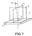
- FIG. 1 a twisted nematic liquid crystal cell 1 with two vision planes, the horizontal plane 2 and the vertical plane 3.
- a voltage across the electrodes creates an electric field across the liquid crystal straightening the direction of the molecules, and the pixel is in the non-conducting state, ie black.
- the angular distribution of the transmittance of light is symmetrical in the horizontal plane 2, and asymmetrical in the vertical plane 3.
- the direction of maximum contrast D corresponding to the minimum transmittance, is located in the vertical plane 3, its orientation depending on the voltage applied between the electrodes of the pixel, ie the brightness.
- the image displayed by the screen degrades as a function of the viewing angle at which it is perceived, this being able to go as far as an inversion of contrast for large angles.
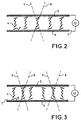
- FIG. 2 represents the alignment of these molecules 4 in the case of a nematic liquid crystal twisted in the presence of a voltage U between the electrodes 5 and 6.
- a alignment layer 7 which may be polyimide
- the directions of the dark 8 and light 9 zones mentioned above are given by the inclination that the molecules take in the presence of the electric field.
- the problem with this solution is its difficult technological realization, requiring etching of two different layers of alignment of the liquid crystal molecules, which appears extremely difficult to achieve in mass production.
- the present invention overcomes these drawbacks thanks to a screen structure which is very simple to produce.
- the present invention relates to an electrooptical cell (pixel) formed of two substrate plates comprising one, a pixel electrode and the other, a counter electrode between which liquid crystal molecules are included, in which the counter electrode is divided into two parts (or domains) by a groove, this groove preferably cutting the pixel in the middle, characterized in that a non-zero bias voltage is applied between the electrode and the counter-electrode when the pixel is not addressed.
- this voltage is between 0.8 and 1.3 times the value of the threshold polarization voltage of the liquid crystal in the presence of a homogeneous electric field.
- said cell has alignment layers of homogeneous liquid crystal molecules, the division of each pixel into two domains made up of molecules having different inclinations being only caused by the effect of the electric field between said electrode pixel and said counter electrode.
- said alignment layer can impose on the molecules of the liquid crystal either, an alignment strictly parallel to the stratum, or, in the presence of a intrinsic pre-tilt of said alignment layer, an anti-parallel alignment.
- Another improvement of the present invention consists in slightly increasing the thickness of the liquid crystal so as to maintain the optical characteristic in the presence of said bias voltage when the pixel is not addressed.
- this thickness is such that its product with birefringence, divided by the wavelength of light, is slightly greater than the constant ⁇ 3/2, typically between 1.1 and 1.5 times this constant.
- Another characteristic of the present invention is that an opaque material is deposited on one of the substrate plates in order to mask the groove of the counter electrode, this opaque material being able to be used as storage capacity.
- the present invention also relates to a liquid crystal screen comprising such electrooptical cells.
- the alignment layers 7 can be treated so as to obtain liquid crystal molecules 4, the alignment of which is said to be parallel, that is to say that they have a pre-inclination of 0 °. .
- This can be achieved by light brushing or printing the polyimide, or by oblique deposition of silicon oxide SiO.
- it is possible to use a so-called antiparallel alignment by using an alignment layer creating a pre-tilt other than zero. In this case, the layers at the top and bottom of the cell are arranged so that the two pre-slopes are opposite and cancel each other out. This type of alignment is called anti-parallel alignment.
- FIG. 5 is shown the section of a liquid crystal screen usable in the invention. It consists of two transparent substrate plates 11 on the inner surfaces of which are deposited transparent electrodes 14 and a transparent counter electrode 15. On the inner faces of these electrodes 14 and 15 are deposited and treated alignment layers 13. These layers can be either of the type allowing parallel alignment, or of the type imposing a pre-tilt of the liquid crystal molecules 4 located between these two layers. In the latter case, said layers at the top and bottom of the cell are arranged in an anti-parallel manner. Said liquid crystal can be twisted nematic or of any other type whose electrooptic effects are modified by an electric field E. Furthermore, these pixels are surrounded by two polarizers 7.
- the counter electrode 15 has a groove 18 cutting the pixel in the middle.
- this groove has a width of 0.5 to 2 times the thickness of the layer of the liquid crystal molecules 4, which is typically between 3 and 10 ⁇ m.
- a potential difference U is applied to the pixel electrodes 14 and to the counter electrode 15, this groove creates a component lateral to the electric field E.
- the electric field E is then perpendicular to the electrodes in the areas where they are made face, and oblique in the areas at the edges of the pixel electrodes 14 and in the areas between the groove 18 and the electrode 14, as indicated in FIG. 5.
- two optical domains each having different tilt directions are created by the non-homogeneous distribution of the electric field E due to the pixel structure according to the invention.
- an opaque material 16 for example on the outer face of the electrode 14.
- This material can be metal and can be used as storage capacity, for example in the case of addressing of active matrix.
- the counter electrode In the case of a screen addressed by an active matrix, the counter electrode generally covers the entire screen. In this case, it is necessary to etch this counter electrode in order to produce the grooves 18 in a very simple additional step.
- the mask used for this step can be the same as that used to deposit the opaque mask 16.
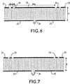
- FIG. 6 represents a sectional view of a liquid crystal screen according to a first embodiment of the invention. It is formed by electrodes 21, 22 and 23 separated by selection (or data) lines 24, and by a counter electrode 25 provided with grooves 26.
- the liquid crystal molecules 4 have a parallel alignment as described on the Figure 4a.
- Figure 7 shows a screen structure identical to that of the previous figure but with a pre-tilt of 1 °, the liquid crystal molecules have an anti-parallel alignment as described in Figure 4b.
- the polarization is not equal to zero when the pixel is not addressed (OFF state), so as to maintain the structure of the domains.
- the value of the bias voltage U is between 0.8 and 1.3 times the value of the threshold voltage of the liquid crystal in the presence of a homogeneous field.
- ⁇ n the birefringence
- ⁇ the wavelength of light.
- the present invention applies to all types of liquid crystal screens, direct vision or projection, provided with integrated or non-integrated control circuits.
Applications Claiming Priority (2)
| Application Number | Priority Date | Filing Date | Title |
|---|---|---|---|
| FR9502776 | 1995-03-09 | ||
| FR9502776A FR2731526B1 (fr) | 1995-03-09 | 1995-03-09 | Ecran a cristaux liquides a angle de vue ameliore |
Publications (2)
| Publication Number | Publication Date |
|---|---|
| EP0731374A1 true EP0731374A1 (de) | 1996-09-11 |
| EP0731374B1 EP0731374B1 (de) | 2010-04-14 |
Family
ID=9476908
Family Applications (1)
| Application Number | Title | Priority Date | Filing Date |
|---|---|---|---|
| EP96400396A Expired - Lifetime EP0731374B1 (de) | 1995-03-09 | 1996-02-26 | Flüssigkristallanzeige mit verbessertem Sichtwinkel |
Country Status (5)
| Country | Link |
|---|---|
| US (1) | US6327014B1 (de) |
| EP (1) | EP0731374B1 (de) |
| JP (1) | JPH08292414A (de) |
| DE (1) | DE69638160D1 (de) |
| FR (1) | FR2731526B1 (de) |
Cited By (1)
| Publication number | Priority date | Publication date | Assignee | Title |
|---|---|---|---|---|
| EP1734400A1 (de) * | 1998-11-27 | 2006-12-20 | SANYO ELECTRIC Co., Ltd. | Flüssigkristallanzeigevorrichtung |
Families Citing this family (5)
| Publication number | Priority date | Publication date | Assignee | Title |
|---|---|---|---|---|
| JP3966614B2 (ja) * | 1997-05-29 | 2007-08-29 | 三星電子株式会社 | 広視野角液晶表示装置 |
| US8913000B2 (en) * | 2007-06-15 | 2014-12-16 | Ricoh Co., Ltd. | Video playback on electronic paper displays |
| CN102736325B (zh) * | 2011-03-31 | 2015-08-12 | 京东方科技集团股份有限公司 | 一种像素结构及其制造方法、显示装置 |
| CN105676549B (zh) * | 2016-04-14 | 2018-12-21 | 京东方科技集团股份有限公司 | 显示面板及其制备方法以及显示装置 |
| CN105759528B (zh) | 2016-05-19 | 2019-01-18 | 京东方科技集团股份有限公司 | 显示面板组件、显示装置及其驱动方法 |
Citations (3)
| Publication number | Priority date | Publication date | Assignee | Title |
|---|---|---|---|---|
| EP0445777A2 (de) * | 1990-03-08 | 1991-09-11 | Stanley Electric Co., Ltd. | Flüssigkristallanzeigevorrichtung |
| US5309264A (en) * | 1992-04-30 | 1994-05-03 | International Business Machines Corporation | Liquid crystal displays having multi-domain cells |
| EP0636917A1 (de) * | 1993-07-27 | 1995-02-01 | Sharp Kabushiki Kaisha | Flüssigkristall-Anzeigevorrichtung |
Family Cites Families (7)
| Publication number | Priority date | Publication date | Assignee | Title |
|---|---|---|---|---|
| JPS6045219A (ja) * | 1983-08-23 | 1985-03-11 | Toshiba Corp | アクテイブマトリクス型表示装置 |
| JP2523811B2 (ja) * | 1988-09-02 | 1996-08-14 | 株式会社日立製作所 | 液晶光変調装置 |
| JPH0642125B2 (ja) * | 1988-10-04 | 1994-06-01 | シャープ株式会社 | プロジェクション装置 |
| US5084778A (en) * | 1989-12-26 | 1992-01-28 | General Electric Company | Electrode structure for removing field-induced disclination lines in a phase control type of liquid crystal device |
| JPH0786622B2 (ja) * | 1990-11-02 | 1995-09-20 | スタンレー電気株式会社 | 液晶表示装置 |
| JPH06194687A (ja) * | 1992-10-30 | 1994-07-15 | Nec Corp | 透過型アクティブマトリクス型液晶素子 |
| JP2924506B2 (ja) * | 1992-10-27 | 1999-07-26 | 日本電気株式会社 | アクティブマトリックス型液晶表示装置の画素構造 |
-
1995
- 1995-03-09 FR FR9502776A patent/FR2731526B1/fr not_active Expired - Fee Related
-
1996
- 1996-02-26 EP EP96400396A patent/EP0731374B1/de not_active Expired - Lifetime
- 1996-02-26 DE DE69638160T patent/DE69638160D1/de not_active Expired - Lifetime
- 1996-02-28 US US08/608,042 patent/US6327014B1/en not_active Expired - Lifetime
- 1996-03-08 JP JP8079372A patent/JPH08292414A/ja active Pending
Patent Citations (3)
| Publication number | Priority date | Publication date | Assignee | Title |
|---|---|---|---|---|
| EP0445777A2 (de) * | 1990-03-08 | 1991-09-11 | Stanley Electric Co., Ltd. | Flüssigkristallanzeigevorrichtung |
| US5309264A (en) * | 1992-04-30 | 1994-05-03 | International Business Machines Corporation | Liquid crystal displays having multi-domain cells |
| EP0636917A1 (de) * | 1993-07-27 | 1995-02-01 | Sharp Kabushiki Kaisha | Flüssigkristall-Anzeigevorrichtung |
Non-Patent Citations (3)
| Title |
|---|
| KOIKE Y ET AL: "A Full-Color TFT-LCD with a Domain Divided Twisted Nematic Structure", SID INTERNATIONAL SYMPOSIUM DIGEST OF PAPERS, BOSTON, MAY 17 - 22, 1992, vol. 23, 17 May 1992 (1992-05-17), SOCIETY FOR INFORMATION DISPLAY, pages 798 - 801, XP000479122 * |
| LIEN A ET AL: "TFT-Addressed Two-Domain TN VGA Displays Fabricated Using the Parallel Fringe Field Method", SID INTERNATIONAL SYMPOSIUM - DIGEST OF TECHNICAL PAPERS, S.JOSE, JUNE 14 - 16, 1994, vol. 25, 14 June 1994 (1994-06-14), SOCIETY FOR INFORMATION DISPLAY, pages 594 - 596, XP000462734 * |
| LIEN A ET AL: "Two-Domain TN-LCDs Fabricated by Parallel Fringe Field Method", SID INTERNATIONAL SYMPOSIUM - DIGEST OF TECHNICAL PAPERS, SEATTLE, MAY 16 - 21, 1993, vol. 24 PART 1, 16 May 1993 (1993-05-16), SOCIETY FOR INFORMATION DISPLAY, pages 269 - 272, XP000508249 * |
Cited By (2)
| Publication number | Priority date | Publication date | Assignee | Title |
|---|---|---|---|---|
| EP1734400A1 (de) * | 1998-11-27 | 2006-12-20 | SANYO ELECTRIC Co., Ltd. | Flüssigkristallanzeigevorrichtung |
| US7295273B2 (en) | 1998-11-27 | 2007-11-13 | Sanyo Electric Co., Ltd. | Liquid crystal display device having particular drain lines and orientation control window |
Also Published As
| Publication number | Publication date |
|---|---|
| FR2731526A1 (fr) | 1996-09-13 |
| FR2731526B1 (fr) | 1997-04-04 |
| EP0731374B1 (de) | 2010-04-14 |
| US6327014B1 (en) | 2001-12-04 |
| JPH08292414A (ja) | 1996-11-05 |
| DE69638160D1 (de) | 2010-05-27 |
Similar Documents
| Publication | Publication Date | Title |
|---|---|---|
| FR2765697A1 (fr) | Procede de production de deux domaines au sein d'une couche de cristal liquide | |
| FR2760542A1 (fr) | Affichage a cristaux liquides a cavite fermee | |
| EP2366125B1 (de) | Optisches element mit variabler optischer leistung | |
| FR2764087A1 (fr) | Dispositif d'affichage a cristal liquide | |
| FR2545961A1 (fr) | Systeme d'affichage en couleurs a sequence de trames et procede d'utilisation d'une cellule a cristal liquide pour un tel systeme | |
| FR2773225A1 (fr) | Dispositif d'affichage a cristal liquide et son procede de fabrication | |
| EP0058593B1 (de) | Matrixanzeigevorrichtung mit verschiedenen Arten von Elektroden und Verfahren zu ihrer Ansteuerung | |
| EP2721598B1 (de) | Flüssigkristallanzeige mit löschelektroden | |
| EP0929839A1 (de) | Aktivmatrix-flüssigkristallanzeige | |
| FR2787205A1 (fr) | Dispositif d'affichage a cristaux liquides multi-domaines | |
| EP1101149B1 (de) | Verbesserung des blickwinkels eines lcd-bildschirms durch eine neuartige schichtung doppelbrechender filme | |
| EP0731374B1 (de) | Flüssigkristallanzeige mit verbessertem Sichtwinkel | |
| EP0756192A1 (de) | Flüssigkristallanzeige | |
| EP1430357B1 (de) | Bistabiles nematisches flüssigkristallanzeigebauelement mit verbesserter optischer maske | |
| FR2803940A1 (fr) | Dispositif d'affichage a cristaux liquides multi-domaines | |
| EP0792474B1 (de) | Flüssigkristallanzeigegerät unter verwendung doppelbrechender filme | |
| EP0209439B1 (de) | Elektro-optische Anzeigevorrichtung mit Flüssigkristallen | |
| EP4198623A1 (de) | Flüssigkristall-phasenmodulationsvorrichtung | |
| FR2550368A1 (fr) | Dispositif d'affichage a cristaux liquides avec protection par ecran pour les electrodes | |
| EP0432255B1 (de) | Doppelbrechende optische fokal-verschiebung und doppelbrechender dreidimensionaler anzeigeschirm | |
| FR2546324A1 (fr) | Dispositif de visualisation a memoire entretenue | |
| JPS63228124A (ja) | 液晶電気光学装置 | |
| FR2789186A1 (fr) | Empilement optique elargissant l'angle de vue horizontal d'un ecran a cristaux liquides | |
| JPH10260428A (ja) | 位相空間光変調方法および位相空間光変調素子 | |
| JP2005062901A (ja) | 液晶表示素子および光学異方素子 |
Legal Events
| Date | Code | Title | Description |
|---|---|---|---|
| PUAI | Public reference made under article 153(3) epc to a published international application that has entered the european phase |
Free format text: ORIGINAL CODE: 0009012 |
|
| AK | Designated contracting states |
Kind code of ref document: A1 Designated state(s): DE FR GB NL |
|
| 17P | Request for examination filed |
Effective date: 19960820 |
|
| RAP1 | Party data changed (applicant data changed or rights of an application transferred) |
Owner name: THOMSON MULTIMEDIA |
|
| 17Q | First examination report despatched |
Effective date: 20040308 |
|
| GRAP | Despatch of communication of intention to grant a patent |
Free format text: ORIGINAL CODE: EPIDOSNIGR1 |
|
| GRAS | Grant fee paid |
Free format text: ORIGINAL CODE: EPIDOSNIGR3 |
|
| GRAA | (expected) grant |
Free format text: ORIGINAL CODE: 0009210 |
|
| AK | Designated contracting states |
Kind code of ref document: B1 Designated state(s): DE FR GB NL |
|
| REG | Reference to a national code |
Ref country code: GB Ref legal event code: FG4D Free format text: NOT ENGLISH |
|
| REF | Corresponds to: |
Ref document number: 69638160 Country of ref document: DE Date of ref document: 20100527 Kind code of ref document: P |
|
| REG | Reference to a national code |
Ref country code: NL Ref legal event code: VDEP Effective date: 20100414 |
|
| PG25 | Lapsed in a contracting state [announced via postgrant information from national office to epo] |
Ref country code: NL Free format text: LAPSE BECAUSE OF FAILURE TO SUBMIT A TRANSLATION OF THE DESCRIPTION OR TO PAY THE FEE WITHIN THE PRESCRIBED TIME-LIMIT Effective date: 20100414 |
|
| PLBE | No opposition filed within time limit |
Free format text: ORIGINAL CODE: 0009261 |
|
| STAA | Information on the status of an ep patent application or granted ep patent |
Free format text: STATUS: NO OPPOSITION FILED WITHIN TIME LIMIT |
|
| 26N | No opposition filed |
Effective date: 20110117 |
|
| REG | Reference to a national code |
Ref country code: FR Ref legal event code: PLFP Year of fee payment: 20 |
|
| PGFP | Annual fee paid to national office [announced via postgrant information from national office to epo] |
Ref country code: DE Payment date: 20150219 Year of fee payment: 20 |
|
| PGFP | Annual fee paid to national office [announced via postgrant information from national office to epo] |
Ref country code: FR Payment date: 20150220 Year of fee payment: 20 Ref country code: GB Payment date: 20150223 Year of fee payment: 20 |
|
| REG | Reference to a national code |
Ref country code: DE Ref legal event code: R071 Ref document number: 69638160 Country of ref document: DE |
|
| REG | Reference to a national code |
Ref country code: GB Ref legal event code: PE20 Expiry date: 20160225 |
|
| PG25 | Lapsed in a contracting state [announced via postgrant information from national office to epo] |
Ref country code: GB Free format text: LAPSE BECAUSE OF EXPIRATION OF PROTECTION Effective date: 20160225 |