EP0730293A2 - Verfahren zur Herstellung einer MOS-Anordnung mit gradiertem Kanal - Google Patents
Verfahren zur Herstellung einer MOS-Anordnung mit gradiertem Kanal Download PDFInfo
- Publication number
- EP0730293A2 EP0730293A2 EP96102457A EP96102457A EP0730293A2 EP 0730293 A2 EP0730293 A2 EP 0730293A2 EP 96102457 A EP96102457 A EP 96102457A EP 96102457 A EP96102457 A EP 96102457A EP 0730293 A2 EP0730293 A2 EP 0730293A2
- Authority
- EP
- European Patent Office
- Prior art keywords
- semiconductor layer
- channel
- doped region
- forming
- channel region
- Prior art date
- Legal status (The legal status is an assumption and is not a legal conclusion. Google has not performed a legal analysis and makes no representation as to the accuracy of the status listed.)
- Withdrawn
Links
Images

Classifications
-
- H10P30/204—
-
- H—ELECTRICITY
- H10—SEMICONDUCTOR DEVICES; ELECTRIC SOLID-STATE DEVICES NOT OTHERWISE PROVIDED FOR
- H10D—INORGANIC ELECTRIC SEMICONDUCTOR DEVICES
- H10D30/00—Field-effect transistors [FET]
- H10D30/01—Manufacture or treatment
- H10D30/021—Manufacture or treatment of FETs having insulated gates [IGFET]
- H10D30/0217—Manufacture or treatment of FETs having insulated gates [IGFET] forming self-aligned punch-through stoppers or threshold implants under gate regions
-
- H—ELECTRICITY
- H10—SEMICONDUCTOR DEVICES; ELECTRIC SOLID-STATE DEVICES NOT OTHERWISE PROVIDED FOR
- H10D—INORGANIC ELECTRIC SEMICONDUCTOR DEVICES
- H10D30/00—Field-effect transistors [FET]
- H10D30/01—Manufacture or treatment
- H10D30/021—Manufacture or treatment of FETs having insulated gates [IGFET]
- H10D30/0223—Manufacture or treatment of FETs having insulated gates [IGFET] having source and drain regions or source and drain extensions self-aligned to sides of the gate
- H10D30/0225—Manufacture or treatment of FETs having insulated gates [IGFET] having source and drain regions or source and drain extensions self-aligned to sides of the gate using an initial gate mask complementary to the prospective gate location, e.g. using dummy source and drain electrodes
-
- H—ELECTRICITY
- H10—SEMICONDUCTOR DEVICES; ELECTRIC SOLID-STATE DEVICES NOT OTHERWISE PROVIDED FOR
- H10D—INORGANIC ELECTRIC SEMICONDUCTOR DEVICES
- H10D62/00—Semiconductor bodies, or regions thereof, of devices having potential barriers
- H10D62/10—Shapes, relative sizes or dispositions of the regions of the semiconductor bodies; Shapes of the semiconductor bodies
- H10D62/17—Semiconductor regions connected to electrodes not carrying current to be rectified, amplified or switched, e.g. channel regions
- H10D62/213—Channel regions of field-effect devices
- H10D62/221—Channel regions of field-effect devices of FETs
- H10D62/235—Channel regions of field-effect devices of FETs of IGFETs
- H10D62/299—Channel regions of field-effect devices of FETs of IGFETs having lateral doping variations
- H10D62/307—Channel regions of field-effect devices of FETs of IGFETs having lateral doping variations the doping variations being parallel to the channel lengths
-
- H—ELECTRICITY
- H10—SEMICONDUCTOR DEVICES; ELECTRIC SOLID-STATE DEVICES NOT OTHERWISE PROVIDED FOR
- H10D—INORGANIC ELECTRIC SEMICONDUCTOR DEVICES
- H10D62/00—Semiconductor bodies, or regions thereof, of devices having potential barriers
- H10D62/10—Shapes, relative sizes or dispositions of the regions of the semiconductor bodies; Shapes of the semiconductor bodies
- H10D62/17—Semiconductor regions connected to electrodes not carrying current to be rectified, amplified or switched, e.g. channel regions
- H10D62/351—Substrate regions of field-effect devices
- H10D62/357—Substrate regions of field-effect devices of FETs
- H10D62/364—Substrate regions of field-effect devices of FETs of IGFETs
- H10D62/371—Inactive supplementary semiconductor regions, e.g. for preventing punch-through, improving capacity effect or leakage current
-
- H—ELECTRICITY
- H10—SEMICONDUCTOR DEVICES; ELECTRIC SOLID-STATE DEVICES NOT OTHERWISE PROVIDED FOR
- H10D—INORGANIC ELECTRIC SEMICONDUCTOR DEVICES
- H10D64/00—Electrodes of devices having potential barriers
- H10D64/01—Manufacture or treatment
- H10D64/018—Spacers formed inside holes at the prospective gate locations, e.g. holes left by removing dummy gates
-
- H10P30/212—
Definitions
- This invention relates, in general, to a method for fabricating a semiconductor device, and more particularly, to a method for fabricating an MOS device having a non-uniform channel doping profile.
- MOS metal-oxide-semiconductor
- the drain regions must be carefully fabricated to avoid performance degradation arising from hot carrier injection, drain leakage, punch-through, and the like.
- LDD lightly-doped-drain
- the LDD region lowers the electric field in the channel region of the transistor in the immediate vicinity of the drain region.
- the reduced electric field in the channel region improves the threshold voltage stability of the transistor by reducing hot carrier injection into the gate oxide layer overlying the channel region.
- drain engineering techniques such as LDD and the like, fail to prevent performance degradation.
- boron "halo" is formed around the n-type source and drain regions. Although the halo is effective in reducing punch-through, the drive current of the transistor is also reduced leading to poor performance.
- transistors have been designed to operate at supply voltages of less than 5 volts. However, submicron devices operating at supply voltages of 3 volts continue to exhibit poor device performance even when drain engineering techniques are applied.
- MOS devices having a non-uniformly doped channel can be obtained by providing precisely tailored doping concentration gradients within the channel region of the transistor.
- To form symmetrical doped regions within the channel region requires that they be precisely defined within the channel region to avoid any asymmetry in the doping concentration profile within the channel region.
- Channel doping techniques which rely on the critical alignment of photolithographic layers can result in asymmetrical doping profiles if the lithographic alignment does not meet required alignment tolerances. Accordingly, further process development is necessary to provide an MOS device having non-uniform channel doping that can be reliably manufactured, and to provide completely symmetrical doping profiles in submicron transistors.
- the invention provides a process for fabricating a graded-channel-metal-oxide-semiconductor (GCMOS) device.
- the inventive process provides a symmetrically-distributed, nonuniform doping concentration in the channel region of the GCMOS device.
- the nonuniform channel doping profile improves device performance parameters, such as drive current, off-leakage, parasitic capacitance, and threshold voltage stability, in MOS devices having submicron channel lengths and operating at supply voltages of less than 5 volts.
- a semiconductor substrate is provided having a masking layer defined on the surface of the substrate. An opening in the masking layer exposes a channel region of the semiconductor substrate.
- a doped region is formed in the channel region while remaining portions of the channel region remained undoped. Then, a gate electrode is formed in the opening and the masking layer is removed. After removing the masking layer, source and drain regions are formed in the semiconductor substrate that are self-aligned to the gate electrode. The process provides a doped region within the channel region which is spaced apart from the source and drain regions by the remaining undoped portions of the channel region.
- the present invention provides a process for the fabrication of an MOS device having a non-uniformly doped channel region.
- the term "graded-channel-MOS (GCMOS) device” will be used herein to describe an MOS transistor fabricated in accordance with the invention.
- the process of the invention provides a precisely engineered channel region in an MOS device having a submicron channel length.
- the symmetrical doping profiles produced in the center of the channel region of the MOS device provide maximum performance characteristics even at a supply voltage of less than 5 volts.
- a GCMOS device fabricated in accordance with the invention exhibits high drive current, low off-leakage, low parasitic capacitance, and low body effect at supply voltages of less than 5 volts.
- CMOS devices can be made by the same process.
- the figures illustrate the fabrication of only a portion of a semiconductor device. In the fabrication of an actual integrated circuit, the illustrated structure would be repeated many times in each circuit of the device.
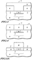
- FIG. 1 Shown in FIG. 1, in cross-section, is a portion of a semiconductor substrate 10 having already undergone several process steps in accordance with the invention.
- a gate oxide layer 12 overlies a principal surface 14 of semiconductor substrate 10, and a masking layer 16 overlies gate oxide layer 12.
- An opening 18 in masking layer 16 exposes a channel region 20 of semiconductor substrate 10.
- gate oxide layer 12 is formed by the thermal oxidation of principal surface 14 to form a silicon dioxide layer thereon.
- the thickness of gate oxide layer 12 can vary from about 40 to 150 angstroms depending upon the gate length of the MOS device being fabricated. For example, for the fabrication of an MOS transistor having a channel length of about 0.5 microns, the preferred gate oxide thickness is about 90 angstroms.
- Masking layer 16 is preferably silicon nitride deposited by chemical vapor deposition to a thickness of about 1500 to 3500 angstroms. To form opening 18, a photolithographic mask (not shown) is defined to overlie the deposited silicon nitride layer, and a reactive ion etching process is carried out to anisotropically etch the silicon nitride.
- the formation of symmetrically disposed doped regions in the channel region of an MOS transistor will now be described. It is important to note that the present invention contemplates the formation of both a single doped region in the channel region, and multiple doped regions within channel region 20.
- the illustrative embodiment described herein includes the formation of two doped regions. However, those skilled in the art will appreciate that the advantages of the invention can be obtained through the formation of only one of the doped regions described herein. Furthermore, it is also possible to form additional doped regions than those illustrated herein. For example, through the use of high energy ion implantation and the like.
- first doped region 22 is formed by the ion implantation of boron using an implant dose of about 5.0 E11 to 5.0 E12 ions/cm 2 at an implant energy of about 30 to 80 keV.
- the implant energy is adjusted depending upon the thickness of gate oxide layer 12 in order to place the peek concentration of the implanted boron atoms at a predetermined depth in semiconductor substrate 10.
- the peak dopant concentration of first doped region 22 about 1.0 E17 atoms/cm 3 and resides in substrate 10 at a distance of about 0.3 microns below principal surface 14.
- first doped region 22 can be formed by implantation of indium at a dose of about 8.0 E12 using an implant energy of about 120 keV.
- a second doped region 24 is formed in substrate 10 using one of two methods illustrated in FIG. 2A and FIG. 2B.
- a first semiconductor layer 26 is deposited by chemical vapor deposition to overlie masking layer 16 and the surface portion of substrate 10 exposed by opening 18.
- the first semiconductor layer 26 is polysilicon deposited to a thickness of about 1000 to 2000 angstroms, and most preferably about 1500 angstroms.
- the polysilicon is doped with phosphorus to increase the electrical conductivity.
- the doping process can be performed either during deposition or immediately afterward.
- other semiconductor materials can be deposited, such as refractory metal silicides and the like.
- the chemical vapor deposition process is adjusted to conformally deposit first polysilicon layer 26 to follow the contour of masking layer 16. As illustrated in FIG. 2A, the conformal deposition results in the formation of a depressed region in first semiconductor layer 26 located at the mid-point of the lateral dimension of opening 18. Accordingly, the vertical thickness of first semiconductor layer 26 equals the deposition thickness in the center of opening 18. By conformally depositing first semiconductor layer 26, a thickness differential is obtained in opening 18, which provides a precisely contoured implantation mask for the formation of second doped region 24.
- the ion implant parameters are adjusted, such that following an annealing cycle, second doped region 24 will extend from principal surface 14 into substrate 10 and contact first doped region 22.
- the ion implant energy employed will depend upon the deposited thickness of first semiconductor layer 26. For example, where the thickness of first semiconductor layer 26 is 1,000 angstroms, boron ions are implanted at an energy of about 20 to 60 keV, whereas if the deposited thickness of first semiconductor layer 26 is 3,000 angstroms, boron is implanted at an energy of about 80 to 120 keV.
- the ion implant process is adjusted to deliver a boron dose of about 5.0 E11 to 5.0 E13 ions/cm 2 .
- the particular boron dose and energy used will provide a peak concentration of boron at a depth of about 0.1 microns below principal surface 14, and a peak doping concentration of about 1.0 E17 to 5.0 E17 atoms/cm 3 .
- the doping processes of the invention provide a distribution of dopant atoms in the substrate. Although implant parameters are adjusted to place a peak doping concentration to a specified depth in the substrate, a certain amount of ranging and straggle is associated with the implant process. Although the figures illustrate ideal dopant distributions, some overlap of doping regions will occur.
- FIG. 2B An alternative method for the fabrication of second doped region 24 is illustrated in FIG. 2B.
- first semiconductor layer 26 is deposited according to the method described above.
- a reactive ion etching process is carried out to form sidewall spacers 28 adjacent to the walls of opening 18.
- the lateral extent of sidewall spacers 28 along principal surface 14 is determined by a number of process parameters.
- the process parameters include, the deposition thickness of the polysilicon layer, the thickness of masking layer 16, the etching time, and the like. Accordingly, the separation distance of sidewall spacers 28 is also determined by the aforementioned process parameters.
- the deposition thickness of the polysilicon layer is also determinative of the lateral extent of second doped region 24.
- the polysilicon layer is deposited to a thickness of about 1000 to 2000 angstroms and the etching time is adjusted to achieve the desired later distance in view of the deposition thickness of masking layer 16.
- the polysilicon deposition step illustrated in FIGs. 2A and 2B represents the first step in the fabrication of a gate electrode for the MOS device under construction.
- a second semiconductor layer 30 is deposited to overlie either first semiconductor layer 26, or sidewall spacers 28, depending upon the particular process employed to form second doped region 24.
- second semiconductor layer 30 is polysilicon deposited to a thickness of about 1000 to 2000 angstroms.
- second semiconductor layer 30 fills opening 18 and forms a somewhat planar surface overlying masking layer 16.
- second semiconductor layer 30 is carried out in such a manner as to form a somewhat planar surface, regardless of whether or not sidewall spacers are formed after depositing first semiconductor layer 26. Also, the formation of a planar surface is not essential to the process of the invention.
- a planarization process is carried out to form a planar surface 32, as illustrated in FIG. 4.
- a chemical-mechanical-polishing process is carried out to remove surface portions of second semiconductor layer 30, and if present, portions of first semiconductor layer 26. Additionally, a portion of the upper surface of masking layer 16 can also be removed during the polishing process.
- the polishing process employs an abrasive slurry composed of silica particles and a chemical etchant to grind away successive surface layers and form a smooth surface.
- the chemical composition of the slurry can be adjusted to selectively remove one material composition to that of another material compensation. Alternatively, the slurry can be adjusted to non-selectively remove many different kinds of material.
- a non-selective slurry is employed which removes polysilicon and silicon nitride at substantially the same rate. Accordingly, the polishing time will determine the vertical dimension of the polysilicon material overlying semiconductor substrate 10 in opening 18.
- planarization processes can be used to form planar surface 32.
- ion sputtering, focus molecular beam bombardment, non-selective plasma etching, and the like can be used to form planar surface 32.
- the planarization process is carried out for an amount of time sufficient to remove surface layers of polysilicon material, and to leave about 1000 to 3000 angstroms of polysilicon in opening 18 overlying principal surface 14.
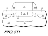
- FIG. 5A and FIG. 5B one of two different source drain configurations can be formed, as illustrated in FIG. 5A and FIG. 5B.
- masking layer 16 is removed leaving a gate electrode 34 overlying channel region 20 of semiconductor substrate 10. Gate electrode 34 is separated from channel region 20 by gate oxide layer 12.
- an ion implant process is carried out to form source and drain regions 36 and 38, respectively.
- source and drain regions 36 and 38 are formed by the ion implantation of either arsenic or phosphorous into semiconductor substrate 10 using gate electrode 34 as an implant mask.
- source and drain regions 36 and 38 are self-aligned to gate electrode 34 and are spaced apart in semiconductor substrate 10 by channel region 20.
- arsenic is used to form the source and drain regions
- the arsenic is preferably implanted using a dose of about 1.0 E15 to 5.0 E15 ions/cm 2 at an energy of about 30 to 80 keV.
- phosphorous is used, the phosphorous is preferably implanted using a dose of about 1.0 E15 to 5.0 E15 ions/cm 2 at an energy of about 20 to 60 keV.
- a lightly doped drain structure can be formed as illustrated in FIG. 5B.
- gate electrode 34 is defined by removing masking layer 16
- an ion implant process is carried out to form lightly doped regions 40 and 42, using gate electrode 34 as an implantation mask.
- a dielectric material is deposited to overlie substrate 10 and a reactive ion etching process is carried out to form dielectric sidewall spacers 44.
- the ion implant process described in relation to FIG. 5A is carried out to form source and drain regions 36 and 38, respectively.
- Lightly doped regions 40 and 42 are formed by the implantation of either arsenic or phosphorous.
- the phosphorous is preferably implanted using a dose of about 5.0 E12 to 1.0 E14 ions/cm 2 , at an implant energy of about 20 to 60 keV.
- the arsenic is preferably implanted using a dose of about 5.0 E12 to 1.0 E14 ion/cm 2 at an implant energy of about 30 to 80 keV.
- the ion implantation process to form source and drain regions 36 and 38 is performed such that following an annealing process, the source and drain regions will have a peak doping concentration of about 1.0 E21 atoms/cm 3 .
- the peak doping concentration of the source drain regions resides in substrate 10 about 0.1 microns below principal surface 14.
- the foregoing process description provides an n-channel MOS transistor preferably having a threshold voltage of about 0.2 to 0.4 volts, and most preferably about 0.35 volts.
- the device preferably exhibits an on-current of about 50 to 65 microamps/micron at a drain voltage of about 1.2 volts and a gate voltage of about 0.9 volts.
- a device fabricated in accordance with the invention preferably exhibits an off current of about 1 to 5 picoamps/micron at a drain voltage of about 1.2 volts and a gate voltage of about 0 volts.
- a device fabricated in accordance with the invention exhibits a body effect acting on the threshold voltage of about 100 to 200 millivolts at a substrate bias ranging from -2 volts to 0 volts.
- the foregoing parameters are the preferred operational characteristics of a device fabricated in accordance with the invention and operating at a supply voltage of preferably less than 5 volts.
- the process of the invention advantageously provides an MOS device that can operate a voltages substantially below 5 volts. For example, the device will perform at high efficiency at operating voltages of 3 volts to as low as about 1 volt.
- the gate electrode and channel region of the MOS device are defined by a patterned masking layer formed on the surface of semiconductor substrate 10. This process stands in distinct contrast to fabrication processes of the prior art.
- a patterned masking layer to define both the channel region and the gate electrode of an MOS device, a high degree of precision can be used in the fabrication of doped regions within the channel region of the device.
- the gate electrode is positioned directly over the channel region and self aligned to the channel region. The device is further refined by coupling the channel fabrication process with a self-aligned source-drain process to yield a submicron MOS transistor having superior performance characteristics.
- a fully functional MOS device exhibiting all of the advantages of the invention can be realized by omitting the fabrication of either first doped region 22 or second doped region 24. Additionally, for the fabrication of p-channel devices, phosphorus or antimony can be implanted into the channel region. It is therefore intended to include within the invention all such variations and modifications as fall within the scope of the appended claims and equivalents thereof.
Landscapes
- Insulated Gate Type Field-Effect Transistor (AREA)
Applications Claiming Priority (2)
| Application Number | Priority Date | Filing Date | Title |
|---|---|---|---|
| US395339 | 1995-02-28 | ||
| US08/395,339 US5605855A (en) | 1995-02-28 | 1995-02-28 | Process for fabricating a graded-channel MOS device |
Publications (2)
| Publication Number | Publication Date |
|---|---|
| EP0730293A2 true EP0730293A2 (de) | 1996-09-04 |
| EP0730293A3 EP0730293A3 (de) | 1997-11-05 |
Family
ID=23562631
Family Applications (1)
| Application Number | Title | Priority Date | Filing Date |
|---|---|---|---|
| EP96102457A Withdrawn EP0730293A3 (de) | 1995-02-28 | 1996-02-19 | Verfahren zur Herstellung einer MOS-Anordnung mit gradiertem Kanal |
Country Status (3)
| Country | Link |
|---|---|
| US (1) | US5605855A (de) |
| EP (1) | EP0730293A3 (de) |
| JP (1) | JPH08250715A (de) |
Cited By (9)
| Publication number | Priority date | Publication date | Assignee | Title |
|---|---|---|---|---|
| EP1054450A3 (de) * | 1999-05-18 | 2001-02-07 | Hiroshima University | MOSFET Halbleiterbauelement mit hochdotiertem Sperrgebiet |
| EP1024537A3 (de) * | 1998-12-28 | 2003-06-25 | Infineon Technologies North America Corp. | Feldeffekttransistor mit isoliertem Gate, der einen vergrabenen Bereich aufweist, und Verfahren zu dessen Herstellung |
| EP1071125A3 (de) * | 1999-07-22 | 2005-06-01 | International Business Machines Corporation | Verfahren zur Herstellung von Transistoren mit unabhängig einstellbaren Parametern |
| WO2012050783A1 (en) * | 2010-09-29 | 2012-04-19 | Analog Devices, Inc. | Field effect transistors having improved breakdown voltages and methods of forming the same |
| US8803193B2 (en) | 2011-05-11 | 2014-08-12 | Analog Devices, Inc. | Overvoltage and/or electrostatic discharge protection device |
| US8816389B2 (en) | 2011-10-21 | 2014-08-26 | Analog Devices, Inc. | Overvoltage and/or electrostatic discharge protection device |
| US10043792B2 (en) | 2009-11-04 | 2018-08-07 | Analog Devices, Inc. | Electrostatic protection device |
| US10181719B2 (en) | 2015-03-16 | 2019-01-15 | Analog Devices Global | Overvoltage blocking protection device |
| US10199482B2 (en) | 2010-11-29 | 2019-02-05 | Analog Devices, Inc. | Apparatus for electrostatic discharge protection |
Families Citing this family (29)
| Publication number | Priority date | Publication date | Assignee | Title |
|---|---|---|---|---|
| WO1996016432A2 (en) * | 1994-11-16 | 1996-05-30 | Matsushita Electric Industrial Co., Ltd. | Channel or source/drain structure of mosfet and method for fabricating the same |
| US6127700A (en) * | 1995-09-12 | 2000-10-03 | National Semiconductor Corporation | Field-effect transistor having local threshold-adjust doping |
| KR0167271B1 (ko) * | 1995-11-30 | 1998-12-15 | 문정환 | 비균등 도우프 채널 구조를 갖는 반도체소자의 제조방법 |
| KR0186071B1 (ko) * | 1995-12-29 | 1999-04-15 | 문정환 | 모스전계효과트랜지스터 제조방법 |
| KR0167301B1 (ko) * | 1995-12-29 | 1999-02-01 | 문정환 | 모스전계효과트랜지스터 제조방법 |
| US7195960B2 (en) * | 1996-06-28 | 2007-03-27 | Seiko Epson Corporation | Thin film transistor, manufacturing method thereof, and circuit and liquid crystal display device using the thin film transistor |
| TW326110B (en) * | 1996-12-24 | 1998-02-01 | Nat Science Council | Manufacturing method for inversed T-type well component |
| US6093951A (en) * | 1997-06-30 | 2000-07-25 | Sun Microsystems, Inc. | MOS devices with retrograde pocket regions |
| US6025232A (en) | 1997-11-12 | 2000-02-15 | Micron Technology, Inc. | Methods of forming field effect transistors and related field effect transistor constructions |
| US5877056A (en) * | 1998-01-08 | 1999-03-02 | Texas Instruments-Acer Incorporated | Ultra-short channel recessed gate MOSFET with a buried contact |
| US6117742A (en) * | 1998-05-15 | 2000-09-12 | Advanced Micro Devices, Inc. | Method for making a high performance transistor |
| US6249027B1 (en) | 1998-06-08 | 2001-06-19 | Sun Microsystems, Inc. | Partially depleted SOI device having a dedicated single body bias means |
| JP2000049344A (ja) * | 1998-07-31 | 2000-02-18 | Mitsubishi Electric Corp | 半導体装置およびその製造方法 |
| US6117739A (en) * | 1998-10-02 | 2000-09-12 | Advanced Micro Devices, Inc. | Semiconductor device with layered doped regions and methods of manufacture |
| US6395606B1 (en) * | 1999-07-21 | 2002-05-28 | Advanced Micro Devices, Inc. | MOSFET with metal in gate for reduced gate resistance |
| US6797576B1 (en) | 2000-03-31 | 2004-09-28 | National Semiconductor Corporation | Fabrication of p-channel field-effect transistor for reducing junction capacitance |
| US6548842B1 (en) | 2000-03-31 | 2003-04-15 | National Semiconductor Corporation | Field-effect transistor for alleviating short-channel effects |
| US6566204B1 (en) | 2000-03-31 | 2003-05-20 | National Semiconductor Corporation | Use of mask shadowing and angled implantation in fabricating asymmetrical field-effect transistors |
| US7145191B1 (en) | 2000-03-31 | 2006-12-05 | National Semiconductor Corporation | P-channel field-effect transistor with reduced junction capacitance |
| US6531410B2 (en) | 2001-02-27 | 2003-03-11 | International Business Machines Corporation | Intrinsic dual gate oxide MOSFET using a damascene gate process |
| US6821855B2 (en) * | 2002-08-29 | 2004-11-23 | Micron Technology, Inc. | Reverse metal process for creating a metal silicide transistor gate structure |
| KR100620064B1 (ko) * | 2004-12-28 | 2006-09-08 | 주식회사 하이닉스반도체 | 반도체장치의 스토리지노드콘택 형성 방법 |
| US7354831B2 (en) * | 2005-08-08 | 2008-04-08 | Freescale Semiconductor, Inc. | Multi-channel transistor structure and method of making thereof |
| JP2007214495A (ja) * | 2006-02-13 | 2007-08-23 | Oki Electric Ind Co Ltd | 半導体装置および半導体装置の製造方法 |
| US8004038B2 (en) * | 2006-05-22 | 2011-08-23 | Taiwan Semiconductor Manufacturing Company, Ltd. | Suppression of hot-carrier effects using double well for thin gate oxide LDMOS embedded in HV process |
| US8664067B2 (en) * | 2010-11-18 | 2014-03-04 | Monolithic Power Systems, Inc. | CMOS devices with reduced short channel effects |
| JP5997426B2 (ja) * | 2011-08-19 | 2016-09-28 | 株式会社日立製作所 | 半導体装置および半導体装置の製造方法 |
| CN103915483B (zh) * | 2012-12-28 | 2019-06-14 | 瑞萨电子株式会社 | 具有被改造以减少漏电流的沟道芯部的场效应晶体管及制作方法 |
| CN114335161A (zh) * | 2021-12-29 | 2022-04-12 | 深圳市千屹芯科技有限公司 | 一种具有渐变掺杂沟道的SiC MOSFET器件及其制备工艺 |
Family Cites Families (24)
| Publication number | Priority date | Publication date | Assignee | Title |
|---|---|---|---|---|
| JPS53112069A (en) * | 1977-03-11 | 1978-09-30 | Nippon Telegr & Teleph Corp <Ntt> | Production of mis transistor |
| JPS55113359A (en) * | 1979-02-22 | 1980-09-01 | Fujitsu Ltd | Semiconductor integrated circuit device |
| US4599118A (en) * | 1981-12-30 | 1986-07-08 | Mostek Corporation | Method of making MOSFET by multiple implantations followed by a diffusion step |
| JPS60196974A (ja) * | 1984-03-19 | 1985-10-05 | Toshiba Corp | 導電変調型mosfet |
| US4697198A (en) * | 1984-08-22 | 1987-09-29 | Hitachi, Ltd. | MOSFET which reduces the short-channel effect |
| JPS6252969A (ja) * | 1985-08-30 | 1987-03-07 | Nippon Texas Instr Kk | 絶縁ゲ−ト型電界効果半導体装置 |
| US5082794A (en) * | 1989-02-13 | 1992-01-21 | Motorola, Inc. | Method of fabricating mos transistors using selective polysilicon deposition |
| US5073512A (en) * | 1989-04-21 | 1991-12-17 | Nec Corporation | Method of manufacturing insulated gate field effect transistor having a high impurity density region beneath the channel region |
| JP2548994B2 (ja) * | 1990-03-19 | 1996-10-30 | 富士通株式会社 | 電界効果型トランジスタ及びその製造方法 |
| KR940006702B1 (ko) * | 1991-06-14 | 1994-07-25 | 금성일렉트론 주식회사 | 모스패트의 제조방법 |
| US5266508A (en) * | 1991-08-26 | 1993-11-30 | Sharp Kabushiki Kaisha | Process for manufacturing semiconductor device |
| JPH06132524A (ja) * | 1992-10-16 | 1994-05-13 | Sanyo Electric Co Ltd | 半導体装置の製造方法 |
| US5399508A (en) * | 1993-06-23 | 1995-03-21 | Vlsi Technology, Inc. | Method for self-aligned punchthrough implant using an etch-back gate |
| US5374574A (en) * | 1993-11-23 | 1994-12-20 | Goldstar Electron Co., Ltd. | Method for the fabrication of transistor |
| US5374575A (en) * | 1993-11-23 | 1994-12-20 | Goldstar Electron Co., Ltd. | Method for fabricating MOS transistor |
| US5372960A (en) * | 1994-01-04 | 1994-12-13 | Motorola, Inc. | Method of fabricating an insulated gate semiconductor device |
| US5482878A (en) * | 1994-04-04 | 1996-01-09 | Motorola, Inc. | Method for fabricating insulated gate field effect transistor having subthreshold swing |
| US5427964A (en) * | 1994-04-04 | 1995-06-27 | Motorola, Inc. | Insulated gate field effect transistor and method for fabricating |
| US5434093A (en) * | 1994-08-10 | 1995-07-18 | Intel Corporation | Inverted spacer transistor |
| US5429956A (en) * | 1994-09-30 | 1995-07-04 | United Microelectronics Corporation | Method for fabricating a field effect transistor with a self-aligned anti-punchthrough implant channel |
| US5489543A (en) * | 1994-12-01 | 1996-02-06 | United Microelectronics Corp. | Method of forming a MOS device having a localized anti-punchthrough region |
| US5472897A (en) * | 1995-01-10 | 1995-12-05 | United Microelectronics Corp. | Method for fabricating MOS device with reduced anti-punchthrough region |
| US5484743A (en) * | 1995-02-27 | 1996-01-16 | United Microelectronics Corporation | Self-aligned anti-punchthrough implantation process |
| US5538913A (en) * | 1995-11-13 | 1996-07-23 | United Microelectronics Corporation | Process for fabricating MOS transistors having full-overlap lightly-doped drain structure |
-
1995
- 1995-02-28 US US08/395,339 patent/US5605855A/en not_active Expired - Fee Related
-
1996
- 1996-02-16 JP JP8054037A patent/JPH08250715A/ja active Pending
- 1996-02-19 EP EP96102457A patent/EP0730293A3/de not_active Withdrawn
Cited By (10)
| Publication number | Priority date | Publication date | Assignee | Title |
|---|---|---|---|---|
| EP1024537A3 (de) * | 1998-12-28 | 2003-06-25 | Infineon Technologies North America Corp. | Feldeffekttransistor mit isoliertem Gate, der einen vergrabenen Bereich aufweist, und Verfahren zu dessen Herstellung |
| EP1054450A3 (de) * | 1999-05-18 | 2001-02-07 | Hiroshima University | MOSFET Halbleiterbauelement mit hochdotiertem Sperrgebiet |
| EP1071125A3 (de) * | 1999-07-22 | 2005-06-01 | International Business Machines Corporation | Verfahren zur Herstellung von Transistoren mit unabhängig einstellbaren Parametern |
| US10043792B2 (en) | 2009-11-04 | 2018-08-07 | Analog Devices, Inc. | Electrostatic protection device |
| WO2012050783A1 (en) * | 2010-09-29 | 2012-04-19 | Analog Devices, Inc. | Field effect transistors having improved breakdown voltages and methods of forming the same |
| US8476684B2 (en) | 2010-09-29 | 2013-07-02 | Analog Devices, Inc. | Field effect transistors having improved breakdown voltages and methods of forming the same |
| US10199482B2 (en) | 2010-11-29 | 2019-02-05 | Analog Devices, Inc. | Apparatus for electrostatic discharge protection |
| US8803193B2 (en) | 2011-05-11 | 2014-08-12 | Analog Devices, Inc. | Overvoltage and/or electrostatic discharge protection device |
| US8816389B2 (en) | 2011-10-21 | 2014-08-26 | Analog Devices, Inc. | Overvoltage and/or electrostatic discharge protection device |
| US10181719B2 (en) | 2015-03-16 | 2019-01-15 | Analog Devices Global | Overvoltage blocking protection device |
Also Published As
| Publication number | Publication date |
|---|---|
| JPH08250715A (ja) | 1996-09-27 |
| US5605855A (en) | 1997-02-25 |
| EP0730293A3 (de) | 1997-11-05 |
Similar Documents
| Publication | Publication Date | Title |
|---|---|---|
| US5605855A (en) | Process for fabricating a graded-channel MOS device | |
| US5668021A (en) | Process for fabricating a semiconductor device having a segmented channel region | |
| EP0507567B1 (de) | Feldeffekttransistorstruktur und Verfahren zur Herstellung | |
| US6518138B2 (en) | Method of forming Self-aligned lateral DMOS with spacer drift region | |
| US5489543A (en) | Method of forming a MOS device having a localized anti-punchthrough region | |
| US6300205B1 (en) | Method of making a semiconductor device with self-aligned active, lightly-doped drain, and halo regions | |
| US7297606B2 (en) | Metal-oxide-semiconductor device including a buried lightly-doped drain region | |
| US6201278B1 (en) | Trench transistor with insulative spacers | |
| US5962894A (en) | Trench transistor with metal spacers | |
| US5102816A (en) | Staircase sidewall spacer for improved source/drain architecture | |
| US6501139B1 (en) | High-voltage transistor and fabrication process | |
| US5627097A (en) | Method for making CMOS device having reduced parasitic capacitance | |
| US5937301A (en) | Method of making a semiconductor device having sidewall spacers with improved profiles | |
| US6200863B1 (en) | Process for fabricating a semiconductor device having assymetric source-drain extension regions | |
| US6114211A (en) | Semiconductor device with vertical halo region and methods of manufacture | |
| US6365475B1 (en) | Method of forming a MOS transistor | |
| US6274443B1 (en) | Simplified graded LDD transistor using controlled polysilicon gate profile | |
| US5646435A (en) | Method for fabricating CMOS field effect transistors having sub-quarter micrometer channel lengths with improved short channel effect characteristics | |
| US6767778B2 (en) | Low dose super deep source/drain implant | |
| US6261885B1 (en) | Method for forming integrated circuit gate conductors from dual layers of polysilicon | |
| US7419867B2 (en) | CMOS gate structure comprising predoped semiconductor gate material with improved uniformity of dopant distribution and method of forming the structure | |
| US6287922B1 (en) | Method for fabricating graded LDD transistor using controlled polysilicon gate profile | |
| US5547882A (en) | Method for forming retrograde channel profile by phosphorus implantation through polysilicon gate | |
| US5976925A (en) | Process of fabricating a semiconductor devise having asymmetrically-doped active region and gate electrode | |
| US6323561B1 (en) | Spacer formation for precise salicide formation |
Legal Events
| Date | Code | Title | Description |
|---|---|---|---|
| PUAI | Public reference made under article 153(3) epc to a published international application that has entered the european phase |
Free format text: ORIGINAL CODE: 0009012 |
|
| AK | Designated contracting states |
Kind code of ref document: A2 Designated state(s): DE FR GB IT |
|
| PUAL | Search report despatched |
Free format text: ORIGINAL CODE: 0009013 |
|
| AK | Designated contracting states |
Kind code of ref document: A3 Designated state(s): DE FR GB IT |
|
| 17P | Request for examination filed |
Effective date: 19971223 |
|
| STAA | Information on the status of an ep patent application or granted ep patent |
Free format text: STATUS: THE APPLICATION HAS BEEN WITHDRAWN |
|
| 18W | Application withdrawn |
Withdrawal date: 19981130 |