EP0727932A2 - Electromagnetic shielded casing - Google Patents
Electromagnetic shielded casing Download PDFInfo
- Publication number
- EP0727932A2 EP0727932A2 EP95308494A EP95308494A EP0727932A2 EP 0727932 A2 EP0727932 A2 EP 0727932A2 EP 95308494 A EP95308494 A EP 95308494A EP 95308494 A EP95308494 A EP 95308494A EP 0727932 A2 EP0727932 A2 EP 0727932A2
- Authority
- EP
- European Patent Office
- Prior art keywords
- housing
- shield member
- locating means
- ground pattern
- conductive layer
- Prior art date
- Legal status (The legal status is an assumption and is not a legal conclusion. Google has not performed a legal analysis and makes no representation as to the accuracy of the status listed.)
- Granted
Links
Images


Classifications
-
- H—ELECTRICITY
- H05—ELECTRIC TECHNIQUES NOT OTHERWISE PROVIDED FOR
- H05K—PRINTED CIRCUITS; CASINGS OR CONSTRUCTIONAL DETAILS OF ELECTRIC APPARATUS; MANUFACTURE OF ASSEMBLAGES OF ELECTRICAL COMPONENTS
- H05K9/00—Screening of apparatus or components against electric or magnetic fields
- H05K9/0007—Casings
- H05K9/002—Casings with localised screening
- H05K9/0039—Galvanic coupling of ground layer on printed circuit board [PCB] to conductive casing
-
- H—ELECTRICITY
- H04—ELECTRIC COMMUNICATION TECHNIQUE
- H04B—TRANSMISSION
- H04B1/00—Details of transmission systems, not covered by a single one of groups H04B3/00 - H04B13/00; Details of transmission systems not characterised by the medium used for transmission
- H04B1/38—Transceivers, i.e. devices in which transmitter and receiver form a structural unit and in which at least one part is used for functions of transmitting and receiving
- H04B1/3827—Portable transceivers
- H04B1/3833—Hand-held transceivers
Definitions
- This invention is generally related to an electromagnetic shield structure for use in an electronic apparatus, and more particularly to a shield structure of reduced size and which lightens the electronic apparatus.
- a conventional radio communication apparatus includes a first housing 10, a second housing 20, and a printed circuit board 30 (called PC board hereinafter). Many components 31 are mounted on the PC board 30. A screw 40 is fitted to a threaded socket 12, thereby the PC board 30 and the first housing are fitted to the second housing 20.
- Figure 20 shows apparatus using a conventional shield structure.
- a partial view illustrated by one dot line A is shown in Figure 21 and it will be seen that conductive layer 21 is plated on an inner surface of the second housing 20.
- a first ground pattern 32 is printed on a surface of the PC board 30, while a second ground pattern 33 is printed on another surface of the PC board 30.
- the second housing 20 has a protruding portion 22.
- the protruding portion 22 is urged toward the first ground pattern 32 and thereby contacts the first ground pattern 32.
- This structure enables the components 31 to be shielded by the conductive layer 21, the first ground pattern 32 and the second ground pattern 33.
- a conductive contact member 23 may be provided between the protruding portion 22 and the first ground pattern 32 as shown in Figure 22.
- the second housing 20 includes a moulded resin member 26 and a conductive layer 21.
- the resin member 26 is formed by injection moulding and is then subjected to a conductive layer plating process. While the molded resin member 26 is being conveyed to the conductive layer plating process, it is necessary to treat the molded resin member 26 with great care so that it is not damaged.
- FIG 23 Another type of conventional structure is shown in Figure 23.
- a housing 20a is made of resin material.
- the components 31 are shielded by each of a plurality of conductive shield cases 34.
- a partial view illustrated by one dot lines B is shown in Figure 24.
- Each of the shield cases 34 is attached to the first ground pattern 32 on the PC board by soldering.
- the present invention has been made in view of the above circumstances and seeks to provide an electronic apparatus which eliminates the need for plating a conductive layer on a housing surface of the electronic apparatus.
- the present invention also seeks to provide an electronic apparatus having a housing which is suitable for recycling.
- the present invention also seeks to provide a configuration for an electronic apparatus which reduces the amount of dead space in the housing and thereby reduces the size and the weight of the apparatus.
- the present invention provides a shield member for use in an electronic apparatus including a housing, the housing having a first locating means, the shield member being attached to a circuit board having a ground pattern and being characterised by: a second locating means mating with the first locating means and a conductive layer, whereby, in use, the shield member is clamped between the circuit board and the housing, and the conductive layer contacts the ground pattern.
- the invention also extends to an electronic apparatus comprising, a circuit board having a ground pattern, components mounted on the circuit board, a housing including a first locating means and a shield member for shielding the components, having a second locating means mating with the first locating means and a conductive layer provided on the shield member, wherein the shield member is clamped between the circuit board and the housing, and the conductive layer contacts the ground pattern.
- Figure 1 shows a radio telecommunication apparatus (referred to hereinafter as an apparatus) including a shield structure of the present invention.
- the apparatus includes a first housing 110, a second housing 120 with a space 121, a PC board 130 and a shield case 140 mating with the space 121 for shielding components 131 mounted on the PC board 130.
- a ground pattern 132 is printed on the PC board 130.
- the first housing 110 is fitted to the second housing 120 by a male screw 122 and female screw 112 mating with the male screw 122.
- This structure is illustrated in Figure 2 in detail which is a cross-sectional view taken along line X-X.
- the second housing 120 has a protruding portion 124 as a first location determination portion.
- the shield case 140 includes a groove portion 144 mating with the protruding portion 12.
- the groove portion 144 serves as a second location determination portion. Since the groove portion mates with the protruding portion, the shield case 140 is located at a predetermined area of the second housing 120.
- the shield case 140 includes a resin member 146 and a conductive layer 142 plated on an inner surface of the resin member 146.
- the shield case 140 is clamped between the circuit board 130 and the second housing 120 by the male and female screws as shown in Figure 1, the shield case 140 is urged toward the PC board 130. Therefore, the conductive layer 142 contacts the first ground pattern 132.
- the groove portion 144 mates with the protruding portion 124.
- the shield case 140 is located at a predetermined area of the second housing 120.
- the conductive layer 142 on the groove portion 144 contacts the first ground pattern 132. Therefore, the groove portion 144 serves as a wall for isolating a component 131a and a component 131b, and for dividing the space enclosed by the shield case 140 and the PC board 130, into a plurality of space.
- the shield case 140 is made by the following process illustrated by Figures 5 and 6.
- a resin member is formed by resin injection moulding so that the deformed resin member 146 mates with the protruding portion 124 and the space 121 of the second housing 120.
- the conductive layer 142 is plated in the inner surface of the resin member 146, a flange portion 145 of the shield case 140 and the other surface 147 of the groove portion 144.
- the resin member 146 has 0.15mm - 0.25mm thickness and approximately 0.6g weight.
- the housing has 1mm - 2.5mm thickness and approximately 1.5g weight. Therefore, the resin member 146 is much thinner than the second housing 120 and much lighter than the second housing 120.
- the resin member 146 may be made of polyester resin, (“PET”), polycarbonate (“PC”), polyvinyl chloride (“PVC”) or ABS (acrylonitrile butadiene styrene). Relevant properties of each of these materials are compared in Figure 7. This shows that PC and ABS are most suitable for the resin member 146 having regard to heat suitability and age softening. PC is widely used and cheaper and therefore preferable to ABS
- the conductive layer 142 is plated on the inner surface of the resin member 146.
- the conductive layer 142 may be provided on the resin member 146 by other methods well known in the art, such as painting, sputtering, ion plating, evapolated metal attaching method which attaches evapolated metal to a resin object in vacuum air.
- the conductive layer 142 includes Ni(Nickel), Cu(Copper).
- the conductive layer 142 may include Au(Gold), Ag(silver). Further, the conductive layer 142 has 1 ⁇ m-3 ⁇ m thickness.
- a shield case 148 includes holes 149.
- a conductive layer 142C is also provided on an inner surface of the holes 149.
- the conductive layer 142B on the outer surface is connected with the conductive layer 142A on the inner surface via the conductive layer 142C on the holes 149.
- the holes have a wavelength/50 pitch, where the apparatus communicates signals with a base station over a radio channel having the wavelength. In this state, electromagnetic signals are not inserted into the shield case 148 via the holes 149, and the components in the shield case 148 does not radiate electromagnetic signals outside.
- the shielding efficiency of the shield case 148 of this structure is about the same as the conventional structure with the conductive shield case having the same thickness as that of the shield case 148.
- the shield case 140 mates with the space 121 of the second housing 120 and the protruding portion 124 and is clamped by the PC board 130 and the second housing 120 when the first housing 110 is fitted to the second housing 120 by the male and female threaded members 112 and 122. Therefore, deadspace between the second housing 120 and the shield case 140 is eliminated.
- the shield case 140 is separated from the housing 120. Therefore, it is easy to dispose of the second housing 120 without the conductive layer. Therefore, this structure is suitable for disposal and recycle of resin material.
- the shield case is urged toward the PC board by the screw connection and is very thin, and the flange portion 145 and the other surface 147 of the groove portion 144 are very flexible. Therefore, it is unnecessary to solder the shield case to the PC board like the conventional structure. Further, the shield case 140 is firmly connected with the first ground pattern 132 by the resilience of the flange portion 145 and the other surface 147 of the groove portion 144.
- the flange portion 145 and the other surface 147 of the groove portion 144 may have other structures as shown in Figure 10.
- the flange portion 145 and the other surface 147 of the groove portion 144 have tongues 152 and grooves 154.
- the tongue 152 When the first housing is fitted to the second housing, the tongue 152, as shown in Figure 11a, is urged towards the PC board 130, and thereby is deformed as shown in Figure 11b.
- This structure enhances the connection between the shield case 140a and the ground pattern 132 on the PC board 130.
- the shape of the tongue 152 becomes the initiate shape as shown in Figure 11a by elasticity of the tongue 152.
- a shield case 140b has a plurality of hemispheres 156 on the flange portion 145 and the other surface 147 of the groove portion 144.
- Each of the hemispheres 156 is arranged with a predetermined separation distance and has elasticity.
- a shield case 140°C has a first conductive layer 140 for shielding the components and a second conductive layer 158 for connecting a first signal pattern 136 with a second signal pattern 138.
- the second conductive layer 158 is connected with a first land 136a coupled to the first signal pattern 136 and a second land 138a coupled to the second signal pattern 138.
- the shield case 140c shields the components 131 and also connects the first signal pattern 136 and the second signal patter 138.
- an elastic member 160 such as a foamed material may be arranged between the protruding portion 124 of the second housing 120 and the groove portion 144 of the shield case 140.
- the resin is formed by an injection moulding method so that the resin member 146 mates with the second housing.
- the conductive layer 142 is provided on the resin member 146.
- a metal plate may be formed as shown in Figure 17.
- a metal plate 162 as shown in Figure 17a such as copper plated with nickel is deformed by a well known method such as plastic deformation so that the formed metal plate 162 mates with the second housing as shown in Figure 17b.
- the metal plate 162 is 0.1mm thickness.
- the resin plate plated with a conductive layer such as nickel and copper may be deformed by the plastic deformation.
- a plurality of slits 166 may be provided at the plate as shown in Figure 18.
- a metal plate 164 has a plurality of slits 166 as shown in Figure 18a. After the plastic deformation of the plate 164, the slits 166 becomes holes 168 Figure 18b. Therefore, the structure facilitates the plastic deformation.
- each hole 168 has a pitch of ⁇ 50, where the apparatus communicates with a base station over a radio channel having the wavelength ⁇ . Therefore, electromagnetic signals cannot penetrate the shield case via the holes, and the components in the shield case do not radiate electromagnetic signals outside.
- protruding portion 124 serves as a first locating means and the grooved portion 144 serves as a second location means, their positions may of course be interchanged.
- the flange portion 145 and the other surface 147 of the groove portion 144 are provided with tongues 152 and hemispheres 156, the flange portion 145 and the other surface 147 of the groove portion 144 may be deformed in advance so that they have portions curved toward the PC board which provide resilience.
Abstract
Description
- This invention is generally related to an electromagnetic shield structure for use in an electronic apparatus, and more particularly to a shield structure of reduced size and which lightens the electronic apparatus.
- Referring to Figure 19, a conventional radio communication apparatus includes a
first housing 10, asecond housing 20, and a printed circuit board 30 (called PC board hereinafter).Many components 31 are mounted on thePC board 30. A screw 40 is fitted to a threadedsocket 12, thereby thePC board 30 and the first housing are fitted to thesecond housing 20. - To electrically shield the
components 31, various shield structures are used in conventional apparatus. Figure 20 shows apparatus using a conventional shield structure. A partial view illustrated by one dot line A is shown in Figure 21 and it will be seen thatconductive layer 21 is plated on an inner surface of thesecond housing 20. - A
first ground pattern 32 is printed on a surface of thePC board 30, while asecond ground pattern 33 is printed on another surface of thePC board 30. Thesecond housing 20 has a protrudingportion 22. - When the
first housing 10 and thePC board 30 are fitted to thesecond housing 20, the protrudingportion 22 is urged toward thefirst ground pattern 32 and thereby contacts thefirst ground pattern 32. This structure enables thecomponents 31 to be shielded by theconductive layer 21, thefirst ground pattern 32 and thesecond ground pattern 33. - Further, to enhance the connection between the
conductive layer 21 and thefirst ground pattern 32, aconductive contact member 23 may be provided between the protrudingportion 22 and thefirst ground pattern 32 as shown in Figure 22. - In the above conventional forms of apparatus, the
second housing 20 includes amoulded resin member 26 and aconductive layer 21. Theresin member 26 is formed by injection moulding and is then subjected to a conductive layer plating process. While the moldedresin member 26 is being conveyed to the conductive layer plating process, it is necessary to treat the moldedresin member 26 with great care so that it is not damaged. - Further, in the plating process, it is necessary to mask a predetermined area of the inner surface of the
member 26 so that theconductive layer 21 is plated only onto regions other than the masked area. This involves another costly manufacturing step. - Furthermore, when the radio telecommunication apparatus comes to the end of its useful life, it is not easy to separate the
conductive layer 21 from theresin member 26, and thus the materials are difficult to recycle. - Another type of conventional structure is shown in Figure 23. A housing 20a is made of resin material. The
components 31 are shielded by each of a plurality ofconductive shield cases 34. A partial view illustrated by one dot lines B is shown in Figure 24. Each of theshield cases 34 is attached to thefirst ground pattern 32 on the PC board by soldering. - In this structure, an extra process is required to solder the
shield case 34 to thePC board 30. Further, since extra space is needed between theshield case 34 and the housing 20a the apparatus becomes larger and heavier. - Accordingly, the present invention has been made in view of the above circumstances and seeks to provide an electronic apparatus which eliminates the need for plating a conductive layer on a housing surface of the electronic apparatus.
- The present invention also seeks to provide an electronic apparatus having a housing which is suitable for recycling.
- The present invention also seeks to provide a configuration for an electronic apparatus which reduces the amount of dead space in the housing and thereby reduces the size and the weight of the apparatus.
- Accordingly the present invention provides a shield member for use in an electronic apparatus including a housing, the housing having a first locating means, the shield member being attached to a circuit board having a ground pattern and being characterised by:
a second locating means mating with the first locating means and a conductive layer, whereby, in use,
the shield member is clamped between the circuit board and the housing, and the conductive layer contacts the ground pattern. - The invention also extends to an electronic apparatus comprising, a circuit board having a ground pattern, components mounted on the circuit board, a housing including a first locating means and a shield member for shielding the components, having a second locating means mating with the first locating means and a conductive layer provided on the shield member, wherein the shield member is clamped between the circuit board and the housing, and the conductive layer contacts the ground pattern.
- Some embodiments of the invention will now be described by way of example only with reference to the accompanying drawings in which:
- Figure 1 is a perspective view illustrating a radio telecommunication apparatus according to a first embodiment of the present invention;
- Figure 2 is a cross-sectional view taken along line X-X of Figure 1;
- Figure 3 is a partial cross-sectional view illustrating a portion C of Figure 2;
- Figure 4 is a partial cross-sectional view illustrating a portion D of Figure 2;
- Figure 5 is a first step of a manufacturing process for a shield member;
- Figure 6 is a second step of the manufacturing process;
- Figure 7 is a table comprising properties of some materials;
- Figure 8 is a perspective view illustrating a shield member according to a second embodiment;
- Figure 9 is a partial cross-sectional view of the embodiment illustrated in Figure 8;
- Figure 10 is a perspective view illustrating a shield member according to a third embodiment;
- Figure 11 is a partial cross-sectional view illustrating the attachment state of the shield member according to the third embodiment;
- Figure 12 is a perspective view illustrating a shield member according to a fourth embodiment;
- Figure 13 is a partial cross-sectional view illustrating the mounting of the shield member according to the fourth embodiment;
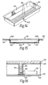
- Figure 14 is a perspective view illustrating a shield member according to a fifth embodiment;
- Figure 15 is a partial cross-sectional view illustrating the mounting of the shield member according to the fifth embodiment;
- Figure 16 is a partial cross-sectional view illustrating a shield member according to a sixth embodiment;
- Figure 17 is a perspective view illustrating a manufacturing process in which a shield member according to a seventh embodiment is manufactured;
- Figure 18 is a perspective view illustrating a manufacturing process in which a shield member according to an eighth embodiment is manufactured;
- Figure 19 is a perspective view illustrating a first conventional radio telecommunication apparatus;
- Figure 20 is a cross-sectional view taken along line Y-Y of Figure 19;
- Figure 21 is a partial cross-sectional view illustrating a portion A of Figure 20;
- Figure 22 is a partial cross-sectional view illustrating a second conventional apparatus;
- Figure 23 is a cross-sectional view illustrating a third conventional apparatus including a third conventional structure; and
- Figure 24 is a partial cross-sectional view illustrating a portion B of Figure 23.
- Referring to the drawings,
Figure 1 shows a radio telecommunication apparatus (referred to hereinafter as an apparatus) including a shield structure of the present invention. - The apparatus includes a
first housing 110, asecond housing 120 with aspace 121, aPC board 130 and ashield case 140 mating with thespace 121 forshielding components 131 mounted on thePC board 130. Aground pattern 132 is printed on thePC board 130. Thefirst housing 110 is fitted to thesecond housing 120 by amale screw 122 andfemale screw 112 mating with themale screw 122. This structure is illustrated in Figure 2 in detail which is a cross-sectional view taken along line X-X. - Referring to Figure 2, the
second housing 120 has a protrudingportion 124 as a first location determination portion. Theshield case 140 includes agroove portion 144 mating with the protrudingportion 12. Thegroove portion 144 serves as a second location determination portion. Since the groove portion mates with the protruding portion, theshield case 140 is located at a predetermined area of thesecond housing 120. - A first partial structure illustrated by one dot line C is shown in Figure 3, while a second partial structure illustrated by one dot line D is shown in Figure 4. Referring to Figure 3, the
shield case 140 includes aresin member 146 and aconductive layer 142 plated on an inner surface of theresin member 146. When theshield case 140 is clamped between thecircuit board 130 and thesecond housing 120 by the male and female screws as shown in Figure 1, theshield case 140 is urged toward thePC board 130. Therefore, theconductive layer 142 contacts thefirst ground pattern 132. - Referring to Figure 4, the
groove portion 144 mates with the protrudingportion 124. Thereby theshield case 140 is located at a predetermined area of thesecond housing 120. Further, theconductive layer 142 on thegroove portion 144 contacts thefirst ground pattern 132. Therefore, thegroove portion 144 serves as a wall for isolating acomponent 131a and acomponent 131b, and for dividing the space enclosed by theshield case 140 and thePC board 130, into a plurality of space. - The
shield case 140 is made by the following process illustrated by Figures 5 and 6. In a first step illustrated by Figure 5, a resin member is formed by resin injection moulding so that thedeformed resin member 146 mates with the protrudingportion 124 and thespace 121 of thesecond housing 120. In a second step, theconductive layer 142 is plated in the inner surface of theresin member 146, aflange portion 145 of theshield case 140 and theother surface 147 of thegroove portion 144. - The
resin member 146 has 0.15mm - 0.25mm thickness and approximately 0.6g weight. The housing has 1mm - 2.5mm thickness and approximately 1.5g weight. Therefore, theresin member 146 is much thinner than thesecond housing 120 and much lighter than thesecond housing 120. - It will be appreciated that various forming processes may be used such as vacuum forming, plug assist forming, or injection moulding with vacuum which assists fluid resin flow in a mould.
- The
resin member 146 may be made of polyester resin, ("PET"), polycarbonate ("PC"), polyvinyl chloride ("PVC") or ABS (acrylonitrile butadiene styrene). Relevant properties of each of these materials are compared in Figure 7. This shows that PC and ABS are most suitable for theresin member 146 having regard to heat suitability and age softening. PC is widely used and cheaper and therefore preferable to ABS - The
conductive layer 142 is plated on the inner surface of theresin member 146. However, theconductive layer 142 may be provided on theresin member 146 by other methods well known in the art, such as painting, sputtering, ion plating, evapolated metal attaching method which attaches evapolated metal to a resin object in vacuum air. - The
conductive layer 142 includes Ni(Nickel), Cu(Copper). Theconductive layer 142 may include Au(Gold), Ag(silver). Further, theconductive layer 142 has 1µm-3µm thickness. - Although the
conductive layer 142 is provided on the inner surface of theresin member 146, the conductive layer may be provided on the outer surface of theresin member 146 as shown in Figures 8 and 9. Ashield case 148 includesholes 149. A conductive layer 142C is also provided on an inner surface of theholes 149. Thereby, theconductive layer 142B on the outer surface is connected with theconductive layer 142A on the inner surface via the conductive layer 142C on theholes 149. The holes have a wavelength/50 pitch, where the apparatus communicates signals with a base station over a radio channel having the wavelength. In this state, electromagnetic signals are not inserted into theshield case 148 via theholes 149, and the components in theshield case 148 does not radiate electromagnetic signals outside. - In this arrangement, the shielding efficiency of the
shield case 148 of this structure is about the same as the conventional structure with the conductive shield case having the same thickness as that of theshield case 148. - As mentioned above, the
shield case 140 mates with thespace 121 of thesecond housing 120 and the protrudingportion 124 and is clamped by thePC board 130 and thesecond housing 120 when thefirst housing 110 is fitted to thesecond housing 120 by the male and female threadedmembers second housing 120 and theshield case 140 is eliminated. - Further, it is unnecessary to place a conductive layer on the housing.
- Furthermore when the
screw 122 is removed from the threadedsocket 112, theshield case 140 is separated from thehousing 120. Therefore, it is easy to dispose of thesecond housing 120 without the conductive layer. Therefore, this structure is suitable for disposal and recycle of resin material. - The shield case is urged toward the PC board by the screw connection and is very thin, and the
flange portion 145 and theother surface 147 of thegroove portion 144 are very flexible. Therefore, it is unnecessary to solder the shield case to the PC board like the conventional structure. Further, theshield case 140 is firmly connected with thefirst ground pattern 132 by the resilience of theflange portion 145 and theother surface 147 of thegroove portion 144. - The
flange portion 145 and theother surface 147 of thegroove portion 144 may have other structures as shown in Figure 10. Theflange portion 145 and theother surface 147 of thegroove portion 144 havetongues 152 andgrooves 154. When the first housing is fitted to the second housing, thetongue 152, as shown in Figure 11a, is urged towards thePC board 130, and thereby is deformed as shown in Figure 11b. This structure enhances the connection between the shield case 140a and theground pattern 132 on thePC board 130. When the first housing is removed from the second housing, the shape of thetongue 152 becomes the initiate shape as shown in Figure 11a by elasticity of thetongue 152. - Further, the
flange portion 145 and theother surface 147 of thegroove portion 144 may have hemispheres as shown in Figure 12. A shield case 140b has a plurality ofhemispheres 156 on theflange portion 145 and theother surface 147 of thegroove portion 144. Each of thehemispheres 156 is arranged with a predetermined separation distance and has elasticity. When the first housing is fitted to the second housing,hemisphere 156 as shown in Figure 13a is urged toward thePC board 130, and is thereby deformed as shown in Figure 13b. This structure enhances the connection between the shield case 140b and theground pattern 132 on thePC board 130. When the first housing is removed from the second housing, thehemisphere 156 returns to its initial shape as shown in Figure 13a. - Although only the conductive layer for shielding the components is provided on the shield case in the above embodiment, another conductive material separated from the conductive layer may be provided on the shield case. Referring to Figures 14 and 15, a
shield case 140°C has a firstconductive layer 140 for shielding the components and a secondconductive layer 158 for connecting afirst signal pattern 136 with asecond signal pattern 138. The secondconductive layer 158 is connected with a first land 136a coupled to thefirst signal pattern 136 and a second land 138a coupled to thesecond signal pattern 138. - In this arrangement, the shield case 140c shields the
components 131 and also connects thefirst signal pattern 136 and thesecond signal patter 138. - Further, to enhance the connection between the
conductive layer 142 and thefirst ground pattern 132, as shown in Figure 16, anelastic member 160 such as a foamed material may be arranged between the protrudingportion 124 of thesecond housing 120 and thegroove portion 144 of theshield case 140. - Furthermore, as shown in Figure 5, in the above embodiments, the resin is formed by an injection moulding method so that the
resin member 146 mates with the second housing. After that, theconductive layer 142 is provided on theresin member 146. Alternatively, a metal plate may be formed as shown in Figure 17. Ametal plate 162 as shown in Figure 17a such as copper plated with nickel is deformed by a well known method such as plastic deformation so that the formedmetal plate 162 mates with the second housing as shown in Figure 17b. Themetal plate 162 is 0.1mm thickness. - Although the metal plate is deformed in the above embodiment, the resin plate plated with a conductive layer such as nickel and copper may be deformed by the plastic deformation.
- Further, to facilitate the plastic deformation of the plate, a plurality of
slits 166 may be provided at the plate as shown in Figure 18. Ametal plate 164 has a plurality ofslits 166 as shown in Figure 18a. After the plastic deformation of theplate 164, theslits 166 becomesholes 168 Figure 18b. Therefore, the structure facilitates the plastic deformation. - In this arrangement, each
hole 168 has a pitch of λ\50, where the apparatus communicates with a base station over a radio channel having the wavelengthλ. Therefore, electromagnetic signals cannot penetrate the shield case via the holes, and the components in the shield case do not radiate electromagnetic signals outside. - Further, although these embodiments of the present invention are used in a radio telecommunication apparatus, these embodiments may be used in other electronic apparatus having components to be shielded.
- Furthermore, referring to Figure 4, although the protruding
portion 124 serves as a first locating means and thegrooved portion 144 serves as a second location means, their positions may of course be interchanged. - Further, referring to Figures 10 and 12, although the
flange portion 145 and theother surface 147 of thegroove portion 144 are provided withtongues 152 andhemispheres 156, theflange portion 145 and theother surface 147 of thegroove portion 144 may be deformed in advance so that they have portions curved toward the PC board which provide resilience. - The foregoing description of preferred embodiments of the invention has been presented for purposes of illustration and description. It is not intended to be exhaustive or to limit the invention to the precise form disclosed, and modifications and variations are possible in the light of the above teachings or may be acquired from practice of the invention. The embodiments were chosen and described in order to explain the principles of the invention and its practical application to enable one skilled in the art to utilise the invention in various embodiments and with various modifications as are suited to the particular use contemplated. It is intended that the scope of the invention be limited only by the appended claims.
Claims (14)
- A shield member for use in an electronic apparatus including a housing (120), the housing (120) having a first locating means (124), the shield member (140, 140A, 140B, 140C, 148, 162, 164) being attached to a circuit board (130) having a ground pattern (132) and being characterised by:
a second locating means (144) mating with the first locating means (124) and a conductive layer (142, 142A, 142B, 142C, 149), whereby, in use,
the shield member (140, 140A, 140B, 140C, 148, 162, 164) is clamped between the circuit board (130) and the housing (120), and the conductive layer (142, 142A, 142B, 142C, 149) contacts the ground pattern (132). - A shield member according to claim 1, further characterised by comprising a resin member (146) including the second locating means (144) and the conductive layer (142, 142A, 142B, 142C, 149) provided on an inner surface of the resin member (146).
- A shield member according to claim 2, further characterised in that the resin member (146) is made of polycarbonate.
- A shield member according to claim 2, further characterised by a wall (144) which is arranged to divide the space between the shield member (140, 140A, 140B, 140C, 148, 162, 164) and the circuit board (130).
- A shield member according to claim 4, further characterised in that the wall (144) comprises the second locating means (144).
- A shield member according to any of claims 1 to 5, further characterised by a contact portion (145, 147) contacting the ground pattern (132).
- A shield member according to claim 6, further characterised in that the contact portion (145, 147) is resilient so as to enhance the contact between the shield case (140, 140A, 140B, 140C, 148, 162, 164) and the ground pattern (132).
- A shield member according to any of claims 1 to 7, further characterised by a connection track (158) for electrically connecting first and second signal lines (136, 138) on the circuit board (130), the connection track (158) being separated from the conductive layer (149).
- A shield member according to any of claims 1 to 8, further characterised by resilient member (160) provided between the first locating means (124) and the shield member (140).
- An electronic apparatus characterised by:
a circuit board (130) having a ground pattern (132);
components (131) mounted on the circuit board (130);
a housing (120) including first locating means (124) and a shield member according to any preceding claim,
wherein the shield member (140, 140A, 140B, 140C, 148, 162, 164) is clamped between the circuit board (130) and the housing (120), and the conductive layer (142, 142A, 142B, 142C, 149) contacts the ground pattern (132). - Apparatus according to claim 10 in which the first locating means comprises a projecting member and the second locating means comprises a co-operating recess.
- A method of manufacturing a shield member (140, 140A, 140B, 140C, 148) for use in an electronic apparatus enclosed in a housing (120), the housing (120) having a first locating means (124), the shield member (140, 140A,. 140B, 140C, 148) being attached to a circuit board (130) having a ground pattern (132) and contacting the ground pattern (132), characterised by the steps of:
deforming a resin member to form a second locating means (144) for engagement with the first locating means determination portion (124); and
providing a conductive layer (142, 142A, 142B, 142C, 149) on surface of the deformed resin member (146). - A method according to claim 12, further characterised in that the step of deforming is performed by injection moulding.
- A method of manufacturing a shield member (162, 164) for use in an electronic apparatus enclosed in a housing (120), the housing (120) having a first locating means (124), the shield member (162, 164) being attached to a circuit board (130) having a ground pattern (132) and a contacting the ground pattern (132), characterised by the steps of:
deforming a conductive member (162, 164) so that the deformed conductive member (162, 164) has a second locating means (144) mating with the first locating means (124) by a plastic deformation method.
Applications Claiming Priority (4)
| Application Number | Priority Date | Filing Date | Title |
|---|---|---|---|
| JP29252794A JP3288875B2 (en) | 1994-11-28 | 1994-11-28 | Mounting structure of shield case |
| JP292527/94 | 1994-11-28 | ||
| JP18760095A JP3283161B2 (en) | 1995-07-25 | 1995-07-25 | Shield case and electronic equipment |
| JP187600/95 | 1995-07-25 |
Publications (3)
| Publication Number | Publication Date |
|---|---|
| EP0727932A2 true EP0727932A2 (en) | 1996-08-21 |
| EP0727932A3 EP0727932A3 (en) | 1997-05-14 |
| EP0727932B1 EP0727932B1 (en) | 1999-04-07 |
Family
ID=26504460
Family Applications (1)
| Application Number | Title | Priority Date | Filing Date |
|---|---|---|---|
| EP95308494A Expired - Lifetime EP0727932B1 (en) | 1994-11-28 | 1995-11-27 | Electromagnetic shielded casing |
Country Status (4)
| Country | Link |
|---|---|
| US (1) | US6031732A (en) |
| EP (1) | EP0727932B1 (en) |
| CN (1) | CN1055605C (en) |
| DE (1) | DE69508911T2 (en) |
Cited By (10)
| Publication number | Priority date | Publication date | Assignee | Title |
|---|---|---|---|---|
| WO1997022234A2 (en) * | 1995-12-15 | 1997-06-19 | Siemens Aktiengesellschaft | Housing with a shielding function for radio equipment |
| EP0909077A2 (en) * | 1997-10-06 | 1999-04-14 | Nokia Mobile Phones Ltd. | Method and arrangement for improving leak tolerance of an earpiece in a radio device |
| EP0917420A2 (en) * | 1997-11-13 | 1999-05-19 | Robert Bosch Gmbh | Electronic apparatus, in particular telephone apparatus, and method for manufacturing the same |
| WO1999035755A1 (en) * | 1998-01-12 | 1999-07-15 | Ericsson, Inc. | Interchangeable shield for a radio communication device |
| EP1026868A1 (en) * | 1999-02-01 | 2000-08-09 | Telefonaktiebolaget Lm Ericsson | Communication Station |
| EP1037391A2 (en) * | 1999-03-18 | 2000-09-20 | Matsushita Electric Industrial Co., Ltd. | Radio terminal device |
| EP1162753A2 (en) * | 2000-06-07 | 2001-12-12 | Sony Corporation | Communication apparatus and portable telephone |
| WO2003039016A1 (en) * | 2001-10-31 | 2003-05-08 | Ericsson, Inc. | Electromagnetic shield for a wireless communications device |
| US7668024B2 (en) * | 2007-10-30 | 2010-02-23 | International Business Machines Corporation | Hybrid static and dynamic sensing for memory arrays |
| EP4145962A1 (en) * | 2021-09-01 | 2023-03-08 | Harman International Industries, Incorporated | Electromagnetic compatibility contact between metal castings and printed circuit boards |
Families Citing this family (37)
| Publication number | Priority date | Publication date | Assignee | Title |
|---|---|---|---|---|
| US5811050A (en) * | 1994-06-06 | 1998-09-22 | Gabower; John F. | Electromagnetic interference shield for electronic devices |
| US6433825B1 (en) * | 1997-12-18 | 2002-08-13 | Eastman Kodak Company | EMI-protected eject interface for an electronic device |
| US6144557A (en) * | 1999-04-09 | 2000-11-07 | Lucent Technologies, Inc. | Self-locking conductive pin for printed wiring substrate electronics case |
| CN1409942A (en) | 1999-10-12 | 2003-04-09 | 电子设备屏蔽公司 | EMI shielding apparatus |
| US6738265B1 (en) * | 2000-04-19 | 2004-05-18 | Nokia Mobile Phones Ltd. | EMI shielding for portable electronic devices |
| US20010033478A1 (en) * | 2000-04-21 | 2001-10-25 | Shielding For Electronics, Inc. | EMI and RFI shielding for printed circuit boards |
| US6768654B2 (en) * | 2000-09-18 | 2004-07-27 | Wavezero, Inc. | Multi-layered structures and methods for manufacturing the multi-layered structures |
| US7375973B2 (en) * | 2000-12-29 | 2008-05-20 | Vertu Limited | Casing for a communication device |
| US20040077391A1 (en) * | 2000-12-29 | 2004-04-22 | Frank Nuovo | Casing for a mobile telephone |
| US7693557B2 (en) * | 2000-12-29 | 2010-04-06 | Nokia Corporation | Method of producing a telephone device |
| US7830671B2 (en) * | 2000-12-29 | 2010-11-09 | Vertu Limited | Casing |
| US20040109560A1 (en) * | 2000-12-29 | 2004-06-10 | Frank Nuovo | Method of producing a telephone device |
| TW514327U (en) * | 2001-06-06 | 2002-12-11 | Hon Hai Prec Ind Co Ltd | Photoelectric signal converter |
| JP4601879B2 (en) * | 2001-09-14 | 2010-12-22 | パナソニック株式会社 | Portable electronic device and BGA package protection device |
| JP3758044B2 (en) * | 2002-10-04 | 2006-03-22 | ヤマハ株式会社 | Electronics |
| JP3748253B2 (en) * | 2002-11-14 | 2006-02-22 | 三菱電機株式会社 | In-vehicle electronic device housing structure |
| KR100514953B1 (en) * | 2003-03-05 | 2005-09-14 | 주식회사 피앤아이 | Method for fabricating plastic housing of electronic article |
| JP4207828B2 (en) * | 2003-05-30 | 2009-01-14 | 日本ビクター株式会社 | Electronic components |
| JP4070689B2 (en) * | 2003-08-20 | 2008-04-02 | シャープ株式会社 | Wireless communication unit |
| US20050073822A1 (en) * | 2003-10-07 | 2005-04-07 | Ya-Wen Hsu | Electromagnetic interference shielding assembly |
| JP4299152B2 (en) * | 2004-01-08 | 2009-07-22 | 日本碍子株式会社 | Electromagnetic wave shielding case and manufacturing method thereof |
| JP4556174B2 (en) * | 2004-12-15 | 2010-10-06 | 日本電気株式会社 | Portable terminal device and heat dissipation method |
| TWI266597B (en) * | 2005-09-27 | 2006-11-11 | Delta Electronics Inc | Electronic apparatus capable of dissipating heat uniformly |
| CN1972587B (en) * | 2005-11-25 | 2011-11-16 | 深圳富泰宏精密工业有限公司 | Shielding component and casing assembly of electronic device |
| TWI277386B (en) * | 2006-03-31 | 2007-03-21 | Asustek Comp Inc | Electromagnetic shielding device |
| JP3128387U (en) * | 2006-10-25 | 2007-01-11 | 船井電機株式会社 | Power supply circuit structure of electrical equipment |
| CN101346029B (en) * | 2007-07-13 | 2011-12-21 | 深圳富泰宏精密工业有限公司 | Grounding device of sliding closure type portable electronic device |
| US8059416B2 (en) * | 2008-03-31 | 2011-11-15 | Universal Scientific Industrial (Shanghai) Co., Ltd. | Multi-cavity electromagnetic shielding device |
| US8462519B2 (en) * | 2010-05-17 | 2013-06-11 | ETL Systems Ltd. | Method of shielding a circuit board, circuit board, electromagnetic shield and method of manufacturing same |
| TW201225752A (en) * | 2010-12-10 | 2012-06-16 | Askey Computer Corp | Printed circuit board grounding structure for use with communication apparatus |
| US8915434B2 (en) * | 2011-05-03 | 2014-12-23 | Ncr Corporation | Fraud prevention |
| JP6181630B2 (en) * | 2014-11-14 | 2017-08-16 | トヨタ自動車株式会社 | Method for manufacturing electromagnetic shielding housing |
| JP6693706B2 (en) * | 2015-04-06 | 2020-05-13 | 株式会社デンソー | Electronic control unit |
| US9665128B2 (en) * | 2015-05-06 | 2017-05-30 | Motorola Mobility Llc | Portable electronic device component shielding |
| DE102016211018A1 (en) * | 2016-06-21 | 2017-12-21 | Continental Teves Ag & Co. Ohg | Method for producing a container |
| FR3062530B1 (en) * | 2017-02-02 | 2020-11-13 | Valeo Vision | ELECTRICAL POWER SUPPLY CONTROL DEVICE FOR A SEMI-CONDUCTIVE LIGHT SOURCE |
| CN112423573B (en) * | 2019-08-20 | 2022-12-06 | 上海海拉电子有限公司 | Electromagnetic protection device |
Family Cites Families (18)
| Publication number | Priority date | Publication date | Assignee | Title |
|---|---|---|---|---|
| DE413818C (en) * | 1923-01-11 | 1925-05-16 | Maschb Anstalt Humboldt | Process for producing a silk-like sheen on yarns made from vegetable fibers |
| US2963577A (en) * | 1959-08-10 | 1960-12-06 | Motorola Inc | Radio apparatus |
| DE1301186B (en) * | 1963-09-19 | 1969-08-14 | Basf Ag | Process for the metallization of surfaces of plastic objects |
| US4500595A (en) * | 1982-07-22 | 1985-02-19 | Plastic Specialties And Technologies, Inc. | Stainless steel fiber-thermosplastic granules and molded articles therefrom |
| DE3248147A1 (en) * | 1982-12-27 | 1984-06-28 | Siemens AG, 1000 Berlin und 8000 München | METALIZED PLASTIC MOLDED PARTS FOR TECHNICAL HOUSING FOR SHIELDING AGAINST ELECTROMAGNETIC INTERFERENCE |
| US4663240A (en) * | 1984-11-06 | 1987-05-05 | Enthone, Incorporated | RFI shielded plastic articles and process for making same |
| US4718110A (en) * | 1985-10-24 | 1988-01-05 | General Electric Company | Portable two way radio with split universal device connector apparatus |
| US5053924A (en) * | 1990-03-30 | 1991-10-01 | Motorola, Inc. | Electromagnetic shield for electrical circuit |
| US5120578A (en) * | 1990-05-31 | 1992-06-09 | Shipley Company Inc. | Coating composition |
| JP2825670B2 (en) * | 1990-12-14 | 1998-11-18 | 富士通株式会社 | High frequency circuit device shield structure |
| US5206796A (en) * | 1991-03-11 | 1993-04-27 | John Fluke Mfg. Co. Inc. | Electronic instrument with emi/esd shielding system |
| KR100260347B1 (en) * | 1992-06-05 | 2000-07-01 | 나까니시 히로유끼 | Three-dimensional printed circuit board, electronic circuit package using this board, and method for manufacturing |
| JPH0745982A (en) * | 1993-07-28 | 1995-02-14 | Toshiba Corp | Connecting structure for shield case and printed wiring board |
| CN2179668Y (en) * | 1993-12-23 | 1994-10-12 | 黄显立 | Electromagnetic radiation protective cover for wireless telephone |
| US5519572A (en) * | 1994-11-29 | 1996-05-21 | Luo; Hsin-Yi | Computer peripheral apparatus |
| DE9420290U1 (en) * | 1994-12-19 | 1995-02-16 | Siemens Ag | Electrical switching device |
| US5566055A (en) * | 1995-03-03 | 1996-10-15 | Parker-Hannifin Corporation | Shieled enclosure for electronics |
| US5596487A (en) * | 1995-07-31 | 1997-01-21 | Motorola, Inc. | Apparatus for RF shielding radio circuitry |
-
1995
- 1995-11-27 DE DE69508911T patent/DE69508911T2/en not_active Expired - Lifetime
- 1995-11-27 EP EP95308494A patent/EP0727932B1/en not_active Expired - Lifetime
- 1995-11-28 CN CN95121751A patent/CN1055605C/en not_active Expired - Fee Related
- 1995-11-28 US US08/563,591 patent/US6031732A/en not_active Expired - Lifetime
Non-Patent Citations (1)
| Title |
|---|
| None |
Cited By (22)
| Publication number | Priority date | Publication date | Assignee | Title |
|---|---|---|---|---|
| WO1997022234A2 (en) * | 1995-12-15 | 1997-06-19 | Siemens Aktiengesellschaft | Housing with a shielding function for radio equipment |
| WO1997022234A3 (en) * | 1995-12-15 | 1997-08-14 | Siemens Ag | Housing with a shielding function for radio equipment |
| EP0909077A2 (en) * | 1997-10-06 | 1999-04-14 | Nokia Mobile Phones Ltd. | Method and arrangement for improving leak tolerance of an earpiece in a radio device |
| EP0909077A3 (en) * | 1997-10-06 | 2006-05-17 | Nokia Corporation | Method and arrangement for improving leak tolerance of an earpiece in a radio device |
| EP0917420A3 (en) * | 1997-11-13 | 1999-09-22 | Robert Bosch Gmbh | Electronic apparatus, in particular telephone apparatus, and method for manufacturing the same |
| EP0917420A2 (en) * | 1997-11-13 | 1999-05-19 | Robert Bosch Gmbh | Electronic apparatus, in particular telephone apparatus, and method for manufacturing the same |
| US6275683B1 (en) | 1998-01-12 | 2001-08-14 | Ericsson Inc. | Interchangeable shield for a radio communication device |
| WO1999035755A1 (en) * | 1998-01-12 | 1999-07-15 | Ericsson, Inc. | Interchangeable shield for a radio communication device |
| US6463263B1 (en) | 1999-02-01 | 2002-10-08 | Telefonaktiebolaget Lm Ericsson (Publ) | Communication station |
| EP1026868A1 (en) * | 1999-02-01 | 2000-08-09 | Telefonaktiebolaget Lm Ericsson | Communication Station |
| WO2000046968A1 (en) * | 1999-02-01 | 2000-08-10 | Telefonaktiebolaget Lm Ericsson (Publ) | Communication station |
| EP1037391A3 (en) * | 1999-03-18 | 2003-08-27 | Matsushita Electric Industrial Co., Ltd. | Radio terminal device |
| EP1037391A2 (en) * | 1999-03-18 | 2000-09-20 | Matsushita Electric Industrial Co., Ltd. | Radio terminal device |
| US7937127B1 (en) | 1999-03-18 | 2011-05-03 | Panasonic Corporation | Radio terminal device |
| EP1162753A2 (en) * | 2000-06-07 | 2001-12-12 | Sony Corporation | Communication apparatus and portable telephone |
| EP1162753A3 (en) * | 2000-06-07 | 2004-01-02 | Sony Corporation | Communication apparatus and portable telephone |
| US7539510B2 (en) | 2000-06-07 | 2009-05-26 | Sony Corporation | Communication apparatus and portable telephone |
| WO2003039016A1 (en) * | 2001-10-31 | 2003-05-08 | Ericsson, Inc. | Electromagnetic shield for a wireless communications device |
| US7136681B2 (en) | 2001-10-31 | 2006-11-14 | Telefonaktiebolaget Lm Ericsson (Publ) | Electrically conductive carrier and patterning for controlling current distribution in a wireless communications device |
| US7668024B2 (en) * | 2007-10-30 | 2010-02-23 | International Business Machines Corporation | Hybrid static and dynamic sensing for memory arrays |
| EP4145962A1 (en) * | 2021-09-01 | 2023-03-08 | Harman International Industries, Incorporated | Electromagnetic compatibility contact between metal castings and printed circuit boards |
| US11641718B2 (en) | 2021-09-01 | 2023-05-02 | Harman International Industries, Incorporated | Electromagnetic compatibility contact between metal castings and printed circuit boards |
Also Published As
| Publication number | Publication date |
|---|---|
| EP0727932A3 (en) | 1997-05-14 |
| DE69508911T2 (en) | 1999-10-07 |
| CN1055605C (en) | 2000-08-16 |
| CN1135707A (en) | 1996-11-13 |
| US6031732A (en) | 2000-02-29 |
| EP0727932B1 (en) | 1999-04-07 |
| DE69508911D1 (en) | 1999-05-12 |
Similar Documents
| Publication | Publication Date | Title |
|---|---|---|
| EP0727932B1 (en) | Electromagnetic shielded casing | |
| US5141454A (en) | Filtered electrical connector and method of making same | |
| US5150282A (en) | Electromagnetic shielding structure of high-frequency circuit arrangements | |
| US5071362A (en) | Self-operative electrical shunting contact and method for forming | |
| US9893459B2 (en) | Electrical connector having a tongue portion extending beyond a metallic shell | |
| US6377472B1 (en) | Shielding device | |
| US7443693B2 (en) | Electromagnetic interference shielding for a printed circuit board | |
| US5474472A (en) | Shielded electrical connector | |
| US6872880B2 (en) | Two-piece solderless EMC/EMI shield | |
| US7787199B2 (en) | Camera module and method for making the same | |
| EP0692841B1 (en) | Assembly of shielded connectors and a board having plated holes | |
| US9735512B2 (en) | Electrical connector having good anti-EMI performance | |
| US5624277A (en) | Filtered and shielded electrical connector using resilient electrically conductive member | |
| EP0666705A2 (en) | Electrical device employing a flat flexible circuit | |
| US4841633A (en) | Method of mounting electronic parts onto single-sided printed wiring board | |
| US5991165A (en) | Board to board RF shield with integrated connector/connector holder and method | |
| US9525222B2 (en) | Reducing or eliminating board-to-board connectors | |
| US5979048A (en) | Method of manufacturing connectors | |
| US6255582B1 (en) | Method and apparatus for connecting shielding ground plane of a flex cable to a grounding pad on a printed wire board | |
| JPH0773155B2 (en) | Method of manufacturing circuit parts | |
| US6203387B1 (en) | Solderable metallized plastic contact | |
| US6940459B2 (en) | Antenna assembly with electrical connectors | |
| JPH08316662A (en) | Electronic apparatus | |
| JP2000307285A (en) | Intermediate frame for circuit board | |
| KR101486463B1 (en) | Antenna terminal structure for mobile communication terminal and method for manufacturing and method thereof |
Legal Events
| Date | Code | Title | Description |
|---|---|---|---|
| PUAI | Public reference made under article 153(3) epc to a published international application that has entered the european phase |
Free format text: ORIGINAL CODE: 0009012 |
|
| 17P | Request for examination filed |
Effective date: 19951220 |
|
| AK | Designated contracting states |
Kind code of ref document: A2 Designated state(s): DE GB |
|
| PUAL | Search report despatched |
Free format text: ORIGINAL CODE: 0009013 |
|
| AK | Designated contracting states |
Kind code of ref document: A3 Designated state(s): DE GB |
|
| GRAG | Despatch of communication of intention to grant |
Free format text: ORIGINAL CODE: EPIDOS AGRA |
|
| 17Q | First examination report despatched |
Effective date: 19980622 |
|
| GRAG | Despatch of communication of intention to grant |
Free format text: ORIGINAL CODE: EPIDOS AGRA |
|
| GRAG | Despatch of communication of intention to grant |
Free format text: ORIGINAL CODE: EPIDOS AGRA |
|
| GRAH | Despatch of communication of intention to grant a patent |
Free format text: ORIGINAL CODE: EPIDOS IGRA |
|
| GRAH | Despatch of communication of intention to grant a patent |
Free format text: ORIGINAL CODE: EPIDOS IGRA |
|
| GRAA | (expected) grant |
Free format text: ORIGINAL CODE: 0009210 |
|
| AK | Designated contracting states |
Kind code of ref document: B1 Designated state(s): DE GB |
|
| REF | Corresponds to: |
Ref document number: 69508911 Country of ref document: DE Date of ref document: 19990512 |
|
| PLBE | No opposition filed within time limit |
Free format text: ORIGINAL CODE: 0009261 |
|
| STAA | Information on the status of an ep patent application or granted ep patent |
Free format text: STATUS: NO OPPOSITION FILED WITHIN TIME LIMIT |
|
| 26N | No opposition filed | ||
| REG | Reference to a national code |
Ref country code: GB Ref legal event code: IF02 |
|
| PGFP | Annual fee paid to national office [announced via postgrant information from national office to epo] |
Ref country code: DE Payment date: 20101124 Year of fee payment: 16 |
|
| REG | Reference to a national code |
Ref country code: GB Ref legal event code: 732E Free format text: REGISTERED BETWEEN 20110224 AND 20110302 |
|
| PGFP | Annual fee paid to national office [announced via postgrant information from national office to epo] |
Ref country code: GB Payment date: 20101124 Year of fee payment: 16 |
|
| REG | Reference to a national code |
Ref country code: DE Ref legal event code: R081 Ref document number: 69508911 Country of ref document: DE Owner name: FUJITSU TOSHIBA MOBILE COMMUNICATIONS LTD., JP Free format text: FORMER OWNER: KABUSHIKI KAISHA TOSHIBA, TOKIO/TOKYO, JP Effective date: 20110223 |
|
| GBPC | Gb: european patent ceased through non-payment of renewal fee |
Effective date: 20121127 |
|
| REG | Reference to a national code |
Ref country code: DE Ref legal event code: R119 Ref document number: 69508911 Country of ref document: DE Effective date: 20130601 |
|
| PG25 | Lapsed in a contracting state [announced via postgrant information from national office to epo] |
Ref country code: DE Free format text: LAPSE BECAUSE OF NON-PAYMENT OF DUE FEES Effective date: 20130601 |
|
| PG25 | Lapsed in a contracting state [announced via postgrant information from national office to epo] |
Ref country code: GB Free format text: LAPSE BECAUSE OF NON-PAYMENT OF DUE FEES Effective date: 20121127 |