EP0725992B1 - Voltage rail - Google Patents
Voltage rail Download PDFInfo
- Publication number
- EP0725992B1 EP0725992B1 EP93906907A EP93906907A EP0725992B1 EP 0725992 B1 EP0725992 B1 EP 0725992B1 EP 93906907 A EP93906907 A EP 93906907A EP 93906907 A EP93906907 A EP 93906907A EP 0725992 B1 EP0725992 B1 EP 0725992B1
- Authority
- EP
- European Patent Office
- Prior art keywords
- contact
- paths
- rail
- contact elements
- packing body
- Prior art date
- Legal status (The legal status is an assumption and is not a legal conclusion. Google has not performed a legal analysis and makes no representation as to the accuracy of the status listed.)
- Expired - Lifetime
Links
Images


Classifications
-
- H—ELECTRICITY
- H01—ELECTRIC ELEMENTS
- H01R—ELECTRICALLY-CONDUCTIVE CONNECTIONS; STRUCTURAL ASSOCIATIONS OF A PLURALITY OF MUTUALLY-INSULATED ELECTRICAL CONNECTING ELEMENTS; COUPLING DEVICES; CURRENT COLLECTORS
- H01R25/00—Coupling parts adapted for simultaneous co-operation with two or more identical counterparts, e.g. for distributing energy to two or more circuits
- H01R25/14—Rails or bus-bars constructed so that the counterparts can be connected thereto at any point along their length
-
- H—ELECTRICITY
- H01—ELECTRIC ELEMENTS
- H01R—ELECTRICALLY-CONDUCTIVE CONNECTIONS; STRUCTURAL ASSOCIATIONS OF A PLURALITY OF MUTUALLY-INSULATED ELECTRICAL CONNECTING ELEMENTS; COUPLING DEVICES; CURRENT COLLECTORS
- H01R35/00—Flexible or turnable line connectors, i.e. the rotation angle being limited
Definitions
- the present invention relates to a voltage rail, as stated in the introductory part of claim 1.
- a voltage rail is used for conducting electrical current around a house, office, etc.
- a number of conducting paths are situated entirely or partly hidden in the voltage rail.
- the paths can be arranged for distribution of both net voltage and signaling, such as telephone, broadcasting, alarm etc.
- the conducting paths should normally not be accesible for safety reasons. However, it should be possible to connect new equipment and move existing eqipment.
- DE 2 722 880 discloses a device in which contact with a voltage rail is made using contact pins which are brought into direct contact with the conducting paths of the rail.
- An adapter has projecting contact elements, and a spring mechanism urges these against the paths when the adapter is mounted to the rail .
- the paths have an isolated exterior section, in which are located comparatively small orifices for the contact elements. This construction is meant to avoid anyone making accidental contact with the conducting paths.
- a disadvantage with this construction is that there are very small tolerances for the contact elements. If the contact elements of the adapter are bent, later installation is more difficult.
- SE 366 434 discloses a device wherein the contact elements of an adapter are pressed out after being mounted in a voltage rail, where the conducting paths are situated in two opposite sides. Also this rail presents a significant safety risk, as it is relatively simple to gain access to the conducting paths. The paths are furthermore open to corrosion, as there are directly exposed to the air all the time. Corroded paths results in a great effect loss.
- SE 366 169 discloses a rail in which the path of a ground potential is situated against the wall with which the rail is mounted and two conducting paths are situated at a distance from, and parallel to the ground path.
- An adapter for connection to this rail comprises a projecting member having a spring loaded contact element in the middle, for ground contact, and two contact elements at its ends, for respective conducting paths.
- the adapter is introduced between the conducting paths and pressed against the ground path, while being rotated 45°.
- the conducting paths are situated behind a rim, the member with the contact elements must be pressed in beyond this rim before being released, whereupon the contact elements come in clamping contact with the conducting paths.
- Such a device has the disadvantage that a comparatively wide part of the voltage rail must be open for introduction of the contact element.
- the rim makes installation difficult and as the contact elements need to be pressed in and released this can result in a weak contact. It is also to simple to gain access to the conducting paths.
- EP-A-7757 discloses a voltage rail according to the precharacterizing part of claim 1.
- the means for closing the cavities are formed by one or more doors.
- several flap doors are individually actuated in closing direction by springs.
- one single door or cover is provided to close the cavity, this door or cover being deformable into an open position and adapted to automatically return to the closed position after releasing.
- Those spring plates may in an alternative embodiment be replaced by a continuous strip of plastics material, which is divided by slits so as to form a series of individually sprung flaps.
- the voltage rail according to EP-A-7757 suffers from the disadvantage that the construction is relatively complicated and expensive.
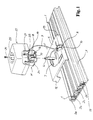
- a voltage rail 1 which can be installed with a wall, in the roof, etc.
- the voltage rail 1 has conducting paths 2a, 2b, 2c and 2d, which are situated parallel to the surface on which the voltage rail 1 is installed said paths having open surfaces in against the voltage rail. Cavities or channels are formed between the conducting paths 2a - 2d and the back wall of the voltage rail. Further there is a path 3 which has ground potential situated next to the voltage rail.
- Signaling paths 11 are, in this example, situated in the voltage rail between the conducting paths 2a - 2d and the ground path 3.
- the circuits of the conducting paths are mixed, so that paths 2a and 2c form one circuit, and 2b and 2d form another circuit.
- a packing body, or "hose” 4 made from a flexible and insulating material, such as rubber, for filling the cavity. This gives the advantage that it is more difficult to accidently gain access to the conducting paths, and it is also protects against corrosion.
- Fig. 1 shows an adapter for an outlet; objects can of course also be connected directly to the rail. For example, it is easy to consider an electric heater or other stationary equipment, which can be connected directly to the rail without an interconnecting cable.
- the adapter comprises a mounting plate 5, which is equipped with lips 12, 13 adapted to make total contact against the voltage rail 1. Furthermore, most adapters of this kind will have a contact 8 for the ground potential path 3 such as a lip 10 to contact against path 3 and a cable 9 or similar providing contact with the ground outlet of the equipment in question, in this case the electric outlet.
- the mounting plate 5 is also equiped with grooves 7 for the net voltage contacts 17 and an upward extending post 6 which functions as a guide for a rotating plate 20 and a electric outlet cover 15.
- An "operative" part 14 of the electric outlet comprises contact elements 16, which have a lower end 17 adapted for making contact against one of the paths 2a - 2d, and an upper end 18 constructed as an "U", having a tapered section to form a strong contact against the protruding plug contacts.
- the upper end 18 is contained in an isolated cover 19 which is cast fixed to the isolating rotating plate 20 of the electric outlet. Ground potential is taken to ground clamps 21 through a cable 9 which is connected to the ground contact 8.
- the cover 15 for the electric outlet contains a cavity 25 having two orifices for the protruding plug contacts.
- the cover 15 is fixed by a screw 24 in the center of the post 6 of the mounting plate 5.
- Figs. 2a - 2b show different steps during installation of the plug.
- the contacts 16 are situated with their downward extending parts 17 into two conducting paths 2a, 2c.
- the flexible packing body 4 will bend away.
- the plug is rotated anti clockwise, to the position shown in Fig. 2b.
- the contact element, or lips 17 are in place and form contact against the conducting paths 2a, 2c.
- Contacts 17 are thus brought into contact with the conducting paths 2a, 2c, in an axial direction.
- FIGs. 3a-g different variations of voltage rails 1 according to present invention are disclosed.
- the conducting paths 2a - 2d and the ground path 3 can be situated in different ways in the rail 1.
- the ground path 3 can be situated in its own channel.
- Signaling paths 11 are best located on one side of the rail, but they can also be situated differently.
- Fig. 3a shows a voltage rail 1 having one cavity for all of the conducting paths 2a - 2d.
- the ground path 3 is separate.
- Figs. 3b - 3e show voltage rails with two cavities for conducting paths 2a - 2d.
- the ground path 3 is situated in the bottom of the voltage rail 1.
- the conducting paths 2a - 2d are situated in the side walls of the channels.
- Fig. 3f and 3g show variations where the conducting paths are situated in three channels, and where Fig. 3g comprises three circuites.
- FIG. 4a - 4f different variations of packing bodies 4 are shown.
- the packing body should have a profile corresponding to the form of the cavity with the conducting paths 2a - 2d.
- Fig. 4a - 4f there are shown variations of packing bodies which fit to voltage rail 1 of Fig. 1, but it should be understood that different profiles can be used for different variations of the voltage rail.
- the packing bodies 4 have the task of making the cavities with the conducting path 2a - 2d tight while at the same time permitting access of the contact elements 16 to the conducting paths 2a - 2d.
- a person skilled in the art will realise which material can be used to achieve these objects.
- Herein are shown some varitions of technical and aestetic solutions.
- Fig. 4a and 4b show packing bodies 4 of a relatively rigid flexible plastics material, and where the packing body 4 in Fig. 4a is open in against the rail 1, while in Fig. 4b it is a closed tube. Furthermore, the body 4 in Fig. 4a has an extension 26 on one of the side walls, to assist in the holding of the packing body in the cavity of the rail 1 shown in Fig. 1.
- Fig. 4c shows a packing body 4 having a section 27 which extends diagonally to a base section 28. This arrangement will be resilient.
- Fig. 4d shows a compact packing body 4 of rubber or syntetic materials having the necessary properties.
- Fig. 4e and 4f shows the packing body 4 with resilient elements, where Fig. 4e has a separate helical spring 29, and Fig. 4f has a zig-zag spring, which can be cast in one piece with the packing body 4.
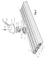
- the plug 31 is constructed so that the "operative" part 14 of the adapter is connected to the cable 32 and situated in an isolating house 15.
- the mounting plate 5 is rotatably connected to the house 15 by the screw 24 being screwed in the guiding post 6.
- On the operative part 14 are situated two sleeves 33.
- In the house 15 are situated two columns (not shown), which fit in the sleeves 33. The columns may thereby assist the transfer of an applied torque from the house 15 to the operative part 14 with contact elements 16.
- the conductors are fixed directly to the contact elements 16, which tongues 17 fits in track 7 of the mounting plate 5.
- the mounting plate 5 is furthermore equipped with ribs 34 on the lower side.
- Fig. 6 Installation of the plug 31 is shown in Fig. 6.
- the contacts 17 are pressed in place against two conducting paths 2a, 2c, so that the packing bodies 4 give in.
- the mounting plate 5 is held against the rail 1 using ribs 34 which fit in the tracks in the grooves of the rail.
- the house 15 with the operative part 14 is rotated as shown with the arrow, and contact is acheived.
- the advantage of this embodiment is that the plug can be connected anywhere along the rail and it is not necessary to use stationary electrical outlets.
Landscapes
- Connector Housings Or Holding Contact Members (AREA)
- Electrical Discharge Machining, Electrochemical Machining, And Combined Machining (AREA)
- Details Of Television Scanning (AREA)
- Electrophonic Musical Instruments (AREA)
- Heat-Pump Type And Storage Water Heaters (AREA)
- Valve Device For Special Equipments (AREA)
- Vehicle Body Suspensions (AREA)
- Magnetic Heads (AREA)
- Laying Of Electric Cables Or Lines Outside (AREA)
- Emergency Protection Circuit Devices (AREA)
- Electric Cable Installation (AREA)
- Machines For Laying And Maintaining Railways (AREA)
- Control Of Vehicles With Linear Motors And Vehicles That Are Magnetically Levitated (AREA)
Applications Claiming Priority (3)
| Application Number | Priority Date | Filing Date | Title |
|---|---|---|---|
| NO921101A NO175078B (no) | 1992-03-20 | 1992-03-20 | Anordning ved strömskinne |
| NO921101 | 1992-03-20 | ||
| PCT/NO1993/000044 WO1993019506A1 (en) | 1992-03-20 | 1993-03-17 | Voltage rail |
Publications (2)
| Publication Number | Publication Date |
|---|---|
| EP0725992A1 EP0725992A1 (en) | 1996-08-14 |
| EP0725992B1 true EP0725992B1 (en) | 1998-08-26 |
Family
ID=19894990
Family Applications (1)
| Application Number | Title | Priority Date | Filing Date |
|---|---|---|---|
| EP93906907A Expired - Lifetime EP0725992B1 (en) | 1992-03-20 | 1993-03-17 | Voltage rail |
Country Status (12)
| Country | Link |
|---|---|
| EP (1) | EP0725992B1 (no) |
| AT (1) | ATE170344T1 (no) |
| AU (1) | AU679174B2 (no) |
| CA (1) | CA2132520A1 (no) |
| DE (1) | DE69320659T2 (no) |
| DK (1) | DK0725992T3 (no) |
| EE (1) | EE9400037A (no) |
| FI (1) | FI944349A0 (no) |
| LT (1) | LT3168B (no) |
| LV (1) | LV10546B (no) |
| NO (1) | NO175078B (no) |
| WO (1) | WO1993019506A1 (no) |
Cited By (3)
| Publication number | Priority date | Publication date | Assignee | Title |
|---|---|---|---|---|
| US10128653B2 (en) | 2009-04-27 | 2018-11-13 | Ideal Industries, Inc. | Low voltage buss system |
| US10186801B2 (en) | 2012-10-03 | 2019-01-22 | Ideal Industries, Inc. | Low voltage buss system |
| WO2023277323A1 (ko) * | 2021-06-28 | 2023-01-05 | 삼성전자 주식회사 | 전원 장치 및 전원 장치에서의 전력 밸런싱 방법 |
Families Citing this family (11)
| Publication number | Priority date | Publication date | Assignee | Title |
|---|---|---|---|---|
| DE4433144A1 (de) * | 1994-09-16 | 1996-03-21 | Kopp Heinrich Ag | Steckdose mit drehbarem Steckereinschubabschnitt |
| DK0787373T3 (da) * | 1994-10-14 | 2002-04-08 | John Ashton Sinclair | Bøjelig elektrisk leder |
| EP0736937A1 (en) * | 1995-04-04 | 1996-10-09 | Atreus Enterprises Limited | Electrical accessory |
| EP0828323A3 (de) * | 1996-08-30 | 1998-12-30 | Siemens Aktiengesellschaft | Sammelschienensystem |
| AUPO222996A0 (en) | 1996-09-10 | 1996-10-03 | Universal Power Track Pty Ltd | An electrical supply assembly |
| EP0862247B1 (de) * | 1997-02-17 | 2006-11-22 | Siemens Aktiengesellschaft | Sammelschienensystem |
| AT411307B (de) * | 2001-09-10 | 2003-11-25 | Konrad Andreas Ing | Mit strom beaufschlagbare leiste |
| ZA200601508B (en) * | 2003-08-21 | 2007-04-25 | Nutek Private Ltd | Electrical power distribution apparatus |
| EA021379B1 (ru) * | 2011-12-29 | 2015-06-30 | Станислав Евгеньевич Буглак | Устройство электрического соединения (варианты) |
| US9912100B2 (en) | 2012-10-03 | 2018-03-06 | Ideal Industries, Inc. | Low voltage buss system |
| RU2601213C2 (ru) * | 2015-03-30 | 2016-10-27 | Виктор Борисович Лебедев | Контактная линия с подвижными штепсельными розетками |
Family Cites Families (9)
| Publication number | Priority date | Publication date | Assignee | Title |
|---|---|---|---|---|
| US2117773A (en) * | 1931-11-23 | 1938-05-17 | Western Union Telegraph Co | Outlet molding |
| CH504119A (de) | 1968-05-28 | 1971-02-28 | Novum Ag | Stromverteileinrichtung |
| CH482329A (de) | 1968-12-06 | 1969-11-30 | Oskar Woertz Inh H & O Woertz | Elektrische Installationseinrichtung mit mindestens einer Stromführungsschiene |
| DE2216145C3 (de) | 1972-04-01 | 1982-07-15 | Staff GmbH & Co KG, 4920 Lemgo | Adapter für Stromschienen |
| IT1062955B (it) | 1976-05-26 | 1985-02-11 | G C Illumination S P A | Canale elettrificato con connettore ad innesto a scatto |
| FI65874C (fi) | 1976-11-19 | 1984-07-10 | Lita | Elmatninganordning |
| DE3048828A1 (de) | 1979-12-29 | 1981-10-01 | Matsushita Electric Works Ltd., Kadoma, Osaka | Stromzufuhrschiene |
| GB2087168B (en) * | 1980-10-28 | 1985-01-30 | Electrak Int Ltd | Electrical distribution system |
| AU6286686A (en) * | 1985-09-05 | 1987-03-24 | Barrier Shelf Co. (No. 27) Pty. Ltd. | Electrical supply rail system |
-
1992
- 1992-03-20 NO NO921101A patent/NO175078B/no not_active IP Right Cessation
-
1993
- 1993-03-17 DE DE69320659T patent/DE69320659T2/de not_active Expired - Fee Related
- 1993-03-17 CA CA002132520A patent/CA2132520A1/en not_active Abandoned
- 1993-03-17 DK DK93906907T patent/DK0725992T3/da active
- 1993-03-17 EP EP93906907A patent/EP0725992B1/en not_active Expired - Lifetime
- 1993-03-17 AU AU37699/93A patent/AU679174B2/en not_active Ceased
- 1993-03-17 AT AT93906907T patent/ATE170344T1/de not_active IP Right Cessation
- 1993-03-17 WO PCT/NO1993/000044 patent/WO1993019506A1/en active IP Right Grant
- 1993-03-18 LV LVP-93-190A patent/LV10546B/xx unknown
- 1993-03-19 LT LTIP434A patent/LT3168B/lt not_active IP Right Cessation
-
1994
- 1994-05-23 EE EE9400037A patent/EE9400037A/xx unknown
- 1994-09-20 FI FI944349A patent/FI944349A0/fi unknown
Cited By (3)
| Publication number | Priority date | Publication date | Assignee | Title |
|---|---|---|---|---|
| US10128653B2 (en) | 2009-04-27 | 2018-11-13 | Ideal Industries, Inc. | Low voltage buss system |
| US10186801B2 (en) | 2012-10-03 | 2019-01-22 | Ideal Industries, Inc. | Low voltage buss system |
| WO2023277323A1 (ko) * | 2021-06-28 | 2023-01-05 | 삼성전자 주식회사 | 전원 장치 및 전원 장치에서의 전력 밸런싱 방법 |
Also Published As
| Publication number | Publication date |
|---|---|
| LV10546B (en) | 1995-04-20 |
| DE69320659D1 (de) | 1998-10-01 |
| WO1993019506A1 (en) | 1993-09-30 |
| AU679174B2 (en) | 1997-06-26 |
| FI944349A (fi) | 1994-09-20 |
| DK0725992T3 (da) | 1999-05-25 |
| NO921101D0 (no) | 1992-03-20 |
| DE69320659T2 (de) | 1999-04-15 |
| NO175078B (no) | 1994-05-16 |
| ATE170344T1 (de) | 1998-09-15 |
| LTIP434A (lt) | 1994-08-25 |
| EP0725992A1 (en) | 1996-08-14 |
| LV10546A (lv) | 1995-02-20 |
| FI944349A0 (fi) | 1994-09-20 |
| NO175078C (no) | 1994-08-24 |
| NO921101L (no) | 1993-09-21 |
| CA2132520A1 (en) | 1993-09-30 |
| EE9400037A (et) | 1995-12-15 |
| AU3769993A (en) | 1993-10-21 |
| LT3168B (en) | 1995-02-27 |
Similar Documents
| Publication | Publication Date | Title |
|---|---|---|
| EP0725992B1 (en) | Voltage rail | |
| US5086194A (en) | Trunking assembly | |
| US8299359B2 (en) | Wiring device and cover plate snap-on assembly | |
| US6265670B1 (en) | Grommet for plurality of cable exits of an enclosure | |
| US4770643A (en) | In-floor fitting | |
| CA2014419C (en) | Interfloor power/communication connection apparatus with debris protection | |
| AU2010357631B2 (en) | Electrical power distribution track system | |
| HU201850B (en) | Channel of rail conductor with connecting device | |
| EP0106535A2 (en) | Electrical track | |
| CA2014420C (en) | Interfloor power/communication connection apparatus | |
| JPS6342385B2 (no) | ||
| FR2453521A1 (fr) | Bloc a barres omnibus | |
| EP0223393A3 (en) | Bulkhead gland assembly | |
| CA2033306C (en) | Protective casing for electric distribution busbars | |
| EP0235206A1 (en) | Electrical supply rail system | |
| DE69926273D1 (de) | Verbindungsvorrichtung für zwei rinnenförmige Leitungen für elektrische Kabelinstallationen | |
| US2283398A (en) | Electric circuit molding | |
| US20030157819A1 (en) | Fabricated baseplate for electrical installations | |
| KR100746787B1 (ko) | 안전 잠금 장치를 구비한 분전함 | |
| WO2000036721A3 (en) | Apparatus for installing flashover protection covers on energized electrical power lines | |
| GB2147152A (en) | Skirting board structure for the distribution of electric energy and other similar services in civil use premises | |
| US20020050553A1 (en) | Mounting device for mounting an electrical device on trunking | |
| AU686077B3 (en) | Electrical outlet device for connection with various types of plugs | |
| JP3232115B2 (ja) | 防雨形ジョイントボックス | |
| US20070042625A1 (en) | Busbar system |
Legal Events
| Date | Code | Title | Description |
|---|---|---|---|
| PUAI | Public reference made under article 153(3) epc to a published international application that has entered the european phase |
Free format text: ORIGINAL CODE: 0009012 |
|
| 17P | Request for examination filed |
Effective date: 19940921 |
|
| AK | Designated contracting states |
Kind code of ref document: A1 Designated state(s): AT BE CH DE DK ES FR GB IE IT LI NL SE |
|
| 17Q | First examination report despatched |
Effective date: 19960930 |
|
| GRAG | Despatch of communication of intention to grant |
Free format text: ORIGINAL CODE: EPIDOS AGRA |
|
| GRAG | Despatch of communication of intention to grant |
Free format text: ORIGINAL CODE: EPIDOS AGRA |
|
| GRAH | Despatch of communication of intention to grant a patent |
Free format text: ORIGINAL CODE: EPIDOS IGRA |
|
| GRAH | Despatch of communication of intention to grant a patent |
Free format text: ORIGINAL CODE: EPIDOS IGRA |
|
| GRAA | (expected) grant |
Free format text: ORIGINAL CODE: 0009210 |
|
| RIN1 | Information on inventor provided before grant (corrected) |
Inventor name: SORENSEN, TORE |
|
| AK | Designated contracting states |
Kind code of ref document: B1 Designated state(s): AT BE CH DE DK ES FR GB IE IT LI NL SE |
|
| PG25 | Lapsed in a contracting state [announced via postgrant information from national office to epo] |
Ref country code: NL Free format text: LAPSE BECAUSE OF FAILURE TO SUBMIT A TRANSLATION OF THE DESCRIPTION OR TO PAY THE FEE WITHIN THE PRESCRIBED TIME-LIMIT Effective date: 19980826 Ref country code: LI Free format text: LAPSE BECAUSE OF FAILURE TO SUBMIT A TRANSLATION OF THE DESCRIPTION OR TO PAY THE FEE WITHIN THE PRESCRIBED TIME-LIMIT Effective date: 19980826 Ref country code: IT Free format text: LAPSE BECAUSE OF FAILURE TO SUBMIT A TRANSLATION OF THE DESCRIPTION OR TO PAY THE FEE WITHIN THE PRESCRIBED TIME-LIMIT;WARNING: LAPSES OF ITALIAN PATENTS WITH EFFECTIVE DATE BEFORE 2007 MAY HAVE OCCURRED AT ANY TIME BEFORE 2007. THE CORRECT EFFECTIVE DATE MAY BE DIFFERENT FROM THE ONE RECORDED. Effective date: 19980826 Ref country code: FR Free format text: LAPSE BECAUSE OF FAILURE TO SUBMIT A TRANSLATION OF THE DESCRIPTION OR TO PAY THE FEE WITHIN THE PRESCRIBED TIME-LIMIT Effective date: 19980826 Ref country code: ES Free format text: THE PATENT HAS BEEN ANNULLED BY A DECISION OF A NATIONAL AUTHORITY Effective date: 19980826 Ref country code: CH Free format text: LAPSE BECAUSE OF FAILURE TO SUBMIT A TRANSLATION OF THE DESCRIPTION OR TO PAY THE FEE WITHIN THE PRESCRIBED TIME-LIMIT Effective date: 19980826 Ref country code: BE Free format text: LAPSE BECAUSE OF FAILURE TO SUBMIT A TRANSLATION OF THE DESCRIPTION OR TO PAY THE FEE WITHIN THE PRESCRIBED TIME-LIMIT Effective date: 19980826 Ref country code: AT Free format text: LAPSE BECAUSE OF FAILURE TO SUBMIT A TRANSLATION OF THE DESCRIPTION OR TO PAY THE FEE WITHIN THE PRESCRIBED TIME-LIMIT Effective date: 19980826 |
|
| REF | Corresponds to: |
Ref document number: 170344 Country of ref document: AT Date of ref document: 19980915 Kind code of ref document: T |
|
| REG | Reference to a national code |
Ref country code: CH Ref legal event code: EP |
|
| REF | Corresponds to: |
Ref document number: 69320659 Country of ref document: DE Date of ref document: 19981001 |
|
| REG | Reference to a national code |
Ref country code: IE Ref legal event code: FG4D |
|
| EN | Fr: translation not filed | ||
| NLV1 | Nl: lapsed or annulled due to failure to fulfill the requirements of art. 29p and 29m of the patents act | ||
| REG | Reference to a national code |
Ref country code: CH Ref legal event code: PL |
|
| PG25 | Lapsed in a contracting state [announced via postgrant information from national office to epo] |
Ref country code: IE Free format text: LAPSE BECAUSE OF NON-PAYMENT OF DUE FEES Effective date: 19990317 |
|
| REG | Reference to a national code |
Ref country code: DK Ref legal event code: T3 |
|
| PLBE | No opposition filed within time limit |
Free format text: ORIGINAL CODE: 0009261 |
|
| STAA | Information on the status of an ep patent application or granted ep patent |
Free format text: STATUS: NO OPPOSITION FILED WITHIN TIME LIMIT |
|
| 26N | No opposition filed | ||
| REG | Reference to a national code |
Ref country code: IE Ref legal event code: MM4A |
|
| PGFP | Annual fee paid to national office [announced via postgrant information from national office to epo] |
Ref country code: GB Payment date: 20000211 Year of fee payment: 8 |
|
| PGFP | Annual fee paid to national office [announced via postgrant information from national office to epo] |
Ref country code: DK Payment date: 20000224 Year of fee payment: 8 Ref country code: DE Payment date: 20000224 Year of fee payment: 8 |
|
| PGFP | Annual fee paid to national office [announced via postgrant information from national office to epo] |
Ref country code: SE Payment date: 20010305 Year of fee payment: 9 |
|
| PG25 | Lapsed in a contracting state [announced via postgrant information from national office to epo] |
Ref country code: GB Free format text: LAPSE BECAUSE OF NON-PAYMENT OF DUE FEES Effective date: 20010317 Ref country code: DK Free format text: LAPSE BECAUSE OF NON-PAYMENT OF DUE FEES Effective date: 20010317 |
|
| GBPC | Gb: european patent ceased through non-payment of renewal fee |
Effective date: 20010317 |
|
| REG | Reference to a national code |
Ref country code: DK Ref legal event code: EBP |
|
| PG25 | Lapsed in a contracting state [announced via postgrant information from national office to epo] |
Ref country code: DE Free format text: LAPSE BECAUSE OF NON-PAYMENT OF DUE FEES Effective date: 20020101 |
|
| PG25 | Lapsed in a contracting state [announced via postgrant information from national office to epo] |
Ref country code: SE Free format text: LAPSE BECAUSE OF NON-PAYMENT OF DUE FEES Effective date: 20020318 |
|
| EUG | Se: european patent has lapsed |
Ref document number: 93906907.6 |