EP0723720B1 - Digitale kommunikationseinrichtung unter verwendung einer vierfachen differenzfrequenzumtastung - Google Patents
Digitale kommunikationseinrichtung unter verwendung einer vierfachen differenzfrequenzumtastung Download PDFInfo
- Publication number
- EP0723720B1 EP0723720B1 EP95900412A EP95900412A EP0723720B1 EP 0723720 B1 EP0723720 B1 EP 0723720B1 EP 95900412 A EP95900412 A EP 95900412A EP 95900412 A EP95900412 A EP 95900412A EP 0723720 B1 EP0723720 B1 EP 0723720B1
- Authority
- EP
- European Patent Office
- Prior art keywords
- signal
- frequency
- bit
- stream
- responsive
- Prior art date
- Legal status (The legal status is an assumption and is not a legal conclusion. Google has not performed a legal analysis and makes no representation as to the accuracy of the status listed.)
- Expired - Lifetime
Links
Images


Classifications
-
- H—ELECTRICITY
- H04—ELECTRIC COMMUNICATION TECHNIQUE
- H04L—TRANSMISSION OF DIGITAL INFORMATION, e.g. TELEGRAPHIC COMMUNICATION
- H04L27/00—Modulated-carrier systems
- H04L27/10—Frequency-modulated carrier systems, i.e. using frequency-shift keying
- H04L27/14—Demodulator circuits; Receiver circuits
- H04L27/144—Demodulator circuits; Receiver circuits with demodulation using spectral properties of the received signal, e.g. by using frequency selective- or frequency sensitive elements
- H04L27/148—Demodulator circuits; Receiver circuits with demodulation using spectral properties of the received signal, e.g. by using frequency selective- or frequency sensitive elements using filters, including PLL-type filters
-
- H—ELECTRICITY
- H04—ELECTRIC COMMUNICATION TECHNIQUE
- H04B—TRANSMISSION
- H04B1/00—Details of transmission systems, not covered by a single one of groups H04B3/00 - H04B13/00; Details of transmission systems not characterised by the medium used for transmission
- H04B1/69—Spread spectrum techniques
- H04B1/713—Spread spectrum techniques using frequency hopping
- H04B1/7156—Arrangements for sequence synchronisation
- H04B2001/71566—Tracking
Definitions
- the present invention relates to digital communications equipment such as digital radio transceivers.
- the invention relates to spread spectrum digital radio transceivers and digital radio transceivers using differentially encoded four state modulation.
- LANs wireless local area networks
- digital radio transceivers are used to link together various computers, which may be mobile or stationary.
- FCC established regulations to allow unlicensed use of certain bands if spread-spectrum techniques are used.
- spread spectrum transmission the energy radiated during radio transmission is spread across a wide spectrum of frequencies and is therefore less liable to cause substantial interference with other radio communications.
- FCC spread-spectrum regulations allow greater transmission power to be used without requiring special licensing, increasing the attainable range of communications for unlicensed systems.
- direct sequencing spreading is achieved through multiplication of the data by a binary pseudo random sequence whose chipping rate is many times the data rate.
- frequency hopping the carrier frequency remains at a given frequency for a duration and then hops to a new frequency somewhere in the spreading bandwidth.
- Direct sequencing allows for coherent demodulation.
- coherent demodulation the receiver exploits knowledge of the carrier wave's phase reference to detect the signals. With frequency hopping, however, phase coherence is difficult to maintain; hence it is usually demodulated non-coherently.
- Non-coherent demodulation refers to demodulation performed with no knowledge of phase, i.e., without phase estimation processing.
- Non-coherent demodulation results in the advantage of reduced complexity over coherent demodulation but at the cost of an increased probability of error.
- Frequency hopping offers other advantages with respect to direct sequence. Frequency hopping enables higher rates to be achieved without requiring very high speed logic that an equivalent direct sequency system would require. Frequency diversity, a technique used to combat multipath fading by transmitting data in multiple frequencies and thus increasing the likelihood that the data will make it through the channel uncorrupted, can be achieved at no additional cost.
- BFSK binary frequency shift keying
- DQPSK differential quadrature phase shift keying
- four information states are defined by changing the phase of a carrier signal in 90° increments.
- DQPSK is therefore a four state modulation scheme, allowing twice the data rate to be achieved through the same channel as compared to two state modulation.
- the carrier phase of the previous signaling interval is used as a phase reference for demodulation. The information is therefore carried by the difference in phase between two successive waveforms.
- two noisy signals are in effect compared with each other. Hence, DQPSK exhibits greater noise but allows for reduced system complexity.
- DQPSK can be demodulated using so-called “differentially coherent” demodulation, which does not require traditional coherent demodulation techniques but still requires more complex (IQ) demodulation.
- DQPSK is a type of phase modulation and as such is vulnerable to phase inversions that are commonly encountered in environments with multipath propagation such as the indoor environment.
- Frequency shift keying (FSK) modulation schemes are generally less costly to implement than phase shift keying (PSK) modulation schemes.
- DQPSK performs better under lower signal-to-noise conditions, it is unsuitable for frequency hopping due to the need to know the carrier phase.
- frequency hopping systems the carrier is always changing frequency, which creates problems in DQPSK systems, since small frequency errors translate into large phase errors.
- operation in multipath indoor environments creates phase reversals of the carrier as a transceiver moves across a null. Phase Shift Keying systems have difficulty dealing with this situation.
- a prior art document, EP-A-0 184 953, describes digital data transmission of numerical information, using differential frequency shift keying of symbols for sampling and fast Fourier transform processing.
- a modulation encoder groups the bits for transmission into symbols, each associated with a frequency shift in accordance with a memory table. The step of frequency is added, in a synthetiser, to the frequency of the preceding symbol if that frequency was below the centre value, and subtracted if the previous frequency was above the centre frequency.
- the received signal is sampled and applied to two FFT processors, whose symbol synchronisation inputs are offset by half a symbol, for demodulation and synchronisation respectively. Spectral lines exceeding an amplitude threshold are selected for demodulation.
- the invention includes a communications transmitter for transmitting a digital bit stream and a communications receiver for receiving a digital bit stream. Combined, the communications transmitter and communications receiver constitute a communications transceiver.
- the present invention is referred to as a differentially encoded, 4-level frequency shift keying (D4FSK) transceiver and in its preferred embodiment provides for digital communications equipment that is low cost, miniaturizable, low in power consumption and high in spectral efficiency.
- D4FSK 4-level frequency shift keying
- a communications transceiver for transmitting and receiving digital information represented as a binary digital bit stream includes circuitry for converting a binary digital bit stream to be transmitted to a stream of multi-bit symbols, circuitry for differentially encoding the stream of multi-bit symbols to produce a stream of differentially encoded symbols, circuitry for frequency modulating a carrier signal in accordance with the differentially encoded symbols so as to represent each differentially encoded symbol by one of multiple frequencies related in number to a number of bits represented in the multi-bit symbols, circuitry for frequency modulating a carrier signal in accordance with the differentially encoded symbols so as to represent each differentially encoded symbol by one of multiple frequencies related in number to a number of bits in the multi-bits symbols, circuitry for frequency demodulating such a modulated carrier, producing a multi-level analog signal at the output of the demodulator where each of the levels correspond to the one of the transmitted frequencies (which in turn corresponds to one of the transmitted symbols), circuitry for converting the demodulated analog multi
- each network node is typically equipped with a digital data transceiver including a digital data transmitter and a digital data receiver. Data is input to the transmitter of one node, where a radio frequency carrier is modulated and propagated to a receiver in another node. The receiver recovers the signal and outputs it as a digital binary data stream.
- a digital data transceiver including a digital data transmitter and a digital data receiver.
- Data is input to the transmitter of one node, where a radio frequency carrier is modulated and propagated to a receiver in another node.
- the receiver recovers the signal and outputs it as a digital binary data stream.
- the present digital data transceiver uses the spread spectrum technique of frequency hopping. It also uses differential quaternary (4-level) frequency shift keying (D4FSK).
- D4FSK differential quaternary (4-level) frequency shift keying
- a serial binary bit stream is arranged into a stream of consecutive bit pairs. For example, the bit stream 100111100100 ... is paired up to form the stream 10,01,11,10,01,00 ....
- the stream of bit pairs is mapped into a symbol stream with each symbol having one of four possible values corresponding to integers 0,1,2 and 3.
- the bit pair stream maps into the symbol stream 1,2,0,1,2,3. Other mapping arrangements are also possible and would work equally well.
- the resulting symbol stream is differentially encoded by performing an addition (modulo 4) of the next symbol generated from the next bit pair with the previous differentially encoded symbol.
- the result is the next differentially encoded symbol to be transmitted.
- the information contained in the bit pairs is therefore carried in the difference between two consecutive differentially encoded symbols instead of the absolute value of a symbol.
- the differentially encoded symbols are then converted to a voltage which is proportional to the numeric value of the symbol and are frequency modulated onto a carrier in any of several commonly available ways.
- the D4FSK receiver looks for the difference between two consecutive frequency-modulated, differentially-encoded symbols to determine which bit pair was transmitted to reconstruct the original bit stream.
- the DFSK scheme can be used for other bit arrangements involving more or less than 2 bits per symbol and is of particular advantage in arrangements with more than one bit per symbol in which the symbols are then frequency modulated and the system is frequency hopped.
- the system is therefore more susceptible to errors caused by frequency perturbations such as frequency noise, frequency drift, frequency distortion, etc.
- frequency hopping systems this is of special importance because the agility requirements placed on the carrier generally result in frequency errors of the kind mentioned above.
- the differential encoding technique described above greatly aids in the detection of the frequency modulated signal by having the receiver remove any component of the signal that does not vary between two consecutive symbols. Therefore, the generation of the hopping carrier can be accomplished with simpler circuitry and lower cost by allowing some errors to be present while achieving accurate signal demodulation and detection.
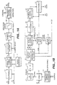
- a clock generator 11 produces a clock and the bit data rate by dividing down a crystal reference frequency.
- the clock generator also produces a clock at the symbol rate, which is one-half the bit rate.
- the symbol clock clocks all circuitry that processes symbols, namely a serial-to-symbol converter, a differential encoder and a symbol to 4FSK converter.
- the bit rate clock, TX_CLOCK is also provided to the serial-to-symbol converter, as well as to a scrambler and to a host device.
- the host device produces transmission data TX_DATA which is input to a scrambler 13.
- the scrambler effectively randomizes the transmission data, therefore maintaining data transitions of all types.
- three-step transitions are required by an adaptive digital slicer for maximum signal value averaging, and two and three-step transitions are required by a phase-lock NCO for clock recovery.
- the scrambler also improves spreading on a given hop channel, and reduces carrier drift in the frequency hopping synthesizer.
- the final bit stream is unscrambled using an inverse algorithm.
- the randomized transmission data is input to a serial-to-symbol converter 15.
- the serial-to-symbol converter simply takes a pair of serial input bits and forms a symbol of two bits in parallel.
- the resulting two-bit symbols are then input to a differential encoder 17.
- a new symbol is summed with the last symbol that was output to form the next symbol to be output using modulo-4 arithmetic.
- a subtractor is used to decode the differentially encoded symbols. Assume for purposes of example that the symbols 00, 01, 10, 11 were to be transmitted in that order.
- the first symbol 00 would be summed with an implied last symbol of 00 using modulo-4 arithmetic producing 00 as the symbol to be output.
- Summing the next symbol 01 with the last symbol 00 produces 01 as the symbol to be output.
- Summing the next symbol 10 with the last symbol 01 produces the symbol 11 to be output.
- summing the next symbol 11 with the last symbol 11 produces the symbol 10 to be output.
- the differentially encoded symbols are then converted to a stair-step voltage signal having four voltage levels in a symbol-to-4FSK converter 19. That is, the symbol-to-4FSK converter converts the symbol (bit pair) that is to be transmitted into voltages that can be used to modulate a frequency hopping synthesizer 21. A highest voltage level is used to represent the symbol 11, a next highest voltage level is used to represent the symbol 10, a next voltage level is used to represent the symbol 01 and a lowest voltage level is used to represent the symbol 00.
- the resulting stair-step voltage waveform is passed through a spectrum shaper 20 to produce a modulation signal for the frequency hopping synthesizer 21, the spectrum shaper ensuring that the resulting RF output signal fits within the required transmission window as previously discussed.
- the scrambler 13 helps spread the spectrum within a given channel
- the main spreading comes by the frequency hopping synthesizer 21 jumping from channel to channel in a specific pattern.
- Different networks may be created by using orthogonal hop sequences.
- a control signal applied to the frequency hopping synthesizer is used to designate a particular hop channel. As the control signal is varied, the frequency hopping synthesizer jumps from channel to channel.
- the spread spectrum radio frequency signal propagated by a radio transmitter such as the radio transmitter of Figure 1a is despread using an identical frequency hopping synthesizer 23 jumping from channel to channel in the same specific pattern as the radio transmitter.
- the frequency hopping synthesizer controls a tuner 25 that is tuned to receive only radio signals within the band of a current hop channel.
- the tuner inputs the radio frequency signal and mixes it with the frequency hopping synthesizer output to despread the signal.
- Despreading therefore takes place before intermediate frequency (IF) filtering and demodulation, with the result that the frequency hop method exhibits inherently better sensitivity than an equivalent direct sequence approach.
- the radio frequency signal output by the transmitter is in the vicinity of 2400 Mhz
- the intermediate frequency signal output by the tuner is in the vicinity of 44 Mhz.
- the IF signal is input to an FM demodulator 27, which converts the frequency state changes into a base band voltage called an "eye" pattern, shown in Figure 7.
- the FM demodulator therefore reproduces the stair-step analog voltage waveform produced in the transmitter by the symbol to 4FSK converter.
- the peak-to-peak voltage of the eye pattern varies with the modulation index of the transmitter and with component tolerances.
- the DC level of the eye pattern varies depending on the frequency drift of the crystal oscillators in both the receiver and the transmitter as well as component variations.
- An A-to-D converter 29 is therefore used to 10 times oversample the incoming eye pattern.
- the oversampling operation produces a digitized FM video signal, i.e., a digital signal in which different signal levels correspond to different ones of the four D4FSK frequencies.
- an analog comparator is used to determine if the data sent is a one or a zero, with a reference voltage being connected to one input of the analog comparator and the FM video signal being connected to the other input of the analog comparator.
- a comparator looks at the FM video to determine if the data sent is a 00, 01, 10, or 11.
- a number of factors render the analog, BFSK type approach unsuitable for use in the present high performance D4FSK system.
- the problem of recovering 4FSK is significantly more difficult than that of BFSK, because the receiver does not have a prior knowledge of where the thresholds should be set.
- the threshold voltages are based on the peak deviation and for the carriers center frequency and therefore must be adaptable.
- To calculate the threshold using analog circuitry the maximum and minimum peaks of the FM video signal must be found and then heavily filtered to produce stable comparison voltages. Such filtering could require milliseconds to settle.
- a fast system by contrast, requires the threshold to stabilize in tens of microseconds.
- the FM video signal exhibits a poor signal to noise ratio such that the threshold voltages must be set very precisely.
- Such precision cannot be achieved with resistors and voltage sources that have relatively poor accuracy tolerances and comparators that have offset voltages and currents.
- an analog system is extremely sensitive to low frequency variations such as carrier drift in the transmitter synthesizer. The synthesizer is therefore required to have a very narrow loop bandwidth when transmitting, increasing its complexity.
- the input signal changes from a noisy input to a received signal input, the DC level of the signal is generally different than the DC level of the noise. This difference creates a large DC transient on the FM video signal that produces erroneous operation of an inexpensive analog comparator.
- reception of D4FSK using an analog approach is impractical if not impossible.
- an adaptive digital slicer 31 of the present D4FSK receiver receives as its input a digitized, oversampled eye pattern (FM video signal) and outputs high, middle and low bits corresponding to which of a high, mid and low threshold value are exceeded by the value of the oversampled FM video signal as shown in the following Table 1.
- the "eye" pattern is oversampled ten times each symbol period, although other oversampling rates are also possible.
- FM Video H M L Symbol low voltage 0 0 0 00 mid 1 0 0 1 01 mid 2 0 1 1 10 high voltage 1 1 1 11
- the adaptive digital slicer block also performs differential decoding and inherently performs a function analogous to automatic frequency control in analog FSK systems.
- the digitized eye pattern is first processed by a differential decoder.
- the differential decoder uses a subtractor to decode the differentially encoded symbol. Since a particular symbol is differentially encoded as the sum of that symbol and the previously transmitted symbol, the same symbol is differentially decoded by subtracting from a voltage value representing the symbol a voltage value representing the previously received symbol. The resulting voltage value is compared to the high, middle and low threshold values computed from an average maximum value of the digitized FM video signal.
- the HML bits are set in accordance with Table 1 and input to a 4FSK-to-symbol converter 33, wherein the bits are converted to the corresponding symbol, also as shown in Table 1. If a sign bit from the differential decoder portion of the slicer block 31 indicates a negative value, then the output of the 4FSK-to-symbol converter is complemented in a 2s complementer 35 to account for the modulo nature of the differential encoding.
- the output of the 2s complementer is a series of symbols identical to the series of symbols input to the differential encoder of the radio transmitter.
- the 4FSK-to-symbol converter and the 2s complementer are clocked by a symbol clock SYM_CLK produced by the phase lock NCO 37 in response to a timing signal derived from the analog eye output signal of the FM demodulator and designated "eye".
- the symbol clock is multiplied by two to produce a receive clock RX_CLK which is input to a symbol-to-serial converter 39 and an unscrambler 41.
- the phase lock NCO also operates in cooperation with a lock detect block 43 to produce a carrier detect signal CD.
- the carrier detect signal is input to the slicer block so as to enable to slicer to operate only after a signal is present. Otherwise, the slicer will find the peak-to-peak voltage of noise present at the RF input which, as will be seen, may lock up the slicer indefinitely. Clock recovery and carrier detection are discussed in greater detail hereinafter.
- the symbol-to-serial converter 39 converts the two-bit symbol output from the 2s complementer into a serial data stream running at twice the symbol rate.
- the unscrambler 41 unscrambles the scrambled data to give an RX_DATA stream identical to the TX_DATA stream.
- the purpose of the described D4FSK modulation is to allow for data recovery in the presence of low frequency noise superimposed on the modulation.
- Low frequency noise is injected into communication systems at a variety of places.
- One source of low frequency noise is carrier drift in the transmitter synthesizer due to a non-zero loop bandwidth in the presence of random FM modulation from the data to be transmitted.
- Another source of low frequency noise is AC coupling capacitors, which can cause large DC swings when the system goes from a no signal (noisy) condition to a signal input condition.
- the eye pattern is undetectable on an oscilloscope at the FM demodulator output. However, once the video signal is digitized and differenced, the differential eye pattern is substantially "clean".
- the benefit of a differential method lies in the fact that signal level difference due to interfering modulation will remain constant over small time periods. Therefore, if the rate of an interfering modulation is much less than the symbol rate, it will not affect the receiver's pattern. For example, if the current symbol is 11 and the previous symbol is 00, then the output of the differential decoder will be the peak-to-peak voltage of the FM video eye pattern. No matter what the absolute DC level of the eye pattern, the peak-to-peak value will still be the same.
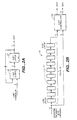
- the transmitter differential encoder 17 of Figure 1a may be realized using a 2 bit adder 45 and a 2 bit latch 47 that receives the output of the 2 bit adder.
- a 2 bit symbol from the serial-to-symbol converter 15 of Figure 1a is input to the 2 bit adder together with the previous output of the 2 bit adder stored in the 2 bit latch.
- the present symbol is added to the previous symbol and output as a differentially encoded symbol.
- the receiver sampling clock 10 times oversamples the incoming eye pattern.
- a chain 50 of 10 latches 51 is used in the receiver differential decoder to subtract the current symbol from the previous symbol as shown in Figure 2b.
- the subtraction is performed by a 6 bit subtractor 53 which produces a 6 bit difference magnitude and a sign bit which is input to the 2's complementer as shown in Figure 1b.
- the difference magnitude output of the 6 bit subtractor is input to the adaptive digital slicer 31 of Figure 1b. More particularly, the output of the differential decoder goes to a peak detector 55.
- the purpose of the peak detector is to output a signal when the difference magnitude is a peak-to-peak voltage value. This peak-to-peak value is needed to calculate the thresholds values used for data slicing.
- the peak detector outputs a pulse when two conditions are satisfied: (a) the difference goes through a maximum, i.e., it goes from a rising edge to a falling edge; and (b) the maximum is greater than the high threshold. This condition ensures that the maximum is a peak-to-peak maximum.
- the peak detector When the peak detector detects a peak-to-peak maximum, it outputs a signal AVG to an averager 57.
- the averager inputs the difference magnitude then present on the difference bus DIFF and combines it with a previously calculated average to arrive at a running average of the maximum peak-to-peak value.
- the average maximum peak-to-peak value, designated MAX_VAL, is input to a threshold computer 59.
- the differential nature of the slicer allows the average to be realized with a very low gate count.
- a non-differential method would require a maximum peak average and a minimum peak average.
- the computation of the thresholds would also be more complicated. Using a differential slicer, the thresholds may be very simply calculated as shown in the following Table 2.
- the difference magnitude is compared to the threshold values input from the threshold computer to produce the H, M and L bits as in Table 1 above.
- the averager of the differential slicer may be realized using a 6 bit subtractor 63, a 7 bit latch 65, a 9 bit adder 67 and a 9 bit latch/mux 69.
- the 6 bit subtractor 63 subtracts the incoming peak-to-peak value from the value stored in the most significant 6 bits of the 9 bit latch 69. If a difference is zero, nothing changes. If the difference is not zero, the difference is added to the contents of the 9 bit latch 67, but the difference is first divided by 8. Therefore, 8 peaks that have an error of +1 are required to move the max register up one. A filtering action results, such that the max value will record the average peak-to-peak value even under heavy noise conditions.
- a fast lock-up circuit enables the receiver to lock up to a received signal in 20us.
- the fast lock-up circuit produces a FAST LOAD signal that is input to the 9 bit latch/mux 69 of the averager. If the incoming peak-to-peak value is very different from the stored value, the slicer assumes that the MAX_REG is wrong and puts the new value directly into the MAX_REG.
- the general approach to clock recovery used in the receiver is to detect and produce a pulse upon the occurrence of two and three step transitions, the resulting pulse train being input to the phase lock NCO 37 of Figure 1b.
- the pulses occur roughly every symbol period. Some of the pulses, however, will be missing (because of noise and because one step transitions are not detected), and the pulses are subject to considerable pulse jitter.
- the function of the phase lock NCO is to extract from the pulse train a clean clock signal.
- the pulse train is produced by the slicer 31 of Figure 1b in a similar manner as the peak detection signal AVG and using partially the same circuitry.
- An output of the seventh latch 51a of the delay 10 shift register is input together with the digitized FM video signal to a 6 bit subtractor 71 separate from but identical to the 6 bit subtractor 53 in Figure 3a.
- the resulting difference signal is input to a peak detector 73 similar to the peak detector 55 in Figure 3a, except that the peak detector 73, instead of detecting only three step transitions, detects two and three step transition.
- the peak detector 73 outputs a substantially regular pulse train "eye".
- FIG 4b shows in greater detail the phase lock NCO and lock detect blocks of Figure 1b.
- the pulse train eye is input to a ping-pong phase detector 75.
- the ping-pong phase detector contains two pipelined phase detectors.
- the pulse train starts a counter (not shown) that computes the time difference between the occurrence of a pulse in the pulse train and the occurrence of a pulse in a feedback signal from a number controlled oscillator 77.
- the number controlled oscillator (NCO) is set to produce as the feedback signal a pulse train having a nominal frequency of 800 Khz. If a new eye pulse occurs before the time difference calculation is finished, the second phase detector will operate on the newly arrived eye pulse.
- the time difference error is represented using a sign bit and three magnitude bits, E0, E1 and E2, all of which are input into a loop bandwidth module 79 and to a carrier detect circuit 81.
- the loop bandwidth module is essentially a gain block that sends a tune number to the NCO. If the error is zero, then the NCO tune number is unity. If the error is greater than zero, the NCO is phase advanced and must be slowed down. A tune number less than one is sent to the NCO for one master clock cycle inducing a small phase shift in the NCO output without changing the frequency of the output. Similarly, if the error is less than zero as indicated by the sign bit, the NCO is phase retarded and must be sped up. A tune number greater than one is therefore sent to the NCO for one master clock cycle.
- the phase-lock NCO is configured as a memoryless loop in that the phase detector output controls the NCO phase, not its frequency. This feature prevents possible overshoot or unstable oscillatory conditions.
- a standard Phase Lock Loop does not use a true phase controlled oscillator but rather it uses a frequency controlled oscillator. Because it tries to control phase by using frequency, this type of loop has an inherent integrator which "remembers" its previous state. Loops containing a memory can overshoot and even go unstable if they are not controlled correctly.
- a carrier detect signal is produced by comparing a radio signal strength indicator (RSSI) measurement to a threshold value. RSSI, however, measures signal strength regardless of the source, whether interfering or non-interfering.
- RSSI radio signal strength indicator
- the present invention uses as a carrier detect circuit a circuit somewhat akin to a bit error estimator in order to ensure that only usable, non-interfering signals are received.
- the magnitude bits E0, E1 and E2 of the phase detector error signal are used together with the eye signal to produce the carrier detect signal.
- the error signal is weighted in a phase error detector block 83. For example, errors of +3 contribute greater weight to an unlocked (no carrier) determination than errors of ⁇ 2, etc.
- the eye signal is examined for sparsity in an eye sparsity detector 85. Because of the stringent rules placed on the input signal for an eye pulse to occur, random noise produces fewer pulses on the eye line than a real signal. Therefore, eye sparsity detection is useful for aiding in determination of an unlock condition. The longer the time between eye pulses, the larger the contribution to the determination of an unlocked condition.
- a sparse eye signal may also be indicative, for example, of an interfering continuous wave signal on the received channel.
- the eye signal will disappear. Normally, this condition would produce a zero error signal, since the phase detect indicates no error if no data is present on the eye signal. However, the eye sparsity detector will show an unmistakable unlock condition and will report correctly that the system is unlocked.
- NOR gate 87 produces a binary low signal that is input to a bit filter 89.
- the raw carrier detect line in a conventional radio receiver is "glitchy". For this reason, the bit filter 89 is needed.
- the input signal from the NOR gate 87 feeds the up/down line of a counter, the MSB of which forms the carrier detect output signal. In the case of the five stage counter, it takes 16 symbol times under high signal to noise ratio conditions for the counter to change from one state to another. Thus the rise time, in an exemplary embodiment, is about 20us, giving a simple digital low pass filter function.
- a transmission header of the radio protocol is designed to facilitate error free operation.
- the phase detector 83, eye sparsity detector 85 and bit filter 89 of the carrier detector are shown in greater detail in Figures 5a, 5b and 5c, respectively.
- the magnitude bits E0, E1 and E2 of the phase detector error signal are weighted so that larger phase errors produce a disproportionally longer unlocked indication than do smaller phase errors. Without weighing, insufficient error information is obtained and the circuit appears to be locked substantially all of the time. Weighing is accomplished using a suitable look-up circuit 101.
- the weighted error signal W[3:0] is input to a three-bit counter 103 whenever it exceeds the value already in the counter 103 as determined by a comparator 105.
- the counter 103 counts down with each symbol clock period. When the counter reaches zero (terminal count, TC), a locked condition is indicated by the phase error detector portion 83 of the carrier detect circuit 81.
- the eye sparsity detector 85 may be realized using a simple four-bit down counter clocked by the symbol clock. Upon each occurrence of an eye pulse, a constant value 1111 is loaded into the counter and then counted down with each symbol clock cycle. So long as the counter does not reach terminal count before a next eye pulse reloads the counter, a locked condition is indicated by the eye sparsity detector portion 85 of the carrier detect circuit 81.
- the output signals of the phase error detector and the eye sparsity detector both indicating a locked condition when their respective output signals are low, are ORed together by the OR gate 87.
- the output of the OR gate 87 is a logic low signal, respective locked conditions as independently detected by the phase error detector and the eye sparsity detector coincide.
- the bit filter 89 eliminates momentary glitches from the output of the OR gate 87.
- the bit filter determines whether the output of the OR gate 87 is mostly high (indicating an unlocked condition) or mostly low (indicating a locked condition).
- the bit filter may be realized using a 5-bit up/down counter 109 and a logic circuit 110 that enables or disables the counter.
- the counter is clocked by the symbol clock and counts down when the input IN is 0 and up when the input IN is 1.
- the most significant bit of the counter forms the output signal OUT of the bit filter.
- the logic circuity 110 includes a circuit 111 that disables the counter if the count (excluding the MSB) is 0000 and the input symbol IN is zero and a circuit 113 that disables the counter if the count (including the MSB) is 11111 and the input signal IN is 1.
- the output signals from the circuits 111 and 113 are Ored together using an OR gate 115 and input to a chip enable input CE of the counter 109.
- the contents of the counter have just been initialized to zero and that the input signal IN indicates an unlocked condition.
- the counter will be disabled and will remain at zero count until the input signal IN dictates a locked condition, at which time the counter will begin to count up.
- the input signal IN must continue to indicate a locked condition for 10000 2 (16 10 ) symbol clock cycles before the MSB of the count is asserted, giving a carrier detect indication. If the input signal IN continues to indicate a locked condition for 15 additional symbol clock cycles, the counter will reach 11111 and be disabled by the logic circuit 13. If a glitch occurs and the input signal IN indicates a temporary unlock condition, the counter will begin to count down, but the MSB will not be affected until the unlock condition has persisted for a given period of time.
- a design of a frequency hopping synthesizer used in both the radio transmitter and the radio receiver facilitates fast frequency hopping while minimizing modulation distortion.
- Fast-frequency transitions require a synthesizer to have a very wide loop bandwidth.
- a loop bandwidth greater than 20 KHz is required.
- FM modulation on the other hand, a very narrow loop bandwidth is required since a wide bandwidth would cause filtering and distortion of the modulation.
- the loop bandwidth should be less than 1 KHz.
- a reference frequency and a divided down feedback signal from a voltage controlled oscillator (VCO, not shown) are input to a digital phase processing block 91 which produces a digital phase error number.
- the digital phase error number is converted to an analog signal and sampled in a sample and hold phase detector 93.
- the sampled analog signal is input to a loop filter 94 comprising two op-amps, one (95) at the loop filter input and another (97) at the loop filter output.
- the output of the first op-amp 95 is fed back directly to the inverting input of the op-amp.
- the output is also connected through a series combination of two resistors to the inverting input of the second op-amp filter 97.
- One of the series connected resistors, R 1 may be bypassed by controlling a field effect transistor (FET) Q 1 .
- FET field effect transistor
- a bandwidth control signal BW control feeds a bipolar transistor and associated bias resistors in order to turn FET Q 1 on, effectively removing the resistor R 1 from the circuit, or off, allowing the resistor R 1 to remain in the circuit.
- the non-inverting input of the second op-amp filter 97 is connected to a reference voltage (+2V).
- the op-amp output is connected through the series combination of two resistors and a capacitor back to the inverting input.
- One of the series resistors, R 2 may be bypassed by a second FET Q 2 with its associated bipolar transistor and bias resistors.
- the output of the second op-amp filter passes through a resistor to produce a VCO TUNE output.
- a modulation input is connected through another resistor to the VCO TUNE output to effect modulation.
Claims (25)
- Kommunikationssender zum Senden eines digitalen Bitstroms mit einer Einrichtung (15) zum Umwandeln des digitalen Bitstroms in einen Strom von Mehrfach-Bit-Symbolen, dadurch gekennzeichnet, daß der Sender folgendes aufweist:eine Einrichtung (17) zum differentiellen Codieren des Stroms von Mehrfach-Bit-Symbolen, um einen Strom von differentiell codierten Symbolen zu erzeugen; undeine Einrichtung (19) zum Frequenzmodulieren eines Trägersignals gemäß den differentiell codierten Symbolen, um jedes differentiell codierte Symbol durch eine einer Vielzahl von Frequenzen darzustellen, die anzahlmäßig auf eine Anzahl von Bits in den Mehrfach-Bit-Symbolen bezogen sind.
- Vorrichtung nach Anspruch 1, wobei die Anzahl von Frequenzen wenigstens vier ist.
- Kommunikationsempfänger zum Empfangen eines digitalen Bitstroms, der durch Bilden von Mehrfach-Bit-Symbolen und differentielles Codieren aufeinanderfolgender Paare der Mehrfach-Bit-Symbole codiert ist, um differentiell codierte Symbole zu erzeugen, und frequenzmoduliert ist, um jedes differentiell codierte Symbol durch eine Frequenz aus einer Vielzahl von Frequenzen darzustellen, die anzahlmäßig auf eine Anzahl von Bits der Mehrfach-Bit-Symbole bezogen sind, dadurch gekennzeichnet, daß der Empfänger folgendes aufweist:eine Einrichtung (27) zum Erzeugen eines demodulierten FM-Signals, in welchem unterschiedliche Signalpegel unterschiedlichen Frequenzen aus der Vielzahl von Frequenzen entsprechen, in Antwort auf ein analoges Radiofrequenz-Eingangssignal;eine Einrichtung (29, 31), die auf das demodulierte FM-Signal antwortet, zum adaptiven Bestimmen einer Vielzahl von Signalpegelschwellen, die unterschiedlichen Frequenzen aus der Vielzahl von Frequenzen entsprechen, und zum Vergleichen des demodulierten FM-Signals mit den Schwellen, um zu bestimmen, welches bestimmte Symbol gerade empfangen wird, und um ein Signal zu erzeugen, das dieses anzeigt;eine Einrichtung (33), die auf das Signal antwortet, zum differentiellen Decodieren des Signals in einen Strom von Mehrfach-Bit-Symbolen; undeine Einrichtung (39), die auf den Strom von Mehrfach-Bit-Symbolen antwortet, zum Erzeugen des digitalen Bitstroms.
- Vorrichtung nach Anspruch 3, wobei die Anzahl von Frequenzen wenigstens vier ist.
- Kommunikationstransceiver zum Senden und Empfangen digitaler Information, die als digitaler Bitstrom dargestellt ist, mit einer Einrichtung (15) zum Umwandeln eines zu sendenden digitalen Bitstroms in einen Strom von Mehrfach-Bit-Symbolen, dadurch gekennzeichnet, daß der Transceiver folgendes aufweist:eine Einrichtung (17) zum differentiellen Codieren des Stroms von Mehrfach-Bit-Symbolen, um einen Strom von differentiell codierten Symbolen zu erzeugen;eine Einrichtung (19) zum Frequenzmodulieren eines Trägersignals gemäß den differentiell codierten Symbolen, um jedes differentiell codierte Symbol durch eine Frequenz aus einer Vielzahl von Frequenzen darzustellen, die anzahlmäßig auf eine Anzahl von Bits in den Mehrfach-Bit-Symbolen bezogen sind;eine Einrichtung (27) zum Erzeugen eines demodulierten Signals, in welchem unterschiedliche Signalpegel unterschiedlichen Frequenzen aus der Vielzahl von Frequenzen entsprechen, in Antwort auf ein analoges Radiofrequenz-Eingangssignal;eine Einrichtung (29, 31), die auf das demodulierte FM-Signal antwortet, zum adaptiven Bestimmen einer Vielzahl von Signalpegelschwellen, die unterschiedlichen Frequenzen aus der Vielzahl von Frequenzen entsprechen, und zum Vergleichen des demodulierten FM-Signals mit den Schwellen, um zu bestimmen, welches bestimmte Symbol gerade empfangen wird, und um ein Signal zu erzeugen, das dieses anzeigt;eine Einrichtung (33), die auf das Signal antwortet, zum differentiellen Decodieren des Signals in einen Strom von Mehrfach-Bit-Symbolen; undeine Einrichtung (39), die auf den Strom von Mehrfach-Bit-Symbolen antwortet, zum Erzeugen eines empfangenen Bitstroms.
- Vorrichtung nach Anspruch 5, wobei die Anzahl von Frequenzen wenigstens vier ist.
- Vorrichtung nach Anspruch 6, wobei der Transceiver ein D4FSK-Codieren/Modulieren verwendet.
- Vorrichtung nach Anspruch 6, wobei die Einrichtung (29, 31) zum adaptiven Bestimmen der Vielzahl von Signalpegelschwellen eine Einrichtung (55, 57) zum Bestimmen eines mittleren Spitzenwerts des demodulierten FM-Signals und eine Einrichtung (59) zum arithmetischen Berechnen der Vielzahl von Signalpegelschwellen aus dem mittleren Spitzenwert aufweist.
- Vorrichtung nach Anspruch 6, wobei der Transceiver ein Frequenzsprungverfahren verwendet und weiterhin folgendes aufweist:eine erste Frequenzsprungverfahrens-Synthesizereinrichtung (21), die auf ein erstes Steuersignal antwortet, zum Variieren einer Sende-Mittenfrequenz des Trägersignals in einem vorbestimmten Muster; undeine zweite Frequenzsprungverfahrens-Synthesizereinrichtung (23), die auf ein zweites Steuersignal antwortet, zum Variieren einer Empfangs-Mittenfrequenz in einem vorbestimmten Muster.
- Vorrichtung nach Anspruch 9, wobei der erste und der zweite Frequenzsprungverfahrens-Synthesizer (21, 23) jeweils einen Phasenregelkreis aufweist, der folgendes aufweist:einen spannungsgesteuerten Oszillator;eine Referenzfrequenzquelle;einen Phasendetektor (93), der mit der Referenzfrequenzquelle und mit einem frequenzgeteilten Ausgang des spannungsgesteuerten Oszillators verbunden ist; undein Kreisfilter (94), das mit dem Phasendetektor und dem spannungsgesteuerten Oszillator verbunden ist und zwischen einer breiten Bandbreite für ein agiles Frequenzsprungverfahren und einer schmalen Bandbreite für eine Frequenzstabilität zwischen Sprüngen umschaltbar ist.
- Vorrichtung nach Anspruch 10, wobei das Kreisfilter ein aktives Operationsverstärker-Kreisfilter aufweist.
- Vorrichtung nach Anspruch 11, wobei das aktive Operationsverstärker-Kreisfilter folgendes aufweist:einen Operationsverstärker;eine Spannungsquelle, die mit einem ersten Eingangsanschluß des Operationsverstärkers verbunden ist;einen variablen Widerstand, der mit einem zweiten Eingangsanschluß des Operationsverstärkers und mit einem Signal, das proportional zu einer Phasendifferenz zwischen der Referenzfrequenz und dem Rückkoppelsignal ist, verbunden ist; unddie Reihenschaltung eines variablen Widerstandes und eines Kondensators, die zwischen einem Ausgangsanschluß des Operationsverstärkers und dem zweiten Eingangsanschluß angeschlossen sind, wobei ein am Ausgangsanschluß erzeugtes Signal dazu verwendet wird, den spannungesteuerten Oszillator abzustimmen.
- Vorrichtung nach Anspruch 6, wobei die Einrichtung zum Erzeugen eines demodulierten FM-Signals folgendes aufweist:einen Tuner zum selektiven Empfangen eines Teils des analogen Radiofrequenz-Eingangssignals innerhalb eines Frequenzbands, das um eine Empfangs-Mittenfrequenz zentriert ist;eine Einrichtung, die auf den Teil des analogen Radiofrequenz-Eingangssignals antwortet, zum Erzeugen eines analogen FM-Signals, wobei unterschiedliche Signalpegel unterschiedlichen Frequenzen aus der Vielzahl von Frequenzen entsprechen; undeine Einrichtung zum Abtasten des analogen FM-Signals, um das demodulierte FM-Signal zu erzeugen.
- Vorrichtung nach Anspruch 13, wobei die Einrichtung zum Abtasten das analoge FM-Signal mit irgendeinem Multiplikator einer Überabtastung unterzieht.
- Vorrichtung nach Anspruch 14, wobei der Multiplikator wenigstens zehn ist.
- Vorrichtung nach Anspruch 13, die weiterhin eine Taktwiedergewinnungseinrichtung, die auf das demodulierte FM-Signal antwortet, zum Erzeugen eines mit einer empfangenen Symbolrate synchronisierten Taktsignals aufweist.
- Vorrichtung nach Anspruch 16, wobei die Taktwiedergewinnungseinrichtung einen Phasenregelkreis aufweist, der eine Phasenerfassungseinrichtung enthält.
- Vorrichtung nach Anspruch 17, wobei der Phasenregelkreis einen zahlengesteuerten Oszillator enthält.
- Vorrichtung nach Anspruch 17, wobei die Taktwiedergewinnungseinrichtung eine Einrichtung aufweist, die auf das demodulierte FM-Signal antwortet, zum Erfassen von Übergängen im demodulierten FM-Signal und zum Ausgeben eines Impulses an den Phasenregelkreis beim Auftreten der Übergänge.
- Vorrichtung nach Anspruch 19, wobei die Einrichtung zum Erfassen von Übergängen nur Übergänge erfaßt, die größer als einstufige Übergänge sind.
- Vorrichtung nach Anspruch 19, die weiterhin folgendes aufweist:eine Einrichtung, die auf eine Phasendifferenzausgabe der Phasenerfassungseinrichtung antwortet, zum Erzeugen eines ersten Signals, das einen Zustand einer Verriegelung/Entriegelung der Taktwiedergewinnungseinrichtung in bezug auf das analoge Radiofrequenz-Eingangssignal anzeigt;eine Einrichtung, die auf die Einrichtung zum Erfassen von Übergängen antwortet, zum Erzeugen eines zweiten Signals, das einen Zustand einer Verriegelung/Entriegelung der Taktwiedergewinnungseinrichtung anzeigt; undeine Einrichtung zum logischen Verknüpfen des ersten und des zweiten Signals, um ein drittes Signal zu erzeugen, das einen Zustand einer Verriegelung/Entriegelung der Taktwiedergewinnungseinrichtung in bezug auf das analoge Radiofrequenz-Eingangssignal anzeigt.
- Vorrichtung nach Anspruch 21, wobei das dritte Signal ein digitales Ein-Bit-Signal ist.
- Vorrichtung nach Anspruch 22, die weiterhin eine Bit-Filtereinrichtung zum Filtern des dritten Signals aufweist, um ein Endsignal zu erzeugen, das einen Zustand einer Verriegelung/Entriegelung der Taktwiedergewinnungseinrichtung in bezug auf das analoge Radiofrequenz-Eingangssignal anzeigt.
- Vorrichtung nach Anspruch 23, wobei die Bit-Filtereinrichtung einen Aufwärts/Abwärts-Zähler aufweist, der durch das Taktsignal getaktet wird und auf einen logischen Zustand des dritten Signals antwortet, um in einer ersten Richtung zu zählen, und auf einen entgegengesetzten logischen Zustand des dritten Signals antwortet, um in einer entgegengesetzten Richtung zu zählen, und wobei ein höchstwertiges ausgegebenes Bit des Zählers das Endsignal liefert.
- Vorrichtung nach Anspruch 24, die weiterhin eine Einrichtung, die auf das dritte Signal und eine ausgegebene Zahl des Zählers antwortet, zum selektiven Sperren des Zählers aufweist.
Applications Claiming Priority (3)
| Application Number | Priority Date | Filing Date | Title |
|---|---|---|---|
| US08/136,749 US5412687A (en) | 1993-10-15 | 1993-10-15 | Digital communications equipment using differential quaternary frequency shift keying |
| US136749 | 1993-10-15 | ||
| PCT/US1994/012184 WO1995010893A1 (en) | 1993-10-15 | 1994-10-17 | Digital communications equipment using differential quaternary frequency shift keying |
Publications (3)
| Publication Number | Publication Date |
|---|---|
| EP0723720A1 EP0723720A1 (de) | 1996-07-31 |
| EP0723720A4 EP0723720A4 (de) | 2000-07-05 |
| EP0723720B1 true EP0723720B1 (de) | 2002-01-30 |
Family
ID=22474200
Family Applications (1)
| Application Number | Title | Priority Date | Filing Date |
|---|---|---|---|
| EP95900412A Expired - Lifetime EP0723720B1 (de) | 1993-10-15 | 1994-10-17 | Digitale kommunikationseinrichtung unter verwendung einer vierfachen differenzfrequenzumtastung |
Country Status (9)
| Country | Link |
|---|---|
| US (1) | US5412687A (de) |
| EP (1) | EP0723720B1 (de) |
| JP (1) | JPH09505700A (de) |
| CN (1) | CN1074215C (de) |
| AT (1) | ATE212769T1 (de) |
| AU (1) | AU681205B2 (de) |
| CA (1) | CA2174142A1 (de) |
| DE (1) | DE69429779T2 (de) |
| WO (1) | WO1995010893A1 (de) |
Families Citing this family (111)
| Publication number | Priority date | Publication date | Assignee | Title |
|---|---|---|---|---|
| IL105180A (en) * | 1993-03-28 | 1998-01-04 | Israel State | Fast frequency code |
| US5526381A (en) * | 1994-05-12 | 1996-06-11 | At&T Corp. | Robust non-coherent detector for π/4-DQPSK signals |
| FR2727813B1 (fr) * | 1994-12-02 | 1997-01-10 | Alcatel Telspace | Dispositif de detection de presence ou d'absence d'une porteuse modulee en numerique, recepteur et procede correspondants |
| CA2195453A1 (en) * | 1995-05-19 | 1996-11-21 | David L. Herrick | Method for spread spectrum communications |
| EP0748093A1 (de) * | 1995-06-08 | 1996-12-11 | Laboratoires D'electronique Philips S.A.S. | Digitales Übertragungssystem mit Entscheidungsmitteln zur Auswahl der Synchronisierungsart |
| US5625645A (en) * | 1995-07-25 | 1997-04-29 | International Business Machines Corporation | Differential pulse encoding and decoding for binary data transmissions |
| EP0795976A3 (de) * | 1996-03-13 | 2000-02-02 | Ascom Tech Ag | Verfahren zum Empfangen eines nach einem ETS-HIPERLAN-Standard kodierten und modulierten Signals |
| US5901171A (en) * | 1996-03-15 | 1999-05-04 | Sirf Technology, Inc. | Triple multiplexing spread spectrum receiver |
| US6041280A (en) * | 1996-03-15 | 2000-03-21 | Sirf Technology, Inc. | GPS car navigation system |
| US6393046B1 (en) | 1996-04-25 | 2002-05-21 | Sirf Technology, Inc. | Spread spectrum receiver with multi-bit correlator |
| US5897605A (en) * | 1996-03-15 | 1999-04-27 | Sirf Technology, Inc. | Spread spectrum receiver with fast signal reacquisition |
| US6125325A (en) | 1996-04-25 | 2000-09-26 | Sirf Technology, Inc. | GPS receiver with cross-track hold |
| US6047017A (en) * | 1996-04-25 | 2000-04-04 | Cahn; Charles R. | Spread spectrum receiver with multi-path cancellation |
| US6018704A (en) * | 1996-04-25 | 2000-01-25 | Sirf Tech Inc | GPS receiver |
| US6198765B1 (en) | 1996-04-25 | 2001-03-06 | Sirf Technologies, Inc. | Spread spectrum receiver with multi-path correction |
| US6917644B2 (en) * | 1996-04-25 | 2005-07-12 | Sirf Technology, Inc. | Spread spectrum receiver with multi-path correction |
| US5859664A (en) * | 1997-01-31 | 1999-01-12 | Ericsson Inc. | Method and apparatus for line or frame-synchronous frequency hopping of video transmissions |
| US6249542B1 (en) | 1997-03-28 | 2001-06-19 | Sirf Technology, Inc. | Multipath processing for GPS receivers |
| US7184426B2 (en) * | 2002-12-12 | 2007-02-27 | Qualcomm, Incorporated | Method and apparatus for burst pilot for a time division multiplex system |
| US6574211B2 (en) * | 1997-11-03 | 2003-06-03 | Qualcomm Incorporated | Method and apparatus for high rate packet data transmission |
| US9118387B2 (en) | 1997-11-03 | 2015-08-25 | Qualcomm Incorporated | Pilot reference transmission for a wireless communication system |
| FI105750B (fi) * | 1997-12-11 | 2000-09-29 | Nokia Networks Oy | Menetelmä ja järjestely signaalin moduloimiseksi |
| US6018547A (en) * | 1998-01-09 | 2000-01-25 | Bsd Broadband, N.V. | Method and apparatus for increasing spectral efficiency of CDMA systems using direct sequence spread spectrum signals |
| US6577684B1 (en) * | 1998-04-07 | 2003-06-10 | Matsushita Electric Industrial Co., Ltd. | Transmission/reception method and device where information is encoded and decoded according to rules defined based on a relation between a previously-generated multilevel code and a currently generated multilevel |
| US6501841B1 (en) * | 1998-12-17 | 2002-12-31 | Intel Corporation | Method for providing security for a transmission of information through a plurality of frequency orthogonal subchannels |
| US6859504B1 (en) | 1999-06-29 | 2005-02-22 | Sharp Laboratories Of America, Inc. | Rapid settling automatic gain control with minimal signal distortion |
| US6505037B1 (en) * | 1999-06-29 | 2003-01-07 | Sharp Laboratories Of America, Inc. | Data unit detection including antenna diversity |
| US8064409B1 (en) | 1999-08-25 | 2011-11-22 | Qualcomm Incorporated | Method and apparatus using a multi-carrier forward link in a wireless communication system |
| AU7724800A (en) | 1999-09-27 | 2001-04-30 | Parthus Technologies Plc | Method and apparatus for in the field wireless device calibration |
| US6621804B1 (en) | 1999-10-07 | 2003-09-16 | Qualcomm Incorporated | Method and apparatus for predicting favored supplemental channel transmission slots using transmission power measurements of a fundamental channel |
| DE19954897A1 (de) * | 1999-11-15 | 2001-07-26 | Infineon Technologies Ag | Verfahren zur Verwendung eines auf Frequenzmodulation basierenden Transceivers für mit einem Spreizspektrumverfahren kodierte Signale |
| US6282231B1 (en) * | 1999-12-14 | 2001-08-28 | Sirf Technology, Inc. | Strong signal cancellation to enhance processing of weak spread spectrum signal |
| US7260620B1 (en) | 2000-01-05 | 2007-08-21 | Cisco Technology, Inc. | System for selecting the operating frequency of a communication device in a wireless network |
| US6732163B1 (en) | 2000-01-05 | 2004-05-04 | Cisco Technology, Inc. | System for selecting the operating frequency of a communication device in a wireless network |
| US6931051B2 (en) * | 2000-03-01 | 2005-08-16 | Texas Instruments Incorporated | Frequency hopping wireless communication system with filtered adaptive slicer |
| US6674818B1 (en) | 2000-04-17 | 2004-01-06 | Rf Micro Devices, Inc. | Reduced complexity decision circuitry |
| US6693954B1 (en) | 2000-04-17 | 2004-02-17 | Rf Micro Devices, Inc. | Apparatus and method of early-late symbol tracking for a complementary code keying receiver |
| US6661834B1 (en) | 2000-04-17 | 2003-12-09 | Rf Micro Devices, Inc. | Carrier recovery for spread spectrum communications |
| US7068683B1 (en) * | 2000-10-25 | 2006-06-27 | Qualcomm, Incorporated | Method and apparatus for high rate packet data and low delay data transmissions |
| US6973098B1 (en) | 2000-10-25 | 2005-12-06 | Qualcomm, Incorporated | Method and apparatus for determining a data rate in a high rate packet data wireless communications system |
| KR100395745B1 (ko) * | 2001-05-16 | 2003-08-27 | 주식회사 젤라인 | 전력선 통신시스템의 다중 채널 주파수 시프트 키잉변복조장치 |
| US20020177446A1 (en) * | 2001-05-23 | 2002-11-28 | Alex Bugeja | System and method for providing variable transmission bandwidth over communications channels |
| US6751250B2 (en) | 2001-05-24 | 2004-06-15 | Proxim Corporation | High-data-rate frequency-hopping wireless communication system |
| JP3882673B2 (ja) * | 2002-05-01 | 2007-02-21 | 双葉電子工業株式会社 | 4値fsk変調方式 |
| SG128432A1 (en) * | 2002-09-04 | 2007-01-30 | Winedge & Wireless Pte Ltd | Apparatus and method for modulating digital data |
| GB0310270D0 (en) * | 2003-05-03 | 2003-06-11 | Univ Edinburgh | Biomolecular devices |
| US20110064214A1 (en) * | 2003-09-09 | 2011-03-17 | Ternarylogic Llc | Methods and Apparatus in Alternate Finite Field Based Coders and Decoders |
| US7505589B2 (en) * | 2003-09-09 | 2009-03-17 | Temarylogic, Llc | Ternary and higher multi-value digital scramblers/descramblers |
| US20070110229A1 (en) * | 2004-02-25 | 2007-05-17 | Ternarylogic, Llc | Ternary and Multi-Value Digital Signal Scramblers, Descramblers and Sequence of Generators |
| US8577026B2 (en) | 2010-12-29 | 2013-11-05 | Ternarylogic Llc | Methods and apparatus in alternate finite field based coders and decoders |
| US7643632B2 (en) * | 2004-02-25 | 2010-01-05 | Ternarylogic Llc | Ternary and multi-value digital signal scramblers, descramblers and sequence generators |
| US7218144B2 (en) * | 2004-02-25 | 2007-05-15 | Ternarylogic Llc | Single and composite binary and multi-valued logic functions from gates and inverters |
| US7696785B2 (en) * | 2004-02-25 | 2010-04-13 | Ternarylogic Llc | Implementing logic functions with non-magnitude based physical phenomena |
| US8374289B2 (en) | 2004-02-25 | 2013-02-12 | Ternarylogic Llc | Generation and detection of non-binary digital sequences |
| US7580472B2 (en) * | 2004-02-25 | 2009-08-25 | Ternarylogic Llc | Generation and detection of non-binary digital sequences |
| US7548092B2 (en) | 2004-02-25 | 2009-06-16 | Ternarylogic Llc | Implementing logic functions with non-magnitude based physical phenomena |
| US20060021003A1 (en) * | 2004-06-23 | 2006-01-26 | Janus Software, Inc | Biometric authentication system |
| US20060029152A1 (en) * | 2004-08-03 | 2006-02-09 | General Dynamics Decision Systems, Inc. | Digital communications transmitter with synthesizer-controlled modulation and method therefor |
| US7562106B2 (en) * | 2004-08-07 | 2009-07-14 | Ternarylogic Llc | Multi-value digital calculating circuits, including multipliers |
| US20100164548A1 (en) * | 2004-09-08 | 2010-07-01 | Ternarylogic Llc | Implementing Logic Functions With Non-Magnitude Based Physical Phenomena |
| US7672416B2 (en) * | 2005-03-30 | 2010-03-02 | Alcatel-Lucent Usa Inc. | High-speed serial transceiver with sub-nominal rate operating mode |
| US7835468B2 (en) * | 2006-03-13 | 2010-11-16 | Silicon Laboratories, Inc. | Impulse detection and reduction in a frequency modulation radio receiver |
| KR100811170B1 (ko) * | 2006-06-28 | 2008-03-07 | 엔에이치엔(주) | 바이럴 트래킹 및 과금 방법과 상기 방법을 수행하는바이럴 시스템 |
| DE102007002230A1 (de) * | 2007-01-10 | 2008-07-17 | Benecke-Kaliko Ag | Thermoplastische Folie |
| US8312551B2 (en) * | 2007-02-15 | 2012-11-13 | Harris Corporation | Low level sequence as an anti-tamper Mechanism |
| US7937427B2 (en) * | 2007-04-19 | 2011-05-03 | Harris Corporation | Digital generation of a chaotic numerical sequence |
| US8611530B2 (en) * | 2007-05-22 | 2013-12-17 | Harris Corporation | Encryption via induced unweighted errors |
| US7921145B2 (en) * | 2007-05-22 | 2011-04-05 | Harris Corporation | Extending a repetition period of a random sequence |
| US7995757B2 (en) * | 2007-05-31 | 2011-08-09 | Harris Corporation | Closed galois field combination |
| US7962540B2 (en) * | 2007-06-07 | 2011-06-14 | Harris Corporation | Mixed radix number generator with chosen statistical artifacts |
| US7974413B2 (en) * | 2007-06-07 | 2011-07-05 | Harris Corporation | Spread spectrum communications system and method utilizing chaotic sequence |
| US7970809B2 (en) * | 2007-06-07 | 2011-06-28 | Harris Corporation | Mixed radix conversion with a priori defined statistical artifacts |
| US7596461B2 (en) * | 2007-07-06 | 2009-09-29 | Cisco Technology, Inc. | Measurement of air quality in wireless networks |
| US8005221B2 (en) * | 2007-08-01 | 2011-08-23 | Harris Corporation | Chaotic spread spectrum communications system receiver |
| US7995749B2 (en) * | 2007-10-30 | 2011-08-09 | Harris Corporation | Cryptographic system configured for extending a repetition period of a random sequence |
| US8180055B2 (en) * | 2008-02-05 | 2012-05-15 | Harris Corporation | Cryptographic system incorporating a digitally generated chaotic numerical sequence |
| US8363830B2 (en) * | 2008-02-07 | 2013-01-29 | Harris Corporation | Cryptographic system configured to perform a mixed radix conversion with a priori defined statistical artifacts |
| US8040937B2 (en) * | 2008-03-26 | 2011-10-18 | Harris Corporation | Selective noise cancellation of a spread spectrum signal |
| US8139764B2 (en) * | 2008-05-06 | 2012-03-20 | Harris Corporation | Closed galois field cryptographic system |
| US8320557B2 (en) * | 2008-05-08 | 2012-11-27 | Harris Corporation | Cryptographic system including a mixed radix number generator with chosen statistical artifacts |
| US8145692B2 (en) * | 2008-05-29 | 2012-03-27 | Harris Corporation | Digital generation of an accelerated or decelerated chaotic numerical sequence |
| US8064552B2 (en) * | 2008-06-02 | 2011-11-22 | Harris Corporation | Adaptive correlation |
| US8068571B2 (en) * | 2008-06-12 | 2011-11-29 | Harris Corporation | Featureless coherent chaotic amplitude modulation |
| US8325702B2 (en) | 2008-08-29 | 2012-12-04 | Harris Corporation | Multi-tier ad-hoc network in which at least two types of non-interfering waveforms are communicated during a timeslot |
| US8165065B2 (en) | 2008-10-09 | 2012-04-24 | Harris Corporation | Ad-hoc network acquisition using chaotic sequence spread waveform |
| US8351484B2 (en) * | 2008-12-29 | 2013-01-08 | Harris Corporation | Communications system employing chaotic spreading codes with static offsets |
| US8406276B2 (en) * | 2008-12-29 | 2013-03-26 | Harris Corporation | Communications system employing orthogonal chaotic spreading codes |
| US8305971B2 (en) * | 2009-01-13 | 2012-11-06 | Cisco Technology, Inc. | Utilizing persistent interference information for radio channel selection |
| US8457077B2 (en) * | 2009-03-03 | 2013-06-04 | Harris Corporation | Communications system employing orthogonal chaotic spreading codes |
| US8437721B2 (en) * | 2009-04-26 | 2013-05-07 | Qualcomm Incorporated | Jammer detection based adaptive PLL bandwidth adjustment in FM receiver |
| US8509284B2 (en) * | 2009-06-08 | 2013-08-13 | Harris Corporation | Symbol duration dithering for secured chaotic communications |
| US8428102B2 (en) * | 2009-06-08 | 2013-04-23 | Harris Corporation | Continuous time chaos dithering |
| US8428103B2 (en) * | 2009-06-10 | 2013-04-23 | Harris Corporation | Discrete time chaos dithering |
| US8340295B2 (en) | 2009-07-01 | 2012-12-25 | Harris Corporation | High-speed cryptographic system using chaotic sequences |
| US8363700B2 (en) | 2009-07-01 | 2013-01-29 | Harris Corporation | Rake receiver for spread spectrum chaotic communications systems |
| US8369376B2 (en) * | 2009-07-01 | 2013-02-05 | Harris Corporation | Bit error rate reduction in chaotic communications |
| US8385385B2 (en) * | 2009-07-01 | 2013-02-26 | Harris Corporation | Permission-based secure multiple access communication systems |
| US8406352B2 (en) * | 2009-07-01 | 2013-03-26 | Harris Corporation | Symbol estimation for chaotic spread spectrum signal |
| US8428104B2 (en) | 2009-07-01 | 2013-04-23 | Harris Corporation | Permission-based multiple access communications systems |
| US8379689B2 (en) * | 2009-07-01 | 2013-02-19 | Harris Corporation | Anti-jam communications having selectively variable peak-to-average power ratio including a chaotic constant amplitude zero autocorrelation waveform |
| US8369377B2 (en) * | 2009-07-22 | 2013-02-05 | Harris Corporation | Adaptive link communications using adaptive chaotic spread waveform |
| US8848909B2 (en) | 2009-07-22 | 2014-09-30 | Harris Corporation | Permission-based TDMA chaotic communication systems |
| US8811200B2 (en) | 2009-09-22 | 2014-08-19 | Qualcomm Incorporated | Physical layer metrics to support adaptive station-dependent channel state information feedback rate in multi-user communication systems |
| US8345725B2 (en) | 2010-03-11 | 2013-01-01 | Harris Corporation | Hidden Markov Model detection for spread spectrum waveforms |
| CN102664846A (zh) * | 2012-05-11 | 2012-09-12 | 常州机电职业技术学院 | 一种载波频率可配置的移频键控调制方法及其应用结构 |
| CN107968647B (zh) * | 2016-10-20 | 2021-01-22 | 国民技术股份有限公司 | 一种频移键控调节系统中的时钟恢复方法及系统 |
| DE102017206236A1 (de) * | 2017-04-11 | 2018-10-11 | Fraunhofer-Gesellschaft zur Förderung der angewandten Forschung e.V. | Spezifische hoppingmuster für telegram-splitting |
| US10454485B1 (en) * | 2018-06-21 | 2019-10-22 | Samsung Display Co., Ltd. | Baud rate clock and data recovery (CDR) for high speed links using a single 1-bit slicer |
| RU187640U1 (ru) * | 2018-07-04 | 2019-03-14 | Акционерное общество "Российский институт мощного радиостроения" | Устройство оценки вероятности ошибки на бит для сигналов с шестнадцатипозиционной фазовой модуляцией по четырехпозиционным сигналам |
| CN112751250A (zh) * | 2020-12-31 | 2021-05-04 | 杭州电子科技大学 | 一种快速跳频的锁模光电振荡器 |
| US11546127B2 (en) | 2021-03-18 | 2023-01-03 | Samsung Display Co., Ltd. | Systems and methods for symbol-spaced pattern-adaptable dual loop clock recovery for high speed serial links |
Family Cites Families (13)
| Publication number | Priority date | Publication date | Assignee | Title |
|---|---|---|---|---|
| US496138A (en) * | 1893-04-25 | Swinging gate | ||
| US4291409A (en) * | 1978-06-20 | 1981-09-22 | The Mitre Corporation | Spread spectrum communications method and apparatus |
| CA1191905A (en) * | 1982-06-30 | 1985-08-13 | Canadian Patents And Development Limited/Societe Canadienne Des Brevets Et D'exploitation Limitee | Spread spectrum modem |
| US4707839A (en) * | 1983-09-26 | 1987-11-17 | Harris Corporation | Spread spectrum correlator for recovering CCSK data from a PN spread MSK waveform |
| FR2573596B1 (fr) * | 1984-11-16 | 1987-01-16 | Thomson Csf | Procede et dispositif de transmission d'information numerique par deplacement differentiel de frequence |
| US4672658A (en) * | 1985-10-16 | 1987-06-09 | At&T Company And At&T Bell Laboratories | Spread spectrum wireless PBX |
| US4862478A (en) * | 1987-11-06 | 1989-08-29 | Gambatte, Inc. | Spread spectrum communications with resistance to multipath at differential delays both larger and smaller than a chip width |
| US4964138A (en) * | 1988-11-15 | 1990-10-16 | Agilis Corporation | Differential correlator for spread spectrum communication system |
| US4930140A (en) * | 1989-01-13 | 1990-05-29 | Agilis Corporation | Code division multiplex system using selectable length spreading code sequences |
| US5134630A (en) * | 1989-04-12 | 1992-07-28 | National Research Development Corporation | Method and apparatus for transparent tone-in-band transmitter, receiver and system processing |
| US5121408A (en) * | 1989-10-16 | 1992-06-09 | Hughes Aircraft Company | Synchronization for entry to a network in a frequency hopping communication system |
| US5210770A (en) * | 1991-09-27 | 1993-05-11 | Lockheed Missiles & Space Company, Inc. | Multiple-signal spread-spectrum transceiver |
| US5267271A (en) * | 1991-09-27 | 1993-11-30 | Lockheed Missiles & Space Company, Inc. | Signal analysis technique for determining a subject of binary sequences most likely to have been transmitted in a multi-node communication network |
-
1993
- 1993-10-15 US US08/136,749 patent/US5412687A/en not_active Expired - Lifetime
-
1994
- 1994-10-17 EP EP95900412A patent/EP0723720B1/de not_active Expired - Lifetime
- 1994-10-17 DE DE69429779T patent/DE69429779T2/de not_active Expired - Fee Related
- 1994-10-17 CA CA002174142A patent/CA2174142A1/en not_active Abandoned
- 1994-10-17 AU AU81243/94A patent/AU681205B2/en not_active Ceased
- 1994-10-17 WO PCT/US1994/012184 patent/WO1995010893A1/en active IP Right Grant
- 1994-10-17 JP JP7512252A patent/JPH09505700A/ja active Pending
- 1994-10-17 AT AT95900412T patent/ATE212769T1/de not_active IP Right Cessation
- 1994-10-17 CN CN94194504A patent/CN1074215C/zh not_active Expired - Fee Related
Also Published As
| Publication number | Publication date |
|---|---|
| DE69429779D1 (de) | 2002-03-14 |
| EP0723720A1 (de) | 1996-07-31 |
| AU681205B2 (en) | 1997-08-21 |
| AU8124394A (en) | 1995-05-04 |
| WO1995010893A1 (en) | 1995-04-20 |
| JPH09505700A (ja) | 1997-06-03 |
| CN1138394A (zh) | 1996-12-18 |
| CA2174142A1 (en) | 1995-04-20 |
| US5412687A (en) | 1995-05-02 |
| EP0723720A4 (de) | 2000-07-05 |
| DE69429779T2 (de) | 2002-10-24 |
| CN1074215C (zh) | 2001-10-31 |
| ATE212769T1 (de) | 2002-02-15 |
Similar Documents
| Publication | Publication Date | Title |
|---|---|---|
| EP0723720B1 (de) | Digitale kommunikationseinrichtung unter verwendung einer vierfachen differenzfrequenzumtastung | |
| US4527275A (en) | Correlation data communications system | |
| US5745479A (en) | Error detection in a wireless LAN environment | |
| CN100391206C (zh) | 频率偏移量校正的方法和装置 | |
| EP0497433A2 (de) | Phasengesteuerte Demodulationseinrichtung zur digitalen Kommunikation | |
| US5065107A (en) | Phase-locked loop bandwidth switching demodulator for suppressed carrier signals | |
| US6862313B2 (en) | Direct conversion spread spectrum time division duplex radio | |
| WO2001020863A9 (en) | Method and apparatus for carrier phase tracking | |
| JPH08107429A (ja) | 可変マルチスレショルド検出回路、および可変マルチスレショルドを用いてサンプリングされたベースバンド信号の複数個のビットを検出する方法 | |
| AU674965B2 (en) | Demodulator for manchester-coded FM signals | |
| JP2992338B2 (ja) | 純正弦波に対するデジタル自動周波数制御 | |
| JP5213580B2 (ja) | キャリアオフセットの検出回路および検出方法、情報通信機器 | |
| JP4557486B2 (ja) | 差分符号シフトキーイングを利用するスペクトラム拡散通信システム | |
| WO2004070981A1 (ja) | 無線通信システム、無線送信機、無線受信機、無線通信方法、無線送信方法および無線受信方法 | |
| CA2365689A1 (en) | Reduced noise sensitivity, high performance fm demodulator circuit and method | |
| JP3489493B2 (ja) | シンボル同期装置および周波数ホッピング受信装置 | |
| WO1999003241A2 (en) | Data slicing using n previously decoded symbols | |
| CN113242200B (zh) | 基于4fsk信号软解调的动态计算最优判决门限的方法 | |
| JP3518429B2 (ja) | デジタルpll装置およびシンボル同期装置 | |
| Wang et al. | Simple DC removers for digital FM direct-conversion receiver | |
| Reinhardt | The calculation of frequency source requirements for digital communications systems | |
| JP2827197B2 (ja) | 無線データ伝送システム | |
| Cilliers et al. | A Decision Directed Adaptive Phase-Locked Loop for Carrier Recovery in a Q2PSK Communication System | |
| Patil et al. | DQPSK and adaptive approach in mobile communication | |
| JP2006253931A (ja) | 回転角度導出装置 |
Legal Events
| Date | Code | Title | Description |
|---|---|---|---|
| PUAI | Public reference made under article 153(3) epc to a published international application that has entered the european phase |
Free format text: ORIGINAL CODE: 0009012 |
|
| 17P | Request for examination filed |
Effective date: 19960412 |
|
| AK | Designated contracting states |
Kind code of ref document: A1 Designated state(s): AT BE CH DE DK ES FR GB GR IE IT LI LU MC NL PT SE |
|
| RIC1 | Information provided on ipc code assigned before grant |
Free format text: 7H 04B 1/713 A, 7H 04L 27/10 B |
|
| A4 | Supplementary search report drawn up and despatched |
Effective date: 20000522 |
|
| AK | Designated contracting states |
Kind code of ref document: A4 Designated state(s): AT BE CH DE DK ES FR GB GR IE IT LI LU MC NL PT SE |
|
| 17Q | First examination report despatched |
Effective date: 20000927 |
|
| GRAG | Despatch of communication of intention to grant |
Free format text: ORIGINAL CODE: EPIDOS AGRA |
|
| GRAG | Despatch of communication of intention to grant |
Free format text: ORIGINAL CODE: EPIDOS AGRA |
|
| GRAH | Despatch of communication of intention to grant a patent |
Free format text: ORIGINAL CODE: EPIDOS IGRA |
|
| GRAH | Despatch of communication of intention to grant a patent |
Free format text: ORIGINAL CODE: EPIDOS IGRA |
|
| GRAA | (expected) grant |
Free format text: ORIGINAL CODE: 0009210 |
|
| REG | Reference to a national code |
Ref country code: GB Ref legal event code: IF02 |
|
| AK | Designated contracting states |
Kind code of ref document: B1 Designated state(s): AT BE CH DE DK ES FR GB GR IE IT LI LU MC NL PT SE |
|
| PG25 | Lapsed in a contracting state [announced via postgrant information from national office to epo] |
Ref country code: NL Free format text: LAPSE BECAUSE OF FAILURE TO SUBMIT A TRANSLATION OF THE DESCRIPTION OR TO PAY THE FEE WITHIN THE PRESCRIBED TIME-LIMIT Effective date: 20020130 Ref country code: LI Free format text: LAPSE BECAUSE OF FAILURE TO SUBMIT A TRANSLATION OF THE DESCRIPTION OR TO PAY THE FEE WITHIN THE PRESCRIBED TIME-LIMIT Effective date: 20020130 Ref country code: GR Free format text: LAPSE BECAUSE OF FAILURE TO SUBMIT A TRANSLATION OF THE DESCRIPTION OR TO PAY THE FEE WITHIN THE PRESCRIBED TIME-LIMIT Effective date: 20020130 Ref country code: CH Free format text: LAPSE BECAUSE OF FAILURE TO SUBMIT A TRANSLATION OF THE DESCRIPTION OR TO PAY THE FEE WITHIN THE PRESCRIBED TIME-LIMIT Effective date: 20020130 Ref country code: BE Free format text: LAPSE BECAUSE OF FAILURE TO SUBMIT A TRANSLATION OF THE DESCRIPTION OR TO PAY THE FEE WITHIN THE PRESCRIBED TIME-LIMIT Effective date: 20020130 Ref country code: AT Free format text: LAPSE BECAUSE OF FAILURE TO SUBMIT A TRANSLATION OF THE DESCRIPTION OR TO PAY THE FEE WITHIN THE PRESCRIBED TIME-LIMIT Effective date: 20020130 |
|
| REF | Corresponds to: |
Ref document number: 212769 Country of ref document: AT Date of ref document: 20020215 Kind code of ref document: T |
|
| REG | Reference to a national code |
Ref country code: CH Ref legal event code: EP |
|
| REF | Corresponds to: |
Ref document number: 69429779 Country of ref document: DE Date of ref document: 20020314 |
|
| REG | Reference to a national code |
Ref country code: IE Ref legal event code: FG4D |
|
| PG25 | Lapsed in a contracting state [announced via postgrant information from national office to epo] |
Ref country code: SE Free format text: LAPSE BECAUSE OF FAILURE TO SUBMIT A TRANSLATION OF THE DESCRIPTION OR TO PAY THE FEE WITHIN THE PRESCRIBED TIME-LIMIT Effective date: 20020430 Ref country code: PT Free format text: LAPSE BECAUSE OF FAILURE TO SUBMIT A TRANSLATION OF THE DESCRIPTION OR TO PAY THE FEE WITHIN THE PRESCRIBED TIME-LIMIT Effective date: 20020430 Ref country code: DK Free format text: LAPSE BECAUSE OF FAILURE TO SUBMIT A TRANSLATION OF THE DESCRIPTION OR TO PAY THE FEE WITHIN THE PRESCRIBED TIME-LIMIT Effective date: 20020430 |
|
| NLV1 | Nl: lapsed or annulled due to failure to fulfill the requirements of art. 29p and 29m of the patents act | ||
| ET | Fr: translation filed | ||
| REG | Reference to a national code |
Ref country code: CH Ref legal event code: PL |
|
| PG25 | Lapsed in a contracting state [announced via postgrant information from national office to epo] |
Ref country code: LU Free format text: LAPSE BECAUSE OF NON-PAYMENT OF DUE FEES Effective date: 20021017 Ref country code: IE Free format text: LAPSE BECAUSE OF NON-PAYMENT OF DUE FEES Effective date: 20021017 Ref country code: GB Free format text: LAPSE BECAUSE OF NON-PAYMENT OF DUE FEES Effective date: 20021017 |
|
| PG25 | Lapsed in a contracting state [announced via postgrant information from national office to epo] |
Ref country code: ES Free format text: LAPSE BECAUSE OF NON-PAYMENT OF DUE FEES Effective date: 20021018 |
|
| PLBE | No opposition filed within time limit |
Free format text: ORIGINAL CODE: 0009261 |
|
| STAA | Information on the status of an ep patent application or granted ep patent |
Free format text: STATUS: NO OPPOSITION FILED WITHIN TIME LIMIT |
|
| 26N | No opposition filed | ||
| PG25 | Lapsed in a contracting state [announced via postgrant information from national office to epo] |
Ref country code: MC Free format text: LAPSE BECAUSE OF NON-PAYMENT OF DUE FEES Effective date: 20030501 Ref country code: DE Free format text: LAPSE BECAUSE OF NON-PAYMENT OF DUE FEES Effective date: 20030501 |
|
| GBPC | Gb: european patent ceased through non-payment of renewal fee |
Effective date: 20021017 |
|
| PG25 | Lapsed in a contracting state [announced via postgrant information from national office to epo] |
Ref country code: FR Free format text: LAPSE BECAUSE OF NON-PAYMENT OF DUE FEES Effective date: 20030630 |
|
| REG | Reference to a national code |
Ref country code: IE Ref legal event code: MM4A |
|
| REG | Reference to a national code |
Ref country code: FR Ref legal event code: ST |
|
| PG25 | Lapsed in a contracting state [announced via postgrant information from national office to epo] |
Ref country code: IT Free format text: LAPSE BECAUSE OF NON-PAYMENT OF DUE FEES Effective date: 20051017 |