EP0720401A2 - Vielfachleitung-PCM-Schnittstelle für Signalverarbeitung - Google Patents
Vielfachleitung-PCM-Schnittstelle für Signalverarbeitung Download PDFInfo
- Publication number
- EP0720401A2 EP0720401A2 EP95120270A EP95120270A EP0720401A2 EP 0720401 A2 EP0720401 A2 EP 0720401A2 EP 95120270 A EP95120270 A EP 95120270A EP 95120270 A EP95120270 A EP 95120270A EP 0720401 A2 EP0720401 A2 EP 0720401A2
- Authority
- EP
- European Patent Office
- Prior art keywords
- adpcm
- pcm
- analogue
- digital
- converters
- Prior art date
- Legal status (The legal status is an assumption and is not a legal conclusion. Google has not performed a legal analysis and makes no representation as to the accuracy of the status listed.)
- Withdrawn
Links
Images

Classifications
-
- H—ELECTRICITY
- H03—ELECTRONIC CIRCUITRY
- H03M—CODING; DECODING; CODE CONVERSION IN GENERAL
- H03M7/00—Conversion of a code where information is represented by a given sequence or number of digits to a code where the same, similar or subset of information is represented by a different sequence or number of digits
- H03M7/30—Compression; Expansion; Suppression of unnecessary data, e.g. redundancy reduction
- H03M7/3002—Conversion to or from differential modulation
- H03M7/3044—Conversion to or from differential modulation with several bits only, i.e. the difference between successive samples being coded by more than one bit, e.g. differential pulse code modulation [DPCM]
- H03M7/3046—Conversion to or from differential modulation with several bits only, i.e. the difference between successive samples being coded by more than one bit, e.g. differential pulse code modulation [DPCM] adaptive, e.g. adaptive differential pulse code modulation [ADPCM]
-
- H—ELECTRICITY
- H04—ELECTRIC COMMUNICATION TECHNIQUE
- H04M—TELEPHONIC COMMUNICATION
- H04M1/00—Substation equipment, e.g. for use by subscribers
- H04M1/72—Mobile telephones; Cordless telephones, i.e. devices for establishing wireless links to base stations without route selection
- H04M1/725—Cordless telephones
-
- H—ELECTRICITY
- H04—ELECTRIC COMMUNICATION TECHNIQUE
- H04M—TELEPHONIC COMMUNICATION
- H04M2250/00—Details of telephonic subscriber devices
- H04M2250/08—Details of telephonic subscriber devices home cordless telephone systems using the DECT standard
Definitions
- This invention concerns the interface employed in a branch telephone exchange with DECT technology, which permits the control of a number of outgoing lines connected to a network of higher order, for example the public switched telephone network, and/or lines to which telephone type terminals are connected.
- This branch exchange permits communication to be established between DECT type cordless terminals or with hardwired lines and outgoing lines.
- DECT uses ADPCM at 32 kb/s.
- This type of coding is achieved using 14-bit linear PCM coding of samples of a signal in the audio frequency band.
- Philips device PCD 5032 As indicated on page 472 of their catalogue “Semiconductors for Telecom Systems", 1993, reference IC03, published by Philips Semiconductors, performs the functions of A/D and D/A conversion, ADPCM coding and decoding, and other functions related to synchronisation, as well as programming of certain functionalities.
- These devices basically offer a single common serial output of PCM data coming from the ADPCM decoder in the receive path and from the A/D converter in the transmit path; a serial PCM data input for application to the D/A converter in the receive path and another serial PCM data input for application to the ADPCM coder in the transmit path.
- a signal which indicates code presence in the transmit path which is activated with a low level whenever the data sample for transmitting coming from the A/D converter appears, this interval coinciding with that of data reading in the ADPCM coder.
- There is also a signal that indicates code presence in reception which, in like manner, is activated at a low level when the received data sample coming from the ADPCM decoder appears, coinciding with the data read time in the D/A converter.
- bus structures When used in base stations, bus structures can be employed because the outputs have a high impedance when they are inactive.
- the multiline interface serves to manage a set of audio frequency channels with ADPCM coding and which require signal processing in an intermediate stage in which the analogue signals are coded in ADPCM, and vice versa.
- a set of bidirectional line coding devices that include ADPCM coders, ADPCM decoders, analogue-to-digital converters, digital-to-analogue converters, signal processing means and a synchronism generator; and in which all the output signals from the ADPCM decoders and from the analogue-to-digital converters are joined together in a single PCM output bus.
- All the input signals of the ADPCM encoders like the input signals of the digital-to-analogue converters, are also joined together in a single PCM input bus; and, finally, all the code presence indicator signals are also joined together to form a code presence indicator bus.
- the synchronism generator determines, by means of a generator circuit and synchronisation pulse programmable routing, which time slot is allocated to each line coder, such that those that are involved in a given conversation make use of two consecutive time slots in the same signal processor.
- the timing pattern used for the synchronisation pulses prevents data collisions in the busses mentioned above.
- This invention has been implemented in a residential type base station with DECT technology.
- the base station in question performs the functions of a private branch exchange in which a number of outgoing lines permit wireless access for a set of cordless terminals so that the latter can establish connections between one another or with subscribers not connected to this branch exchange. To do this, it is connected through outside lines to the public telephone network.
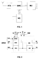
- the base station basically has a block diagram as shown in figure 1. It consists of a radio transceiver RTX in DECT technology, a burst controller BMC, a microcontroller MC and a multiline interface MLI that performs the conversions of analogue to ADPCM coding in the transmit path and from ADPCM to analogue in the receive path. In both processes it carries out an intermediate PCM conversion.
- the radio transceiver RTX includes a transmitter, a receiver and a frequency synthesizer.
- the transmitter serves to transmit, via radio, data bursts coming from the burst controller BMC in the radiofrequency channel determined by the synthesizer.
- the receiver receives, via radio, also in the radiofrequency channel determined by the synthesizer, the bursts proceeding from the terminals with which it is in communication; it also obtains other types of information, such as received field strength, etc.
- the data bursts are located in time slots in accordance with the air interface of the DECT standard, that is, 12 time slots for transmission and an identical number for reception, and 10 possible radiofrequency channels in the band allocated for this type of communication.
- a single radio transceiver is capable of handling a maximum of 12 bidirectional channels although, for this, use can be made of the 10 available frequencies determined by the standard.
- the burst controller BMC has several basic functions. In the first place, it serves to deliver the necessary timing signals so that the data bursts transmitted do so in the defined time slots. In addition, those that are received from the terminals also respect these timing signals, since they are synchronised with the corresponding base station.
- the microcontroller MC serves to control the functions for external interfacing that are used for base station programming, data display, etc.
- the multiline interface MLI serves to set up and control conversations on the side of the interface with the public communications network or with telephone terminals, accordingly.
- the different functions it performs are those of coding/decoding the ADPCM audio channel (voice, fax, etc.), first going through a PCM stage (in which functions of echo cancelling and conference are performed, and suitable time slots are allocated to the line coding devices that work with each audio channel). It also performs the function of ringing current generation and other control functions required for correct operation of the system which are not detailed as they do not form part of the invention.
- the base station has standard, commercially available devices like the PCD 5032 of Philips which, in a simplified form, has a structure as shown in figure 2.
- Each device consists basically of an ADPCM decoder DEC that performs the conversion to PCM of bursts coming from the burst controller BMC, which are the receive side ADPCM signals RAD; an ADPCM coder COD that performs the conversion of PCM information bursts to ADPCM for applying to the burst controller BMC as ADPCM transmit signals TAD; an analogue-to-digital converter A/D which performs the conversion of analogue signals into PCM data, providing an analogue input channel TM in the audio frequency band; and a digital-to-analogue converter D/A that performs the conversion of PCM coded data into analogue output signals RE.
- the output signals, both from the analogue-to-digital converter A/D and from the ADPCM decoder, are joined internally. It also has
- the serial PCM data appear (16 bits), arranged from greater to lesser weighting, at the PCM data output terminal PO, coming from the analogue-to-digital converter A/D which performs the conversion to digital of the audio signal to be transmitted TM.
- the input terminal TPI of the ADPCM coder COD reads the first 14 bits at the same rate as the device clock CLK. While this process lasts, a PCM transmit indication signal TPE takes a low level to indicate this event.
- the serial PCM data appear (16 bits), arranged from greater to lesser weighting, at the PCM data output terminal PO, coming from the ADPCM decoder DEC; simultaneously, the input terminal RPI of the digital-to-analogue converter A/D reads the first 14 bits and performs the conversion to analogue output signals RE; a PCM receive indication signal RPI also takes a low level to indicate this new event.
- the device is in conditions to recommence on the reception of the ADPCM synchronisation pulses RAS.
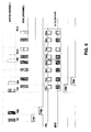
- the interface of the implementation described here and shown in figure 5 can consist of four or six PCD 5032 devices, like the one described, which manage four audio frequency bidirectional channels. Each one of half of them is used to connect a telephone set and the rest serve as outgoing lines into a network of higher order like, for example, the public switched telephone network (though the number of inside and outside lines can be interchanged as long as they add to six).
- the outputs of transmit code presence indication signal TPE and of receive code presence indication signal RPE are joined together to form a single-wire code presence indication bus PE.
- This is also connected to the signal processing means in order to indicate when it will receive new bursts of PCM coded bits via the output PCM bus BPO, and when it has to transmit to the PCM input bus PI, the equivalent burst of the same channel read from the previous frame and after having performed the echo cancelling process.
- the synchronism signal generator SYGEN also carries out a time slot allocation for the channel coding PCD 5032 devices, for which it genetates four synchronisation pulse signals FS1, FS2, FS3 and FS4, whereby each of these is sent, respectively, to one of the devices mentioned. In this way, these pulses determine which time slot is allocated to each device so that they carry out the conversions between the ADPCM-PCM data codings, and vice versa, for both directions of transmission.
- FIG. 6 shows, in the top part, the structure of an ADPCM frame of the audio frequency channels for transmitting (or receiving) formed by 12 equal time slots and with a total duration of 125 ⁇ s.
- the allocation between slots in the ADPCM frame and in the DECT frame at the air interface is flexible and is done under the control of the burst controller itself.
- the synchronisation pulses FS1 and FS2 are also shown in synchronism with slots 1 and 2 of the ADPCM interface and which are applied to the first and second devices. As a consequence of this, the conversion processes in transmission and reception of both are triggered.
- the code presence indication bus PE takes the low level indicating the presence of these data, represented by the pulse TPE1.
- the 16 bits coming from the ADPCM decoder DEC appear on the PCM input bus PI for the receive path and which, similarly, are read by the signal processing means MSP in order to proceed with their treatment.
- the code presence indication bus PE a low level signal appears indicating the presence of these received bits, represented by the pulse RPE1, so that the signal processing means MSP inserts the processed bits of the same received audio frequency channel corresponding to the previous frame in the PCM input bus PI.
- the signals involved are only activated in certain time windows, which permits the insertion of other windows for more effective sharing of the busses employed.
- the second PCD 5032 device receives the second synchronisation pulse FS2, similar to the first but with a delay of 10.4 ⁇ s with respect to it, the 16 bits corresponding to a new audio frequency signal appear on the PCM output bus BPO. This permits the insertion of two audio channels, as can also be seen in figure 6.
- a third synchronisation pulse FS3 which is associated with slot 5 of the ADPCM interface (not with slot 3), the rising edge of which appears 41.23 ⁇ s after the first, is applied to a third PCD 5032 device so that the occupied periods of the PCM output bus BPO, of the code presence indication bus PE, and of the PCM input bus PI do not overlap with the previous ones.
- a fourth synchronisation pulse FS4 is produced in association with slot 6 of the ADPCM interface, the rising edge of which occurs 10.4 ⁇ s after the edge of the third, in such a way that the instants of occupancy of the wires mentioned by a fourth device like those already mentioned, are interleaved with the instants of occupancy of these wires by the third device without any overlapping between them.
- the signal processing means MSP are formed by two signal processors of the type DSP 77C25, each of which permits echo to be cancelled in two channels. One of these processors serves for the cancellation of echo in the first two devices, while the second serves for echo cancelling in the third and fourth devices.
- the fifth and sixth synchronisation pulses should have their rising edge 41.23 ⁇ s after that of the third and fourth pulses respectively, i.e. associated with slots 9 and 10 of the ADPCM interface.
Landscapes
- Engineering & Computer Science (AREA)
- Theoretical Computer Science (AREA)
- Computer Networks & Wireless Communication (AREA)
- Signal Processing (AREA)
- Compression, Expansion, Code Conversion, And Decoders (AREA)
- Transmission Systems Not Characterized By The Medium Used For Transmission (AREA)
- Telephonic Communication Services (AREA)
- Cable Transmission Systems, Equalization Of Radio And Reduction Of Echo (AREA)
- Time-Division Multiplex Systems (AREA)
Applications Claiming Priority (2)
| Application Number | Priority Date | Filing Date | Title |
|---|---|---|---|
| ES9402697 | 1994-12-30 | ||
| ES09402697A ES2103673B1 (es) | 1994-12-30 | 1994-12-30 | Interfaz pcm multilinea para procesado de señal. |
Publications (2)
| Publication Number | Publication Date |
|---|---|
| EP0720401A2 true EP0720401A2 (de) | 1996-07-03 |
| EP0720401A3 EP0720401A3 (de) | 2000-07-12 |
Family
ID=8288457
Family Applications (1)
| Application Number | Title | Priority Date | Filing Date |
|---|---|---|---|
| EP95120270A Withdrawn EP0720401A3 (de) | 1994-12-30 | 1995-12-21 | Vielfachleitung-PCM-Schnittstelle für Signalverarbeitung |
Country Status (5)
| Country | Link |
|---|---|
| US (1) | US5796731A (de) |
| EP (1) | EP0720401A3 (de) |
| JP (1) | JPH08279762A (de) |
| AU (1) | AU706570B2 (de) |
| ES (1) | ES2103673B1 (de) |
Families Citing this family (6)
| Publication number | Priority date | Publication date | Assignee | Title |
|---|---|---|---|---|
| EP0834995A1 (de) * | 1996-10-07 | 1998-04-08 | Alcatel | ADPCM-Transkodierer |
| US6421326B1 (en) * | 1997-07-24 | 2002-07-16 | Innomedia Pte Ltd | Wireless communications system and method |
| AU2388400A (en) | 1999-12-27 | 2001-07-09 | Telogy Networks, Inc. | Digital modem echo canceler enhancement |
| US7551663B1 (en) * | 2001-02-01 | 2009-06-23 | Ipr Licensing, Inc. | Use of correlation combination to achieve channel detection |
| ATE493819T1 (de) * | 2002-03-20 | 2011-01-15 | Igor Borisovich Dounaev | Verfahren und systeme zur digitalen datenübertragung |
| US20040228545A1 (en) * | 2003-05-12 | 2004-11-18 | Kwang-Bo Cho | Multisampling with reduced bit samples |
Family Cites Families (10)
| Publication number | Priority date | Publication date | Assignee | Title |
|---|---|---|---|---|
| DD213339A1 (de) * | 1983-01-25 | 1984-09-05 | Guenther Barthel | Koppelanordnung fuer digitale fernsprechvermittlungszentralen |
| US4777633A (en) * | 1987-08-14 | 1988-10-11 | International Mobile Machines Corp. | Base station for wireless digital telephone system |
| IT1215591B (it) * | 1987-06-26 | 1990-02-14 | Italtel Telematica | Elemento di commutazione di segnali pcm. |
| US5253291A (en) * | 1990-10-18 | 1993-10-12 | Ag Communication Systems Corporation | Hybrid balance and combination codec filter circuit |
| US5247516A (en) * | 1991-03-28 | 1993-09-21 | Sprint International Communications Corp. | Configurable composite data frame |
| KR940004432B1 (ko) * | 1991-10-02 | 1994-05-25 | 삼성전자 주식회사 | 전자교환기의 PCM CODEC(DOCER and DECODER) 집적회로 |
| US5317522A (en) * | 1992-01-15 | 1994-05-31 | Motorola, Inc. | Method and apparatus for noise burst detection in a signal processor |
| US5555287A (en) * | 1992-07-21 | 1996-09-10 | Advanced Micro Devices, Inc. | Integrated circuit and cordless telephone using the integrated circuit |
| FI98429C (fi) * | 1993-08-12 | 1997-06-10 | Nokia Telecommunications Oy | CT2-puhelinjärjestelmä |
| US5600674A (en) * | 1995-03-02 | 1997-02-04 | Motorola Inc. | Method and apparatus of an enhanced digital signal processor |
-
1994
- 1994-12-30 ES ES09402697A patent/ES2103673B1/es not_active Expired - Lifetime
-
1995
- 1995-12-14 AU AU40418/95A patent/AU706570B2/en not_active Ceased
- 1995-12-21 EP EP95120270A patent/EP0720401A3/de not_active Withdrawn
- 1995-12-27 JP JP7341915A patent/JPH08279762A/ja active Pending
- 1995-12-27 US US08/579,406 patent/US5796731A/en not_active Expired - Fee Related
Also Published As
| Publication number | Publication date |
|---|---|
| AU4041895A (en) | 1996-07-11 |
| ES2103673B1 (es) | 1998-05-01 |
| EP0720401A3 (de) | 2000-07-12 |
| US5796731A (en) | 1998-08-18 |
| ES2103673A1 (es) | 1997-09-16 |
| AU706570B2 (en) | 1999-06-17 |
| JPH08279762A (ja) | 1996-10-22 |
Similar Documents
| Publication | Publication Date | Title |
|---|---|---|
| US5237570A (en) | Prioritized data transfer method and apparatus for a radiotelephone peripheral | |
| US5297142A (en) | Data transfer method and apparatus for communication between a peripheral and a master | |
| US4403322A (en) | Voice signal converting device | |
| US6226515B1 (en) | Cellular cordless telecommunications system | |
| US3732374A (en) | Communication system and method | |
| US4740955A (en) | Communications system having voice and digital data capability and employing a plurality of voice and data buses in main service unit and serial packetized transmission to and from telephones | |
| AU604650B2 (en) | Multiplexed digital packet telephone system | |
| US3889063A (en) | Multiplexed digital data communication system | |
| US5420860A (en) | Volume control for digital communication system | |
| US5796731A (en) | Multiline PCM interface for signal processing | |
| US4852157A (en) | Multi-task state machine signalling translator | |
| US4486879A (en) | Method and apparatus for mixing low-frequency signals transmitted via different time slots towards the same telephone receiver set | |
| US5481574A (en) | Synchronization of multiple transmit/receive devices | |
| JPS5972893A (ja) | デイジタル電子切換装置 | |
| US4493949A (en) | Parallel operation of telephone equipment on a digital loop | |
| KR100233469B1 (ko) | 무선사설교환기용 덱트기지국에서 채널데이타 처리시 비트동기화 시스템 | |
| US4601030A (en) | Multipoint system for interconnecting work stations | |
| EP0059543B1 (de) | Parallelbetrieb von Telephongräten auf einer digitalen Teilnehmerleitung | |
| US4800558A (en) | Telephone switching system frame sync generator | |
| JPH04298147A (ja) | 会議通話方式 | |
| JPS59112755A (ja) | 音声交換システム | |
| KR920006142B1 (ko) | 교환기의 인터페이스회로 | |
| EP0596158A1 (de) | Digitaler Fernsprechapparat mit mehreren untereinander verbundenen Schaltungsmodulen | |
| KR900006371Y1 (ko) | 시분할 다중통신 시스템의 슬롯당 디지탈 데이타 입력회로 | |
| JP2654024B2 (ja) | ディジタルボタン電話装置 |
Legal Events
| Date | Code | Title | Description |
|---|---|---|---|
| PUAI | Public reference made under article 153(3) epc to a published international application that has entered the european phase |
Free format text: ORIGINAL CODE: 0009012 |
|
| AK | Designated contracting states |
Kind code of ref document: A2 Designated state(s): DE FR GB IT NL SE |
|
| PUAL | Search report despatched |
Free format text: ORIGINAL CODE: 0009013 |
|
| AK | Designated contracting states |
Kind code of ref document: A3 Designated state(s): DE FR GB IT NL SE |
|
| 17P | Request for examination filed |
Effective date: 20010109 |
|
| GRAH | Despatch of communication of intention to grant a patent |
Free format text: ORIGINAL CODE: EPIDOS IGRA |
|
| STAA | Information on the status of an ep patent application or granted ep patent |
Free format text: STATUS: THE APPLICATION IS DEEMED TO BE WITHDRAWN |
|
| 18D | Application deemed to be withdrawn |
Effective date: 20030614 |