EP0716166B1 - Verfahren zur Herstellung von einkristallinem Material und Verbundmaterial für dieses Verfahren - Google Patents
Verfahren zur Herstellung von einkristallinem Material und Verbundmaterial für dieses Verfahren Download PDFInfo
- Publication number
- EP0716166B1 EP0716166B1 EP95308677A EP95308677A EP0716166B1 EP 0716166 B1 EP0716166 B1 EP 0716166B1 EP 95308677 A EP95308677 A EP 95308677A EP 95308677 A EP95308677 A EP 95308677A EP 0716166 B1 EP0716166 B1 EP 0716166B1
- Authority
- EP
- European Patent Office
- Prior art keywords
- single crystal
- substrate
- layer
- composite material
- crystal material
- Prior art date
- Legal status (The legal status is an assumption and is not a legal conclusion. Google has not performed a legal analysis and makes no representation as to the accuracy of the status listed.)
- Expired - Lifetime
Links
- 239000013078 crystal Substances 0.000 title claims description 54
- 239000002131 composite material Substances 0.000 title claims description 27
- 239000000463 material Substances 0.000 title claims description 18
- 238000004519 manufacturing process Methods 0.000 title claims description 4
- 239000000758 substrate Substances 0.000 claims description 44
- 238000000034 method Methods 0.000 claims description 13
- 239000000126 substance Substances 0.000 claims description 12
- 238000010438 heat treatment Methods 0.000 claims description 8
- 239000000203 mixture Substances 0.000 claims description 6
- QVGXLLKOCUKJST-UHFFFAOYSA-N atomic oxygen Chemical compound [O] QVGXLLKOCUKJST-UHFFFAOYSA-N 0.000 claims description 4
- 229910052760 oxygen Inorganic materials 0.000 claims description 4
- 239000001301 oxygen Substances 0.000 claims description 4
- 238000000137 annealing Methods 0.000 description 13
- 238000001228 spectrum Methods 0.000 description 9
- 229910002370 SrTiO3 Inorganic materials 0.000 description 8
- 238000005001 rutherford backscattering spectroscopy Methods 0.000 description 7
- 230000005465 channeling Effects 0.000 description 5
- 150000002500 ions Chemical class 0.000 description 4
- XUIMIQQOPSSXEZ-UHFFFAOYSA-N Silicon Chemical compound [Si] XUIMIQQOPSSXEZ-UHFFFAOYSA-N 0.000 description 3
- 238000010884 ion-beam technique Methods 0.000 description 3
- 229910052710 silicon Inorganic materials 0.000 description 3
- 239000010703 silicon Substances 0.000 description 3
- 238000000608 laser ablation Methods 0.000 description 2
- GQYHUHYESMUTHG-UHFFFAOYSA-N lithium niobate Chemical compound [Li+].[O-][Nb](=O)=O GQYHUHYESMUTHG-UHFFFAOYSA-N 0.000 description 2
- 238000002360 preparation method Methods 0.000 description 2
- 229910052779 Neodymium Inorganic materials 0.000 description 1
- 229910052784 alkaline earth metal Inorganic materials 0.000 description 1
- 150000001342 alkaline earth metals Chemical class 0.000 description 1
- 229910052782 aluminium Inorganic materials 0.000 description 1
- 229910021417 amorphous silicon Inorganic materials 0.000 description 1
- 230000015572 biosynthetic process Effects 0.000 description 1
- 230000007547 defect Effects 0.000 description 1
- 230000005294 ferromagnetic effect Effects 0.000 description 1
- 238000002513 implantation Methods 0.000 description 1
- 229910052747 lanthanoid Inorganic materials 0.000 description 1
- 150000002602 lanthanoids Chemical class 0.000 description 1
- 229910052746 lanthanum Inorganic materials 0.000 description 1
- 238000005259 measurement Methods 0.000 description 1
- 229910052751 metal Inorganic materials 0.000 description 1
- 239000002184 metal Substances 0.000 description 1
- 229910021645 metal ion Inorganic materials 0.000 description 1
- 229910044991 metal oxide Inorganic materials 0.000 description 1
- 150000004706 metal oxides Chemical class 0.000 description 1
- 229910021421 monocrystalline silicon Inorganic materials 0.000 description 1
- 238000010899 nucleation Methods 0.000 description 1
- 230000006911 nucleation Effects 0.000 description 1
- 150000002926 oxygen Chemical class 0.000 description 1
- 230000000737 periodic effect Effects 0.000 description 1
- 238000005498 polishing Methods 0.000 description 1
- 238000001953 recrystallisation Methods 0.000 description 1
- 239000004065 semiconductor Substances 0.000 description 1
- 238000004544 sputter deposition Methods 0.000 description 1
- 238000003860 storage Methods 0.000 description 1
- 229910052712 strontium Inorganic materials 0.000 description 1
- 239000012808 vapor phase Substances 0.000 description 1
Images


Classifications
-
- C—CHEMISTRY; METALLURGY
- C30—CRYSTAL GROWTH
- C30B—SINGLE-CRYSTAL GROWTH; UNIDIRECTIONAL SOLIDIFICATION OF EUTECTIC MATERIAL OR UNIDIRECTIONAL DEMIXING OF EUTECTOID MATERIAL; REFINING BY ZONE-MELTING OF MATERIAL; PRODUCTION OF A HOMOGENEOUS POLYCRYSTALLINE MATERIAL WITH DEFINED STRUCTURE; SINGLE CRYSTALS OR HOMOGENEOUS POLYCRYSTALLINE MATERIAL WITH DEFINED STRUCTURE; AFTER-TREATMENT OF SINGLE CRYSTALS OR A HOMOGENEOUS POLYCRYSTALLINE MATERIAL WITH DEFINED STRUCTURE; APPARATUS THEREFOR
- C30B1/00—Single-crystal growth directly from the solid state
- C30B1/02—Single-crystal growth directly from the solid state by thermal treatment, e.g. strain annealing
-
- C—CHEMISTRY; METALLURGY
- C30—CRYSTAL GROWTH
- C30B—SINGLE-CRYSTAL GROWTH; UNIDIRECTIONAL SOLIDIFICATION OF EUTECTIC MATERIAL OR UNIDIRECTIONAL DEMIXING OF EUTECTOID MATERIAL; REFINING BY ZONE-MELTING OF MATERIAL; PRODUCTION OF A HOMOGENEOUS POLYCRYSTALLINE MATERIAL WITH DEFINED STRUCTURE; SINGLE CRYSTALS OR HOMOGENEOUS POLYCRYSTALLINE MATERIAL WITH DEFINED STRUCTURE; AFTER-TREATMENT OF SINGLE CRYSTALS OR A HOMOGENEOUS POLYCRYSTALLINE MATERIAL WITH DEFINED STRUCTURE; APPARATUS THEREFOR
- C30B29/00—Single crystals or homogeneous polycrystalline material with defined structure characterised by the material or by their shape
- C30B29/10—Inorganic compounds or compositions
- C30B29/16—Oxides
- C30B29/22—Complex oxides
- C30B29/32—Titanates; Germanates; Molybdates; Tungstates
Definitions
- This invention relates to a process for the preparation of a single crystal material useful as a substrate for forming a superconducting layer, a ferromagnetic layer or a ferroelectric layer thereon.
- the present invention is also directed to a composite material useful for forming such a single crystal material.
- a single crystal substrate generally has surface defects, such as scratches and stains, formed chemically or physically during the manufacture thereof such as in a polishing step or during storage. Thus, it is desirable to recover such damaged surfaces prior to the use thereof.
- a method is adopted in which a silicon single crystal is allowed to epitaxially grow, in a vapor phase, on a surface of a silicon single crystal substrate so that a clean silicon single crystal layer is newly formed thereon.
- This technique cannot be applied to the formation of a metal oxide single crystal such as SrTiO 3 , since it is extremely difficult to control the molar ratio thereof in an oxygen atmosphere.
- US-A-4840816 inter alia discloses a process in which a single crystal of lithium niobate was doped with metal ions by implantation. Under the conditions used the near surface of the lithium niobate was damaged and became essentially amorphous to a depth of about 0.5mm. Subsequently the damaged, implanted single crystal was annealed in a water-saturated oxygen atmosphere which resulted in epitaxial recrystallisation of the damaged region.
- the present invention aims to provide a new process for the preparation of a single crystal material having a clean surface, and also a composite material useful for forming the single crystal material.
- the present invention provides a composite material including a substrate of a single crystal, and a layer of an amorphous substance having the same chemical composition as that of the substrate, the layer having a thickness of 100 ⁇ or less.
- the reference numeral 30 designates a composite material according to the present invention.
- the composite material 30 includes a substrate 10 of a single crystal, and a layer 20 of an amorphous substance having the same chemical composition as that of the substrate 10.
- the substrate 10 is preferably a single crystal having a perovskite structure.
- a perovskite single crystal may be an oxide having the formula ABO 3 wherein A represents an element selected from alkaline earth metals and lanthanoid elements and B represents a metal selected from those belonging to IVB and IIIA of the Periodic Table.
- suitable elements A are Sr, La and Nd, while illustrative of suitable elements B are Ti, Ga and Al.
- the composite material 30 may be produced by forming the amorphous layer 20 over a surface of the substrate 10 by any suitable known method such as by laser ablation or sputtering.
- the amorphous layer 20 of the composite material 30 can be converted and recrystallized into an orderly oriented single crystal layer by a heat treatment (annealing). It is important that the layer 20 should have such a thickness d of 100 ⁇ (lOnm) or less so that the entire layer 20 can epitaxially grow to make a single crystal layer.
- amorphous layer 20 has an excessively large thickness, it becomes impossible for the entire of the layer 20 to epitaxially grow into a single crystal layer.
- the failure of the epitaxial growth is schematically illustrated in Fig. 5, in which designated as 11 is a single crystal substrate and as 12 is an amorphous layer of the same composition as that of the substrate 11.
- amorphous layer 12 on the substrate 11 is subjected to a heat treatment, single crystals 13 epitaxially grow from the interface between the substrate 11 and the amorphous layer 12 toward the opposite surface of the amorphous layer 12.
- the thickness d' of the amorphous layer 12 is excessively large, the nucleation occurs in portions adjacent to the surface of the amorphous layer 12, so that single crystals 14 oriented at random are formed. As a result, there are grown both orderly oriented single crystal layer and randomly oriented single crystal layer on the substrate 11.
- the heat treatment of the composite material 30 is preferably performed at a temperature of up to 1,100°C, more preferably 500-1,100°C in an oxygen atmosphere.
- the annealing may preferably be performed at a temperature of up to 900°C, more preferably 800-900°C and a pressure of 2x10 -6 Torr (2.66x10 -4 Pa) or less.
- a commercially available SrTiO 3 (100) single crystal substrate was subjected to laser ablation at room temperature to form a composite substrate (I) having an amorphous layer with a thickness of 48 ⁇ (4.8 nm) on the substrate. Similar procedure was repeated to obtain composite substrates (II) and (III) having amorphous layers with thickness' of 80 ⁇ (8nm) and 276 ⁇ (27.6 nm), respectively.
- Example 1 Each of the composite substrates (I)-(III) obtained in Example 1 was heated at various temperatures of 500°C, 700°C, 900°C and 1,100°C, for 30 minutes in an oxygen atmosphere of 1 atm (1x10 5 Pa) to obtain single crystal materials.
- Fig. 2 shows the random and [100]-aligned Rutherford backscattering spectra (RBS), wherein the abscissa represents the channel number and the ordinate represents the backscattering yield corresponding to the number of the backscattered ions.
- the spectrum (a) shows the random RBS for the single crystal material obtained by annealing the composite substrate (II)
- the spectrum (b) shows the [100]-aligned RBS for the composite substrate (II)
- the spectrum (c) shows the [100]-aligned RBS for the single crystal material obtained by annealing the composite substrate (II).
- a fragmentary, enlarged view of the spectrum (c) is also shown in Fig. 2 and is indicated by the solid line.
- the spectrum (d) in the dotted line shows the [100]-aligned RBS for the commercially available SrTiO 3 single crystal substrate used in Example 1.
- the backscattering yield of the spectrum (c) is smaller than that of the spectrum (d). It follows that the crystallinity of the single crystal film epitaxially grown on the commercially available single crystal substrate is better than that of the substrate.
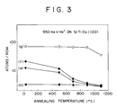
- Fig. 3 shows the annealing temperature dependency of the number of atoms per one row in the channel direction (SPA) measured by the ion channeling using a 950 KeV He + ion beam.
- the plots (e), (f) and (g) are for the single crystal materials obtained by annealing the composite substrates (I), (II) and (III), respectively, while the plot (h) is for the commercially available SrTiO 3 single crystal substrate used in Example 1.
- the annealing temperature is about 900°C or more
- the numbers of atoms in the case of the plots (e) and (f) are similar to or greater than that of the plot (h). It follows that the crystallinity of the single crystal film with a thickness of 48 ⁇ (4.8 nm) or 80 ⁇ (8 nm) epitaxially grown on the commercially available single crystal substrate is comparable to or better than that of the substrate.
- the composite substrate (I) obtained in Example 1 was heated at various temperatures of up to 850°C for 30 minutes under a pressure of 4x10 -7 to 1x10 -6 Torr (5.3x10 -5 to 1.3x10 -4 Pa) to obtain single crystal materials.
- Fig. 4 shows the annealing temperature dependency of the number of atoms per one row in the channel direction measured by the ion channeling using a 950 KeV He + ion beam.
- the plot (i) is for the single crystal material obtained by annealing the composite substrates (I), while the plot (j) is for the commercially available SrTiO 3 single crystal substrate used in Example 1.
- the annealing temperature is about 850°C
- the number of atoms in the case of the plot (i) is similar to that of the plot (j). It follows that the crystallinity of the single crystal film with a thickness of 48 ⁇ (4.8 nm) epitaxially grown on the commercially available single crystal substrate is comparable to that of the substrate.
Landscapes
- Chemical & Material Sciences (AREA)
- Engineering & Computer Science (AREA)
- Crystallography & Structural Chemistry (AREA)
- Materials Engineering (AREA)
- Metallurgy (AREA)
- Organic Chemistry (AREA)
- Physics & Mathematics (AREA)
- Thermal Sciences (AREA)
- Inorganic Chemistry (AREA)
- Crystals, And After-Treatments Of Crystals (AREA)
Claims (6)
- Verfahren zur Herstellung von einkristallinem Material, das die folgenden Schritte umfaßt:Bildung einer Schicht aus einem amorphen Stoff über der Oberfläche eines einkristallinen Substrats, gekennzeichnet dadurch, daß die genannte Schicht eine maximale Dicke von 100 Å (10 nm) aufweist und die chemische Zusammensetzung des amorphen Stoffs der des Substrats entspricht, so daß ein Verbundmaterial entsteht; undErwärmung des Verbundmaterials zwecks Förderung des epitaktischen Wachstums der amorphen Schicht zu einer einkristallinen Schicht.
- Ein Verfahren nach Anspruch 1, gekennzeichnet dadurch, daß es sich bei dem Substrat um ein einzelnes Kristall mit Perowskitstruktur handelt.
- Ein Verfahren nach Anspruch 1 oder 2, gekennzeichnet dadurch, daß die Erwärmung bei einer maximalen Temperatur von 1100 °C in einer Sauerstoffumgebung erfolgt.
- Ein Verfahren nach Anspruch 1 oder 2, gekennzeichnet dadurch, daß die Erwärmung bei einer maximalen Temperatur von 900 °C und einem maximalen Druck von 2 x 10⁻⁶ Torr (2,66 x 10⁻⁴ Pa) erfolgt.
- Ein Verbundmaterial, das aus einem einkristallinen Substrat und einer Schicht eines amorphen Stoffs, dessen chemische Zusammensetzung der des Substrats entspricht, besteht, wobei die genannte Schicht eine maximale Dicke von 100 Å (10 nm) aufweist.
- Ein Verbundmaterial nach Anspruch 5, gekennzeichnet dadurch, daß es sich bei dem Substrat um ein einzelnes Kristall mit Perowskitstruktur handelt.
Applications Claiming Priority (3)
| Application Number | Priority Date | Filing Date | Title |
|---|---|---|---|
| JP30473594 | 1994-12-08 | ||
| JP30473594A JP3244391B2 (ja) | 1994-12-08 | 1994-12-08 | 複合基板及びそれを用いた単結晶基板の製造方法 |
| JP304735/94 | 1994-12-08 |
Publications (2)
| Publication Number | Publication Date |
|---|---|
| EP0716166A1 EP0716166A1 (de) | 1996-06-12 |
| EP0716166B1 true EP0716166B1 (de) | 2000-02-23 |
Family
ID=17936590
Family Applications (1)
| Application Number | Title | Priority Date | Filing Date |
|---|---|---|---|
| EP95308677A Expired - Lifetime EP0716166B1 (de) | 1994-12-08 | 1995-12-01 | Verfahren zur Herstellung von einkristallinem Material und Verbundmaterial für dieses Verfahren |
Country Status (4)
| Country | Link |
|---|---|
| US (1) | US5837053A (de) |
| EP (1) | EP0716166B1 (de) |
| JP (1) | JP3244391B2 (de) |
| DE (1) | DE69515162T2 (de) |
Families Citing this family (8)
| Publication number | Priority date | Publication date | Assignee | Title |
|---|---|---|---|---|
| US5993541A (en) * | 1996-07-31 | 1999-11-30 | Geo Centers Inc | Process for nucleation of ceramics and product thereof |
| US6475725B1 (en) | 1997-06-20 | 2002-11-05 | Baxter Aktiengesellschaft | Recombinant cell clones having increased stability and methods of making and using the same |
| JP3003027B2 (ja) * | 1997-06-25 | 2000-01-24 | 日本ピラー工業株式会社 | 単結晶SiCおよびその製造方法 |
| WO1999000538A1 (en) * | 1997-06-27 | 1999-01-07 | Nippon Pillar Packing Co., Ltd. | SINGLE CRYSTAL SiC AND PROCESS FOR PREPARING THE SAME |
| AT409379B (de) | 1999-06-02 | 2002-07-25 | Baxter Ag | Medium zur protein- und serumfreien kultivierung von zellen |
| JP2003142479A (ja) * | 2001-11-02 | 2003-05-16 | Fujitsu Ltd | 半導体装置、エピタキシャル膜の製造方法、およびレーザアブレーション装置 |
| CA2491992A1 (en) | 2002-07-09 | 2004-01-15 | Baxter International, Inc. | Animal protein free media for cultivation of cells |
| US20060094104A1 (en) | 2004-10-29 | 2006-05-04 | Leopold Grillberger | Animal protein-free media for cultivation of cells |
Family Cites Families (8)
| Publication number | Priority date | Publication date | Assignee | Title |
|---|---|---|---|---|
| US4046618A (en) * | 1972-12-29 | 1977-09-06 | International Business Machines Corporation | Method for preparing large single crystal thin films |
| US4402787A (en) * | 1979-05-31 | 1983-09-06 | Ngk Insulators, Ltd. | Method for producing a single crystal |
| JPS63117985A (ja) * | 1986-11-06 | 1988-05-21 | Matsushita Electric Ind Co Ltd | 酸化物単結晶の製造法 |
| US4840816A (en) * | 1987-03-24 | 1989-06-20 | The United States Of America As Represented By The United States Department Of Energy | Method of fabricating optical waveguides by ion implantation doping |
| JPH0249232A (ja) * | 1988-08-10 | 1990-02-19 | Fujitsu Ltd | 結晶性薄膜の製造方法 |
| FR2667437B1 (fr) * | 1990-09-28 | 1992-10-30 | Commissariat Energie Atomique | Procede de preparation par recuit rapide d'une couche mince en materiau cristallise du type oxyde et substrat revetu d'une couche mince obtenu par ce procede. |
| US5462009A (en) * | 1992-11-06 | 1995-10-31 | The Boeing Company | Method and apparatus for producing perovskite compositions |
| JP3007795B2 (ja) * | 1994-06-16 | 2000-02-07 | シャープ株式会社 | 複合金属酸化物誘電体薄膜の製造方法 |
-
1994
- 1994-12-08 JP JP30473594A patent/JP3244391B2/ja not_active Expired - Fee Related
-
1995
- 1995-11-28 US US08/563,383 patent/US5837053A/en not_active Expired - Fee Related
- 1995-12-01 EP EP95308677A patent/EP0716166B1/de not_active Expired - Lifetime
- 1995-12-01 DE DE69515162T patent/DE69515162T2/de not_active Expired - Fee Related
Also Published As
| Publication number | Publication date |
|---|---|
| EP0716166A1 (de) | 1996-06-12 |
| DE69515162D1 (de) | 2000-03-30 |
| US5837053A (en) | 1998-11-17 |
| JPH08165188A (ja) | 1996-06-25 |
| DE69515162T2 (de) | 2000-06-15 |
| JP3244391B2 (ja) | 2002-01-07 |
Similar Documents
| Publication | Publication Date | Title |
|---|---|---|
| EP1109212B1 (de) | Halbleiteranordnung mit einem kristallinen Erdalkalimetall - Siliziumnitrid/oxid Interface mit Silizium | |
| US6291319B1 (en) | Method for fabricating a semiconductor structure having a stable crystalline interface with silicon | |
| US20010023660A1 (en) | Method for fabricating a semiconductor structure having a crystalline alkaline earth metal oxide interface with silicon | |
| US6248459B1 (en) | Semiconductor structure having a crystalline alkaline earth metal oxide interface with silicon | |
| US6113690A (en) | Method of preparing crystalline alkaline earth metal oxides on a Si substrate | |
| US6528387B1 (en) | SOI substrate and process for preparing the same, and semiconductor device and process for preparing the same | |
| US6224669B1 (en) | Method for fabricating a semiconductor structure having a crystalline alkaline earth metal oxide interface with silicon | |
| US6022410A (en) | Alkaline-earth metal silicides on silicon | |
| EP1069605A2 (de) | Herstellung einer Halbleiterstruktur mit einem Metalloxidinterface zu Silizium | |
| EP1069606A2 (de) | Herstellung einer Halbleiterstruktur mit veringerter Verlusststromdichte | |
| Kijima et al. | New Low-Temperature Processing of Metalorganic Chemical Vapor Deposition-Bi4Ti3O12 Thin Films Using BiO x Buffer Layer | |
| Tiwari et al. | Direct growth of heteroepitaxial CuInSe2 layers on Si substrates | |
| US5837053A (en) | Process for preparing single crystal material and composite material for forming such single crystal material | |
| EP1176230A1 (de) | Verfahren zur Herstellung von kristallinen Erdalkalimetaloxiden auf einem Si-Substrat | |
| Cheng et al. | Ferroelectric properties of (Sr0. 5Ba0. 5) Nb2O6 thin films synthesized by pulsed laser deposition | |
| JPH0354116A (ja) | 複合酸化物超電導薄膜および作製方法 | |
| EP0878847B1 (de) | Nichtflüchtiger Halbleiterspeicher und Verfahren zur Herstellung | |
| Tiwari et al. | Synthesis of epitaxial Pt on (100) Si using TiN buffer layer by pulsed laser deposition | |
| Kalyanaraman et al. | Influence of oxygen background pressure on crystalline quality of SrTiO 3 films grown on MgO by pulsed laser deposition | |
| Shimoyama et al. | Homoepitaxial growth of SrTiO3 in an ultrahigh vacuum with automatic feeding of oxygen from the substrate at temperatures as low as 370° C | |
| CN1217036C (zh) | 在硅衬底上制备结晶碱土金属氧化物的方法 | |
| US7507290B2 (en) | Flux assisted solid phase epitaxy | |
| Tambo et al. | In-situ Annealing of Thin SrO Films Grown on Si (001)-2× 1 by Molecular Beam Epitaxy | |
| JPH09252095A (ja) | 薄膜キャパシタ及び半導体装置 | |
| JP3205666B2 (ja) | Si単結晶基板上でのCeO2 エピタキシャル単結晶薄膜の合成方法 |
Legal Events
| Date | Code | Title | Description |
|---|---|---|---|
| PUAI | Public reference made under article 153(3) epc to a published international application that has entered the european phase |
Free format text: ORIGINAL CODE: 0009012 |
|
| AK | Designated contracting states |
Kind code of ref document: A1 Designated state(s): DE FR GB |
|
| 17P | Request for examination filed |
Effective date: 19961004 |
|
| 17Q | First examination report despatched |
Effective date: 19980909 |
|
| GRAG | Despatch of communication of intention to grant |
Free format text: ORIGINAL CODE: EPIDOS AGRA |
|
| GRAG | Despatch of communication of intention to grant |
Free format text: ORIGINAL CODE: EPIDOS AGRA |
|
| GRAH | Despatch of communication of intention to grant a patent |
Free format text: ORIGINAL CODE: EPIDOS IGRA |
|
| GRAH | Despatch of communication of intention to grant a patent |
Free format text: ORIGINAL CODE: EPIDOS IGRA |
|
| GRAA | (expected) grant |
Free format text: ORIGINAL CODE: 0009210 |
|
| AK | Designated contracting states |
Kind code of ref document: B1 Designated state(s): DE FR GB |
|
| ET | Fr: translation filed | ||
| REF | Corresponds to: |
Ref document number: 69515162 Country of ref document: DE Date of ref document: 20000330 |
|
| PLBE | No opposition filed within time limit |
Free format text: ORIGINAL CODE: 0009261 |
|
| STAA | Information on the status of an ep patent application or granted ep patent |
Free format text: STATUS: NO OPPOSITION FILED WITHIN TIME LIMIT |
|
| 26N | No opposition filed | ||
| REG | Reference to a national code |
Ref country code: GB Ref legal event code: IF02 |
|
| REG | Reference to a national code |
Ref country code: GB Ref legal event code: 732E |
|
| REG | Reference to a national code |
Ref country code: FR Ref legal event code: TQ |
|
| PGFP | Annual fee paid to national office [announced via postgrant information from national office to epo] |
Ref country code: FR Payment date: 20081212 Year of fee payment: 14 |
|
| PGFP | Annual fee paid to national office [announced via postgrant information from national office to epo] |
Ref country code: DE Payment date: 20081127 Year of fee payment: 14 |
|
| PGFP | Annual fee paid to national office [announced via postgrant information from national office to epo] |
Ref country code: GB Payment date: 20081126 Year of fee payment: 14 |
|
| GBPC | Gb: european patent ceased through non-payment of renewal fee |
Effective date: 20091201 |
|
| REG | Reference to a national code |
Ref country code: FR Ref legal event code: ST Effective date: 20100831 |
|
| PG25 | Lapsed in a contracting state [announced via postgrant information from national office to epo] |
Ref country code: FR Free format text: LAPSE BECAUSE OF NON-PAYMENT OF DUE FEES Effective date: 20091231 |
|
| PG25 | Lapsed in a contracting state [announced via postgrant information from national office to epo] |
Ref country code: DE Free format text: LAPSE BECAUSE OF NON-PAYMENT OF DUE FEES Effective date: 20100701 |
|
| PG25 | Lapsed in a contracting state [announced via postgrant information from national office to epo] |
Ref country code: GB Free format text: LAPSE BECAUSE OF NON-PAYMENT OF DUE FEES Effective date: 20091201 |