EP0710051B1 - Schaltungsanordnung und Verfahren zum Betreiben parallel geschalteter Leistungssteller - Google Patents
Schaltungsanordnung und Verfahren zum Betreiben parallel geschalteter Leistungssteller Download PDFInfo
- Publication number
- EP0710051B1 EP0710051B1 EP95116638A EP95116638A EP0710051B1 EP 0710051 B1 EP0710051 B1 EP 0710051B1 EP 95116638 A EP95116638 A EP 95116638A EP 95116638 A EP95116638 A EP 95116638A EP 0710051 B1 EP0710051 B1 EP 0710051B1
- Authority
- EP
- European Patent Office
- Prior art keywords
- current
- power
- circuit
- clock period
- power controller
- Prior art date
- Legal status (The legal status is an assumption and is not a legal conclusion. Google has not performed a legal analysis and makes no representation as to the accuracy of the status listed.)
- Expired - Lifetime
Links
- 238000000034 method Methods 0.000 title claims description 15
- 230000010355 oscillation Effects 0.000 claims description 39
- 230000000630 rising effect Effects 0.000 claims description 16
- 238000004804 winding Methods 0.000 claims description 14
- 230000001960 triggered effect Effects 0.000 claims 1
- 230000004048 modification Effects 0.000 description 4
- 238000012986 modification Methods 0.000 description 4
- 238000009826 distribution Methods 0.000 description 3
- 230000008901 benefit Effects 0.000 description 2
- 230000004913 activation Effects 0.000 description 1
- 230000006978 adaptation Effects 0.000 description 1
- 230000008859 change Effects 0.000 description 1
- 230000001427 coherent effect Effects 0.000 description 1
- 230000003111 delayed effect Effects 0.000 description 1
- 238000010586 diagram Methods 0.000 description 1
- 238000006073 displacement reaction Methods 0.000 description 1
- 230000002349 favourable effect Effects 0.000 description 1
- 238000005286 illumination Methods 0.000 description 1
- 230000000737 periodic effect Effects 0.000 description 1
- 230000008569 process Effects 0.000 description 1
- 230000009467 reduction Effects 0.000 description 1
- 238000004904 shortening Methods 0.000 description 1
Images
Classifications
-
- H—ELECTRICITY
- H02—GENERATION; CONVERSION OR DISTRIBUTION OF ELECTRIC POWER
- H02M—APPARATUS FOR CONVERSION BETWEEN AC AND AC, BETWEEN AC AND DC, OR BETWEEN DC AND DC, AND FOR USE WITH MAINS OR SIMILAR POWER SUPPLY SYSTEMS; CONVERSION OF DC OR AC INPUT POWER INTO SURGE OUTPUT POWER; CONTROL OR REGULATION THEREOF
- H02M5/00—Conversion of ac power input into ac power output, e.g. for change of voltage, for change of frequency, for change of number of phases
- H02M5/02—Conversion of ac power input into ac power output, e.g. for change of voltage, for change of frequency, for change of number of phases without intermediate conversion into dc
- H02M5/04—Conversion of ac power input into ac power output, e.g. for change of voltage, for change of frequency, for change of number of phases without intermediate conversion into dc by static converters
- H02M5/22—Conversion of ac power input into ac power output, e.g. for change of voltage, for change of frequency, for change of number of phases without intermediate conversion into dc by static converters using discharge tubes with control electrode or semiconductor devices with control electrode
- H02M5/25—Conversion of ac power input into ac power output, e.g. for change of voltage, for change of frequency, for change of number of phases without intermediate conversion into dc by static converters using discharge tubes with control electrode or semiconductor devices with control electrode using devices of a thyratron or thyristor type requiring extinguishing means
- H02M5/257—Conversion of ac power input into ac power output, e.g. for change of voltage, for change of frequency, for change of number of phases without intermediate conversion into dc by static converters using discharge tubes with control electrode or semiconductor devices with control electrode using devices of a thyratron or thyristor type requiring extinguishing means using semiconductor devices only
- H02M5/2573—Conversion of ac power input into ac power output, e.g. for change of voltage, for change of frequency, for change of number of phases without intermediate conversion into dc by static converters using discharge tubes with control electrode or semiconductor devices with control electrode using devices of a thyratron or thyristor type requiring extinguishing means using semiconductor devices only with control circuit
- H02M5/2576—Conversion of ac power input into ac power output, e.g. for change of voltage, for change of frequency, for change of number of phases without intermediate conversion into dc by static converters using discharge tubes with control electrode or semiconductor devices with control electrode using devices of a thyratron or thyristor type requiring extinguishing means using semiconductor devices only with control circuit with digital control
Definitions
- the invention relates on the one hand to a method for operating in parallel switched power controller by controlling the power over time several full periods occurring within one cycle period having vibration packages with one rising and one each falling edge and on the other a circuit arrangement to it Execution.
- the Power controllers are periodically (in "clock periods") for delivery driven by power that several during a time slot Full vibrations of a load current, so-called vibration packets, to the connected consumer devices. Often that is from Power controllers to be delivered to the consumer devices Subject to fluctuations and not clear in the case of variable loads determinable in advance.
- the period from the start of the clock period to Start of activation of the relevant power controller (i.e. until Start of the vibration package) is called the delay time.
- the variation of the delay times has no influence on the to the Power delivered by consumer devices because this depends on the Current amplitude and the width of the vibration packets, but not of that Position of the vibration packets within the cycle period.
- the delay time is each Power controller depending on the switch-on time and the Current amplitude of all power controllers set such that within the effective value of the mains current is minimized.
- a such control of the power controller requires the use of a Personnal Computers, whose bus system through the constant adaptation of the Delay times are extremely heavy.
- the invention has for its object a method for operating Power controller connected in parallel with freely changeable power to make available, which largely prevents voltage dips and can be run without the use of a personal computer, and a circuit arrangement for performing the method create.
- the advantage of the method is the reduction in the clock period effective value of the total current drawn from the network (for all consumers connected to the power controller) without this a (highly loaded) bus system of a personal computer is used ought to.
- This effective value corresponds to that formed over a clock period Integral from the square of the total load current, this integral divided by the duration of the clock period (this effective value is i.e. regardless of the duration of a network period).
- the Delay time of the power controller who switched on a current maximum causes a sudden change in the the connected consumer device avoided output.
- a coherent vibration package can be created via the Protruding from one cycle period.
- the location of the clock period the timeline is freely selectable.
- the circuit arrangement for carrying out the method generates one - separate for each power controller - one for the current through the Power controller proportional voltage and on the other hand a Total current of the power controller proportional voltage. These tensions are queried by the microcomputers of the power controllers. Based on these queried values, the Power controller for performing the method according to the invention possible.
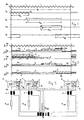
- FIG. 1 shows the profile of the mains voltage U N , which supplies four power controllers connected in parallel.
- a load one or more consumer devices
- the loads are supplied with different power by means of a vibration package control.
- the four power controllers are controlled periodically in such a way that several full periods of the load currents I 1 , I 2 , I 3 and I 4 reach the connected consumer devices.
- Each oscillation packet is represented in FIG. 1 by a rectangle, the height of which corresponds to the effective value of the respective current during the duration of the current flow through the respective power controller.
- the oscillation packets are arranged at different times within the clock period T 0 shown and have different widths.
- FIG. 2 shows again under 2.1 the course of the mains voltage U N within the clock period T 0 and under 2.2 the superposition of the four oscillation packets from FIG. 1.
- This superimposition results in the total load current I N , which is taken from the network to supply all connected loads becomes.
- the oscillation packet which is generated by the current I 4 according to FIG. 1 and has a width of T S4 on the time axis, extends beyond the right edge of the clock period T 0 shown . At the same time, this oscillation packet protrudes from the previous clock period into the clock period T 0 shown .
- This oscillation packet is represented under 2.2 within the clock period T 0 by two areas. One area 4a touches the left edge of the clock period T 0 and the other area 4b touches the right edge.
- these two areas belong to two different, successively occurring vibration packets of the same current I 4 .
- the two areas 4a and 4b can be regarded as a single oscillation packet to explain the method according to the invention. It is worth noting that when the rising edge of area 4b is shifted in the next clock period T 0 , area 4a is also shifted. The two areas 4a and 4b therefore belong together.
- the rising edge of the area 4b of the vibration packet 4 causes a maximum of the total load current in the clock period T 0 , the rising edge of this vibration packet 4b is shifted in the direction of the (temporally) falling edge of another vibration packet, in the case shown to the right in Direction of the falling edge of the oscillation packet 3 or of the oscillation packet 2.
- the area 4a of the oscillation packet 4 shifts to the right (step by step from clock period T 0 to clock period T 0 ), namely until the rising edge of area 4b with the falling edge of (Simultaneously ending) vibration packages 2 and 3 coincide. Then the area 4a has shifted so far to the right that it partially overlaps the vibration packets 1 and 2.
- the position of the clock period T 0 on the time axis is freely selectable, the width of the clock period T 0 is determined by the duration of a period.
- the effective value of the total load current I N below 2.2 is 2.38 A.
- Another example illustrates how the oscillation packet of the power controller, which causes a maximum value of the amplitude of the total current when it is switched on, is shifted to the nearest falling (current) edge (on the time axis) of another oscillation packet.
- This representation shows a different distribution of the vibration packets compared to 2.2 and 2.3, the width and the height of the four vibration packets being identical to those under 2.2 and 2.3, only their position on the time axis is different from the two aforementioned representations.
- a small arrow pointing to the right shows that the rising flank of the oscillation packet 3 is shifted as far as possible to the nearest falling flank of another vibration packet.
- This rising edge causes a maximum value of the total current of all power controllers, ie the first part of the oscillation packet 3, which overlaps the oscillation packet 2, in the clock period T 0 , surpasses all other - partly superimposed - oscillation packets. This fulfills the criterion for the vibration package 3 in which the shifting of the rising edge begins.
- the shifting does not take place in a single step until the next clock period, but the oscillation packet is shifted from clock period T 0 to clock period T 0 by one network period in the desired direction.
- the delay time for the oscillation packet 3 is extended from the clock period T 0 to the clock period T 0 .
- FIG. 2 it can be seen under 2.5 how the oscillation packets are arranged in the clock period T 0 after completion of the displacement of the oscillation pack 3.
- the oscillation packet 3 is not shifted beyond the end of the clock period T 0 , since immediately after this clock period T 0 two rising edges of two overlapping oscillation packets occur, namely of the oscillation packet 1 and the area 4a of the oscillation packet 4. These two oscillation packets 1 and 4 are together higher than the oscillation packet 2.
- a further shift of the oscillation packet 3 to the right would therefore increase the effective value of the total load current in the next clock period T 0 . For this reason, the shift ends with the distribution of the vibration packets 1, 2, 3 and 4 shown in 2.5 (consisting of the areas 4a and 4b).
- the effective value of the total load current (I N ) caused by all four power controllers is only 2.17 A. If the remaining edges of the mains current were equalized (can be represented by a horizontal straight line for the total load current I N ) an effective value of the total load current I N of 2.15 A. At this value, the power output by the four power controllers would produce an actual current I N of constant amplitude. Since the consumer devices in the present example require different power (with different amplitude of the load current), this value cannot be achieved under the conditions given here.
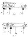
- the thyristor controllers 1 have thyristors 1a, which receive their ignition pulses from a control part 1b assigned to the thyristor controller 1.
- the control parts 1b are equipped with a microcomputer St, which has two inputs 2 and 3 for detecting voltages.
- This second current transformer 5 has its own primary winding for each thyristor controller 1, but only a single secondary winding ⁇ .
- a resistor R B ⁇ is connected to the secondary winding ⁇ and has a voltage proportional to the sum of all the load currents flowing through the thyristor controller 1. This voltage is connected to each microcomputer via electrical connections, namely to input 2.
- the voltage across the resistor R B in the secondary circuit of the first current transformer 4 is conducted - separately for each thyristor controller - to the second input 3 of the associated microcomputer St. In this way, the load current output by the respective thyristor controller 1 is detected.
- the width of the vibration packets and the times of their beginning are controlled via the microcomputers St. With the aid of this circuit arrangement and software stored in the microcomputer, it is therefore possible to carry out the method according to the invention explained in connection with FIG.
- FIG. 4 A modification of the circuit arrangement according to FIG. 3 is shown in FIG. 4.
- This circuit arrangement can only be realized if the mains-side power supply line 6, via which all thyristor controllers 1 are supplied, is accessible.
- a current transformer 7 can be inserted into the current supply line 6, which generates a voltage on the secondary side at a resistor R B ⁇ which is proportional to the total current ⁇ I.
- the voltage across this resistor R B ⁇ is - like the voltage across the resistor R B ⁇ according to FIG. 3 - passed to the input 2 of the microcomputer St.
- the second current transformer 5 according to FIG. 3 is omitted.
- FIG. 5 shows a further modification of the circuit arrangement according to FIG. 3 shown.
- current outputs 8 on the microcomputers St are used to generate a voltage proportional to the total current.
- the current outputs 8 of all microcomputers St are connected to a (common) resistor R B ⁇ .
- the current outputs deliver a current that is proportional to that RMS value of that given by the relevant thyristor controller Load current during the turn-on times of the thyristors 1a.
Description
- der in einer Taktperiode (T0) auftretende Effektivwert des gesamten Laststroms aller Leistungssteller würde bei weiterem Verschieben in dieser Richtung ansteigen oder
- die steigende Flanke des verschobenen Schwingungspakets tritt zum gleichen Zeitpunkt auf wie die fallende Flanke des anderen Schwingungspaketes, und dadurch
- daß in Reihe zu jedem Leistungssteller ein erster Stromwandler mit einem ersten ohmsehen Widerstand im Sekundärkreis liegt, daß jeder Leistungssteller über einem Mikrocomputer angesteuert wird, daß einem dem Gesamtstrom aller Leistungssteller proportionaler Strom über einen zweiten ohmschen Widerstand geleitet wird und daß die an beiden Widerständen anliegenden Spannungen von dem Mikrocomputer abgefragt werden.
- Fig. 1
- Schwingungspakete vierer Leistungssteller,
- Fig. 2
- denkbare Verteillungen der Schwingungspakete innerhalb einer Taktperiode,
- Fig. 3
- eine Schaltungsanordnung mit Summenstromwandler,
- Fig. 4
- eine Abwandlung der Schaltungsanordnung mit einem netzseitigen Stromwandler und
- Fig. 5
- eine Abwandlung der Schaltungsanordnung mit Ausnutzung der Stromausgänge an den Leistungsstellern.
Diese Darstellung zeigt im Vergleich zu 2.2 und 2.3 eine andere Verteilung der Schwingungspakete, wobei die Breite und die Höhe der vier Schwingungspakete mit denen unter 2.2 und 2.3 identisch ist, lediglich ihre Lage auf der Zeitachse ist gegenüber den beiden vorgenannten Darstellungen verschieden.
Diese beiden Schwingungspakete 1 und 4 sind zusammen höher als das Schwingungspaket 2. Eine weitere Verschiebung des Schwingungspaketes 3 nach rechts würde deshalb den Effektivwert des gesamten Laststroms in der nächsten Taktperiode T0 erhöhen. Aus diesem Grunde endet die Verschiebung mit der in 2.5 dargestellten Verteilung der Schwingungspakete 1, 2, 3 und 4 (bestehend aus den Bereichen 4a und 4b). In diesem Fall beträgt der Effektivwert des von allen vier Leistungsstellern verursachten gesamten Laststromes (IN) nur noch 2,17 A. Wenn die noch übrigen Flanken des Netzstromes ausgeglichen wären (darstellbar durch eine waagerechte gerade Linie für den gesamten Laststrom IN), ergäbe sich ein Effektivwert des gesamten Laststroms IN von 2,15 A. Bei diesem Wert würde die von den vier Leistungsstellern abgegebene Leistung einen Lststrome IN konstanter Amplitude hervorrufen. Da die Verbrauchergeräte im vorliegenden Beispiel unterschiedliche Leistung (mit unterschiedlicher Amplitude des Laststroms) benötigen, ist dieser Wert bei den hier gegebenen Verhältnissen nicht erzielbar.
Die Thyristorsteller 1 weisen Thyristoren 1a auf, die ihre Zündimpulse von einem dem Thyristorsteller 1 zugeordneten Steuerteil 1b erhalten. Die steuerteile 1b sind mit einem Mikrocomputer St ausgerüstet, der zwei Eingänge 2 und 3 zur Erfassung von Spannungen aufweist. An jeden Thyristorsteller 1 ist ausgangsseitig ein erster Stromwandler 4 angeschlossen, dessen Primärwicklung in Reihe zum jeweiligen Widerstand RLm (mit m = 1, 2 ...n) liegt. Im Sekundärkreis des ersten Stromwandlers 4 liegt jeweils ein ohmscher Widerstand RB und eine Primärwicklung eines zweiten Stromwandlers 5. Dieser zweite Stromwandlers 5 hat für jeden Thyristorsteller 1 eine eigene Primärwicklung, jedoch nur eine einzige Sekundärwicklung Σ.
An der Sekundärwicklung Σ ist ein Widerstand RBΣ angeschlossen, an dem eine der Summe aller durch die Thyristorsteller 1 fließenden Lastströme proportionale Spannung liegt. Diese Spannung ist über elektrische Verbindungen an jeden Mikrocomputer geführt, und zwar an den Eingang 2.
Mit Hilfe dieser Schaltungsanordnung und einer im Mikrocomputer gespeicherten Software ist es also möglich, das im Zusammenhang mit der Fig.2 erläuterte erfindungsgemäße Verfahren durchzuführen.
Claims (8)
- Verfahren zum Betreiben parallel geschalteter Leistungssteller mittels Steuerung der Leistung über zeitlich innerhalb einer Taktperiode (T0) auftretende, jeweils mehrere Vollperioden aufweisende Schwingungspakete (1, 2, 3, 4) mit jeweils einer steigenden und einer fallenden Flanke,
dadurch gekennzeichnet,
daß die steigende Flanke des Schwingungspaketes (3, 4) desjenigen Leistungsstellers, der bei seinem Einschalten die größte Stromamplitude des gesamten Laststromes (IN) aller Leistungssteller hervorruft, schrittweise von Taktperiode (T0) zu Taktperiode (T0) um jeweils mindestens eine Netzperiode in Richtung der zeitlich nächstliegenden fallenden Flanke eines anderen Schwingungspaketes (2, 3) so lange verschoben wird, bis erstmalig zumindestens eine der beiden folgenden Bedingungen erfüllt ist:der in einer Taktperiode (T0) auftretende Effektivwert des gesamten Laststroms (IN) aller Leistungssteller würde bei weiterem Verschieben in dieser Richtung ansteigen oderdie steigende Flanke des verschobenen Schwingungspakers (3, 4) tritt zum gleichen Zeitpunkt auf wie die fallende Flanke des anderen Schwingungspaketes (2,3). - Verfahren nach Anspruch 1,
dadurch gekennzeichnet,
daß die steigende Flanke schrittweise zeitlich um eine Netzperiode pro Taktperiode (T0) verschoben wird. - Schaltungsanordnung zur Durchführung des Verfahrens nach Anspruch 1 oder 2,
dadurch gekennzeichnet,
daß in Reihe zu jedem Leistungssteller ein erster Stromwandler (4) mit einem ersten ohmschen Widerstand (RB) im Sekundärkreis liegt, daß jeder Leistungssteller über einem Mikrocomputer (St) angesteuert wird, daß einem dem Gesamtstrom aller Leistungssteller proportionaler Strom über einen zweiten ohmschen Widerstand (RBΣ) geleitet wird und daß die an beiden Widerständen (RB, RBΣ) anliegenden Spannungen von dem Mikrocomputer (St) abgefragt werden (Fig. 3). - Schaltungsanordnung nach Anspruch 3,
dadurch gekennzeichnet,
daß der zweite ohmsche Widerstand (RBΣ) im Sekundärkreis eines zweiten Stromwandlers (5, 7) liegt (Fig. 3, Fig. 4). - Schaltungsanordnung nach Anspruch 4,
dadurch gekennzeichnet,
daß der zweite Stromwandler (7) primärseitig vom Gesamtstrom der parallelgeschalteten Leistungssteller durchflossen wird (Fig. 4). - Schaltungsanordnung nach Anspruch 3,
dadurch gekennzeichnet,
daß der zweite Stromwandler (5) für jeden Leistungssteller eine Primärwicklung hat, wobei alle diese Primärwicklungen den gleichen Wicklungssinn haben, daß der durch die Primärwicklungen fließende Strom jeweils mit einem Faktor proportional zu dem durch den jeweiligen Leistungssteller fließenden Strom ist und daß dieser Faktor bei allen Leistungsstellern gleich groß ist (Fig. 3). - Schaltungsanordnung nach Anspruch 6,
darduch gekennzeichnet,
daß die Primärwicklungen des zweiten Stromwandlers (5) in Reihe liegen zu der Sekundärwicklung des jeweiligen ersten Stromwandlers (4) (Fig. 3). - Schaltungsanordnung nach Anspruch 3,
dadurch gekennzeichnet,
daß jeder Leistungssteller während der Dauer der Schwingungspakete über einen Stromausgang (8) einen dem Effektivwert des gerade fließenden Laststromes poportionalen Strom abgibt und daß die Stromausgänge (8) aller Leistungssteller an den zweiten ohmschen Widerstand (RBΣ) angeschlossen sind (Fig.5).
Applications Claiming Priority (2)
| Application Number | Priority Date | Filing Date | Title |
|---|---|---|---|
| DE4437966 | 1994-10-24 | ||
| DE4437966A DE4437966C1 (de) | 1994-10-24 | 1994-10-24 | Verfahren zum Betreiben parallel geschalteter Leistungssteller und Schaltungsanordnung zu seiner Durchführung |
Publications (3)
| Publication Number | Publication Date |
|---|---|
| EP0710051A2 EP0710051A2 (de) | 1996-05-01 |
| EP0710051A3 EP0710051A3 (de) | 1996-09-11 |
| EP0710051B1 true EP0710051B1 (de) | 2000-03-01 |
Family
ID=6531558
Family Applications (1)
| Application Number | Title | Priority Date | Filing Date |
|---|---|---|---|
| EP95116638A Expired - Lifetime EP0710051B1 (de) | 1994-10-24 | 1995-10-23 | Schaltungsanordnung und Verfahren zum Betreiben parallel geschalteter Leistungssteller |
Country Status (2)
| Country | Link |
|---|---|
| EP (1) | EP0710051B1 (de) |
| DE (2) | DE4437966C1 (de) |
Cited By (1)
| Publication number | Priority date | Publication date | Assignee | Title |
|---|---|---|---|---|
| EP2869450A1 (de) | 2013-10-30 | 2015-05-06 | AEG Power Solutions B.V. | Verfahren und Vorrichtung zum Festlegen der Einschaltzeitpunkte von parallel geschalteten Leistungsstellern |
Families Citing this family (7)
| Publication number | Priority date | Publication date | Assignee | Title |
|---|---|---|---|---|
| DE19541869C1 (de) * | 1995-11-09 | 1997-01-16 | Siemens Ag | Verfahren zur Ansteuerung von elektrischen Verbrauchern, insbesondere Heizwiderständen |
| DE19900185A1 (de) * | 1999-01-07 | 2000-07-13 | Ego Elektro Geraetebau Gmbh | Verfahren und Vorrichtung zum Schalten von Verbrauchern eines Elektrogerätes |
| DE10020865A1 (de) * | 2000-04-28 | 2001-11-15 | Aeg Svs Power Supply Systems G | Verfahren zum Betrieb von Leistungsstellern und Schaltungsanordnung zur Durchfuhrung des Verfahrens |
| FR2899038B1 (fr) * | 2006-03-24 | 2008-06-27 | Eurotherm Automation Soc Par A | Procede de determination d'une distribution d'energie a une pluralite de charges electriques et systeme correspondant |
| DE202006014998U1 (de) * | 2006-09-28 | 2007-01-11 | Aeg Power Supply Systems Gmbh | Dreiphasige Schaltungsanordnung |
| EP2187516B1 (de) | 2008-11-14 | 2014-11-05 | AEG Power Solutions GmbH | Schaltungsanordnung parallel geschalteter Leistungssteller zur gleichmäßigen Verteilung der Leistungsaufnahme aus dem Wechselspannungsnetz |
| GB0910141D0 (en) | 2009-06-12 | 2009-07-29 | Eurotherm B V | Improvements in the distribution and utilisation of electrical energy in industrial processes |
Family Cites Families (2)
| Publication number | Priority date | Publication date | Assignee | Title |
|---|---|---|---|---|
| DE3539581A1 (de) * | 1985-11-08 | 1987-05-21 | Philips Patentverwaltung | Verfahren zum steuern mehrerer elektrischer lasten |
| DE4309031A1 (de) * | 1992-03-30 | 1993-10-21 | Licentia Gmbh | Verfahren zum Betreiben mehrerer parallel geschalteter Thyristorsteller |
-
1994
- 1994-10-24 DE DE4437966A patent/DE4437966C1/de not_active Expired - Fee Related
-
1995
- 1995-10-23 DE DE59507892T patent/DE59507892D1/de not_active Expired - Lifetime
- 1995-10-23 EP EP95116638A patent/EP0710051B1/de not_active Expired - Lifetime
Cited By (1)
| Publication number | Priority date | Publication date | Assignee | Title |
|---|---|---|---|---|
| EP2869450A1 (de) | 2013-10-30 | 2015-05-06 | AEG Power Solutions B.V. | Verfahren und Vorrichtung zum Festlegen der Einschaltzeitpunkte von parallel geschalteten Leistungsstellern |
Also Published As
| Publication number | Publication date |
|---|---|
| DE59507892D1 (de) | 2000-04-06 |
| EP0710051A3 (de) | 1996-09-11 |
| DE4437966C1 (de) | 1995-11-02 |
| EP0710051A2 (de) | 1996-05-01 |
Similar Documents
| Publication | Publication Date | Title |
|---|---|---|
| DE19545154C2 (de) | Stromversorgungseinrichtung | |
| EP0225657B1 (de) | Verfahren zum Steuern mehrerer elektrischer Lasten | |
| EP0491731B1 (de) | Schaltnetzteil | |
| EP0283842B1 (de) | Umrichterschaltung mit einem Eintakt-Sperrumrichter | |
| DE19539976A1 (de) | Treiberschaltung hohen Wirkungsgrades für ein magnetisches Lagersystem | |
| EP0710051B1 (de) | Schaltungsanordnung und Verfahren zum Betreiben parallel geschalteter Leistungssteller | |
| DE19545360B4 (de) | Gleichstromleistungsquelle | |
| EP0685940B1 (de) | Pulsweitenmodulierter Schaltwandler zum Betrieb elektrischer Verbraucher | |
| EP0708998B1 (de) | Gepuffertes gleichspannungsversorgungssystem | |
| DE2022621C3 (de) | Steuerschaltung für einen statischen Wechselrichter | |
| EP1380097A2 (de) | Weshselrichter | |
| EP0620635B1 (de) | Gesteuerter Drehstrom-Gleichrichter | |
| EP0872941B1 (de) | Verfahren zur zentralen Blindleistungskompensation in einem ein- oder mehrphasigen Wechselstromnetz und Vorrichtung zur Durchführung desselben | |
| DE2838062C2 (de) | Anordnung mit parallelgeschalteten Gleichstrom-Umrichtern | |
| DE19942203B4 (de) | Verfahren zur Ausgangsspannungsbegrenzung für einen spannungs-/frequenzgeführten Umrichter | |
| EP1105964B1 (de) | Schaltungsanordnung zum regeln der drehzahl eines lüfters | |
| DE2554743A1 (de) | Treiberschaltung fuer wechselnde induktive last | |
| EP1533886B1 (de) | Verfahren zum Betreiben eines Hochsetzstellers | |
| DE3816536A1 (de) | Verfahren und einrichtung zur regelung eines gleichstromes mit hilfe von parallel geschalteten gleichstromstellern | |
| DE10160790A1 (de) | Schaltungsanordnung zum Einschalten einer Teilschaltungsanordnung | |
| DE3444035C2 (de) | ||
| EP0484570B1 (de) | Sperrwandler-Schaltnetzteil | |
| DE1463763C3 (de) | Dreiphasige Wechselspannungsregelanordnung | |
| DE2007694B2 (de) | Spannungsregelgerät mit schaltendem Stellglied | |
| DE3631932A1 (de) | Spannungswandler |
Legal Events
| Date | Code | Title | Description |
|---|---|---|---|
| PUAI | Public reference made under article 153(3) epc to a published international application that has entered the european phase |
Free format text: ORIGINAL CODE: 0009012 |
|
| AK | Designated contracting states |
Kind code of ref document: A2 Designated state(s): DE FR GB IT |
|
| PUAL | Search report despatched |
Free format text: ORIGINAL CODE: 0009013 |
|
| RAP1 | Party data changed (applicant data changed or rights of an application transferred) |
Owner name: AEG STROMVERSORGUNGS-SYSTEME GMBH |
|
| AK | Designated contracting states |
Kind code of ref document: A3 Designated state(s): DE FR GB IT |
|
| 17P | Request for examination filed |
Effective date: 19960828 |
|
| RAP1 | Party data changed (applicant data changed or rights of an application transferred) |
Owner name: AEG SVS POWER SUPPLY SYSTEMS GMBH |
|
| GRAG | Despatch of communication of intention to grant |
Free format text: ORIGINAL CODE: EPIDOS AGRA |
|
| GRAG | Despatch of communication of intention to grant |
Free format text: ORIGINAL CODE: EPIDOS AGRA |
|
| GRAH | Despatch of communication of intention to grant a patent |
Free format text: ORIGINAL CODE: EPIDOS IGRA |
|
| 17Q | First examination report despatched |
Effective date: 19990805 |
|
| GRAH | Despatch of communication of intention to grant a patent |
Free format text: ORIGINAL CODE: EPIDOS IGRA |
|
| GRAA | (expected) grant |
Free format text: ORIGINAL CODE: 0009210 |
|
| AK | Designated contracting states |
Kind code of ref document: B1 Designated state(s): DE FR GB IT |
|
| PG25 | Lapsed in a contracting state [announced via postgrant information from national office to epo] |
Ref country code: IT Free format text: LAPSE BECAUSE OF FAILURE TO SUBMIT A TRANSLATION OF THE DESCRIPTION OR TO PAY THE FEE WITHIN THE PRE;WARNING: LAPSES OF ITALIAN PATENTS WITH EFFECTIVE DATE BEFORE 2007 MAY HAVE OCCURRED AT ANY TIME BEFORE 2007. THE CORRECT EFFECTIVE DATE MAY BE DIFFERENT FROM THE ONE RECORDED.SCRIBED TIME-LIMIT Effective date: 20000301 |
|
| REF | Corresponds to: |
Ref document number: 59507892 Country of ref document: DE Date of ref document: 20000406 |
|
| GBT | Gb: translation of ep patent filed (gb section 77(6)(a)/1977) |
Effective date: 20000530 |
|
| ET | Fr: translation filed | ||
| PLBE | No opposition filed within time limit |
Free format text: ORIGINAL CODE: 0009261 |
|
| STAA | Information on the status of an ep patent application or granted ep patent |
Free format text: STATUS: NO OPPOSITION FILED WITHIN TIME LIMIT |
|
| 26N | No opposition filed | ||
| REG | Reference to a national code |
Ref country code: GB Ref legal event code: IF02 |
|
| PGFP | Annual fee paid to national office [announced via postgrant information from national office to epo] |
Ref country code: DE Payment date: 20141031 Year of fee payment: 20 Ref country code: FR Payment date: 20141022 Year of fee payment: 20 Ref country code: GB Payment date: 20141021 Year of fee payment: 20 |
|
| REG | Reference to a national code |
Ref country code: DE Ref legal event code: R082 Ref document number: 59507892 Country of ref document: DE Representative=s name: FRITZ PATENT- UND RECHTSANWAELTE PARTNERSCHAFT, DE |
|
| REG | Reference to a national code |
Ref country code: DE Ref legal event code: R082 Ref document number: 59507892 Country of ref document: DE Representative=s name: FRITZ PATENT- UND RECHTSANWAELTE PARTNERSCHAFT, DE Effective date: 20150325 Ref country code: DE Ref legal event code: R081 Ref document number: 59507892 Country of ref document: DE Owner name: ADVANCED ENERGY INDUSTRIES GMBH, DE Free format text: FORMER OWNER: AEG SVS POWER SUPPLY SYSTEMS GMBH, 59581 WARSTEIN, DE Effective date: 20150325 |
|
| REG | Reference to a national code |
Ref country code: GB Ref legal event code: 732E Free format text: REGISTERED BETWEEN 20150514 AND 20150520 |
|
| REG | Reference to a national code |
Ref country code: FR Ref legal event code: CD Owner name: AEG POWER SOLUTIONS GMBH Effective date: 20150710 |
|
| REG | Reference to a national code |
Ref country code: DE Ref legal event code: R071 Ref document number: 59507892 Country of ref document: DE |
|
| REG | Reference to a national code |
Ref country code: GB Ref legal event code: PE20 Expiry date: 20151022 |
|
| REG | Reference to a national code |
Ref country code: FR Ref legal event code: TP Owner name: ADVANCED ENERGY INDUSTRIES GMBH, DE Effective date: 20151110 |
|
| PG25 | Lapsed in a contracting state [announced via postgrant information from national office to epo] |
Ref country code: GB Free format text: LAPSE BECAUSE OF EXPIRATION OF PROTECTION Effective date: 20151022 |