EP0708492B1 - Microstrip patch antenna and its particular application in a timepiece - Google Patents
Microstrip patch antenna and its particular application in a timepiece Download PDFInfo
- Publication number
- EP0708492B1 EP0708492B1 EP95116148A EP95116148A EP0708492B1 EP 0708492 B1 EP0708492 B1 EP 0708492B1 EP 95116148 A EP95116148 A EP 95116148A EP 95116148 A EP95116148 A EP 95116148A EP 0708492 B1 EP0708492 B1 EP 0708492B1
- Authority
- EP
- European Patent Office
- Prior art keywords
- conductive element
- antenna
- frequency adjustment
- center
- adjustment plate
- Prior art date
- Legal status (The legal status is an assumption and is not a legal conclusion. Google has not performed a legal analysis and makes no representation as to the accuracy of the status listed.)
- Expired - Lifetime
Links
Images


Classifications
-
- H—ELECTRICITY
- H01—ELECTRIC ELEMENTS
- H01Q—ANTENNAS, i.e. RADIO AERIALS
- H01Q1/00—Details of, or arrangements associated with, antennas
- H01Q1/27—Adaptation for use in or on movable bodies
- H01Q1/273—Adaptation for carrying or wearing by persons or animals
-
- H—ELECTRICITY
- H01—ELECTRIC ELEMENTS
- H01Q—ANTENNAS, i.e. RADIO AERIALS
- H01Q9/00—Electrically-short antennas having dimensions not more than twice the operating wavelength and consisting of conductive active radiating elements
- H01Q9/04—Resonant antennas
- H01Q9/0407—Substantially flat resonant element parallel to ground plane, e.g. patch antenna
Definitions
- the present invention relates to antennas intended for convert an alternating voltage into a microwave and vice versa and, more particularly, to antennas of this type comprising a separate conductive element and a ground plane by a dielectric substrate. These antennas are also known under the English name "microstrip patch antennas".
- the invention can be used to transmit and / or receive GPS signals ("Global Positioning System"), and, moreover, it can be incorporated into watches or other products watchmakers. The invention will therefore be described in the context of this application example. However, it will be understood that the invention is of course not limited to this application.
- the miniaturization of the antennas of the type described above is usually accomplished by using a substrate of a very high permittivity. This invariably involves the use of a ceramic substrate. The costs of manufacture of such a substrate are often high.
- a miniaturized antenna is known from the patent application EP-A-0 525 726.
- This document describes a polarized antenna circular comprising a dielectric substrate having two opposite sides. On one side is fixed a ground plane and on the other side is fixed a conductive element.
- This element conductor is provided with an electrical excitation point off-center with respect to the axis of rotation of the antenna. It is also provided with slots placed at its periphery and passing virtually through its center. The characteristics of these slots, such as their length or positioning at the periphery of the conductive element, used to determine the resonant frequency of the antenna.
- Another antenna of this type is also known from the publication IEEE Transactions on vehicular technology, vol.40, no.2, May 1991, New York US pages 483-486, entitled "A flat energy density antenna system for mobile telephone ”.
- This publication also describes the use of slots allowing in particular to increase the resonant frequency of the antenna by reducing the effective radius of the element conductor, i.e. by reducing the length of the slots used.
- Miniature antennas of this type have a width very narrow band. Therefore, under tolerances manufacturing, design and construction of these antennas is a difficult task.
- the mechanical adjustment of edges of the conductive element is a technique used long time to get the resonant frequency of the desired antenna.
- such a solution is both destructive and cumbersome.
- the object of the present invention is to provide an antenna miniaturized of the type defined above which remedies everything less in part to the disadvantages of state antennas prior art.
- Another object of the invention is to provide an antenna miniaturized of the type defined above which is compact, and which is relatively easy and inexpensive to manufacture.
- an object of the invention is to provide a miniaturized antenna of the type defined above which allows a simple adjustment of its resonant frequency.
- Another object of the invention is to provide an antenna miniaturized of the type defined above which is capable of being used in a watch.
- the invention therefore relates to an antenna intended to convert an alternating voltage, coming from a antenna circuit, in a wave with linear polarization and vice versa, the characteristics of which are set out in claim 1.
- the invention also relates to an antenna intended for convert alternating voltage from a circuit antenna, in a wave with linear or circular polarization and vice versa, the characteristics of which are set out in claim 8.
- the invention allows the creation of a miniaturized antenna without requiring the use of a very high permittivity substrate.
- the antenna comprises an adjustment plate frequency, mounted on the center of the conductive element and on an axis perpendicular to the plane of the conductive element, the distance between the periphery and the center of the plate, the along the axis where the slots extend, being variable by so that, by rotation, the adjustment plate frequency acts to modify the effective length of the slots.
- the rotation of the plate frequency adjustment around its axis allows, an adjustment simple and precise antenna resonant frequency, and this over a bandwidth greater than the width of conductive element strip.
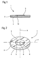
- the arrangement of the miniaturized antenna 1 according to the invention shown in Figures 1 and 2 includes a dielectric substrate 2, a conductive element 3 and a ground plane 4.
- the conductive element 3 has the form general of a disc and according to the Anglo-Saxon denomination is called "radiating patch".
- the conductive element 3 and the ground plane 4 are deposited on surfaces opposite of the dielectric substrate 2.
- the antenna 1 has a geometry suitable for receiving and emitting waves at linear polarization.
- the conductive element 3 has slots 5 and 6 diametrically opposite and aligned along the axis 7. These slots 5 and 6 extend from the periphery towards the center of the conductive element 3.
- An excitation point 8 is located in the plane of the conductive element 3, on a axis 9 which is perpendicular to axis 7. The excitation is ensured by means of a coaxial cable whose conductor central 10 passes through the substrate 2 and is welded to the element conductor 3 at the point of excitation 8.
- FIG. 3 shows more precisely the geometry of the conductive element 3. It can be seen that the slots 5 and 6 both have a length r x and that the conductive element 3 has a diameter 2R, R being the radius of the latter.
- the slots 5 and 6 constitute a capacitive load for the antenna 1.
- Theoretical considerations which will not be repeated here since they go beyond the scope of the present patent application, show that the resonance frequency of the antenna 1 strongly depends of the length r x of the slots 5 and 6. According to these considerations, when r x is zero, the antenna 1 resonates at a frequency f c . However, when the value of r x approaches R, the resonant frequency approaches f c / 2.
- the diameter 2R of the antenna is a function of the inverse of the resonance frequency f c thereof.
- the resonance frequency f c is close to f c / 2 for a certain dimension 2R, one can also choose to reduce the dimension 2R by half for a certain resonance frequency f c . That is to say, the maximum dimension of the antenna 1 can be reduced by a factor of 2 when the slots extend substantially over the entire distance separating the periphery from the center of said conductive element.
- the slots 5 and 6 can be produced by cutting the conductive element 3 by means of a laser beam. Of course, the slots 5 and 6 can also be produced by etching or any other chemical or mechanical treatment of the conductive element 3.
- the circular shape of the element conductor 3 of figures 2 and 3 represents only one example of a form of the conductive element of the invention.
- a square shape can also be used, as well as any other conductive element which is delimited at its periphery by an edge which gives this element a double planar symmetry along two axes perpendicular.
- the excitation point is on one of the two axes of symmetry of the conductive element and the slots 5 and 6 extend on the other axis of symmetry.
- Figure 4 shows the geometry of an element conductor 20 capable of receiving and transmitting both circularly polarized signals as signals to linear polarization.
- the conductive element 20 comprises slots 21 and 22 which extend from its periphery towards the center and which are aligned on the same axis 23.
- the conductive element 20 includes slots 24 and 25 which extend from its periphery towards the center and which are aligned on the same axis 26 perpendicular to the axis 23.
- An excitation point 27 is located on an axis 45 ° offset from the two axes 23 and 24.
- the lengths r x of the slots 21 and 22 and r y of the slots 24 and 25 must be equal.
- a right circular polarization is obtained if, for an excitation point 27 as described above, r x is greater than r y according to a suitable choice.
- the circular shape of the conductive element 20 of FIG. 4 only represents a particular shape of the conductive element of the invention. It goes without saying that a square shape can also be used or any other form of conductive element delimited at its periphery by an edge which gives it a double planar symmetry along two perpendicular axes.
- the excitation point 27 of the conductive element is on a bisecting axis of the angle formed between the two axes of symmetry.
- the pairs of slots 21, 22 and 23, 24 extend respectively on the two axes of symmetry.
- the resonant frequency of the antenna according to the invention varies as a function of the distance r, if we consider the conductive element 3 of FIG. 3, or as a function of the distances r x and r y , if we consider the conductive element shown in FIG. 4.
- r the distance between the conductive elements 3 of FIG. 3
- r x and r y the distance between the conductive elements shown in FIG. 4.
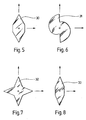
- Figures 5, 6, 7 and 8 show respectively examples 30, 31, 32 and 33 of geometries of such a plate frequency adjustment, the distance between the periphery and the center of said plate, along at least one of axes defined by the slots of the conductive element, varying according to the angle of rotation of the plate about an axis perpendicular A to the plane of the plate and passing through the center of the plate relative to the element driver.
- the structures shown in Figures 5 to 8 can be done in several ways. For example, they can be printed on a dielectric substrate or machined from a metal block. Several forms of plates are possible and the choice of these depends on the necessary tuning range as well as the finesse of the agreement.
- Figures 9 and 10 show an antenna 40 comprising a dielectric substrate 41, a ground plane 42, a conductive element 43 and an adjustment plate frequency 44, the latter being separated from the element conductor 43 by another dielectric substrate 45.
- the conductive element 43 has orthogonal slots 46, 47, 48 and 49.
- the rotation of the adjustment plate frequency 44 around axis A with respect to the element conductor 43 changes the effective lengths of the slots 46 to 49 and, therefore, changes the frequency of antenna resonance 40.
- the antenna 40 also comprises a coaxial connector whose central conductor 50 passes through the substrate 41.
- the central conductor. 50 is welded to the element conductor 43, while the outer conductor is soldered to ground plane 42.
- the two conductors of the connector coaxial are also connected to an antenna circuit.
- the antenna 40 converts an alternating voltage from of the antenna circuit, between the two conductors of the coaxial connector, into a microwave and vice versa.
- the antenna 40 has a central support 51 which passes through openings 52, 53 and 54 in the center of the structure shown in Figure 9 and which maintains the alignment of the various elements of the antenna 40.
- the central support 51 can be realized either in material insulating or conductive material, the difference related to the use of one or the other of these two materials being a small change in the resonant frequency. This difference can be offset anyway by a rotation of the frequency adjustment plate 44.
- the center of the conductive element 43 is a point of zero tension and that the fact that this point either in open circuit or in short circuit with ground does not affect the characteristics of the antenna.
- the conductive element 20 is linearly polarized along a line passing through the center of the conductive element 20 and by the excitation point 27.
- this linear polarization can be adjusted.
- adjusting the resonant frequency of an antenna is only required for overcome the uncertainty of the value of the permittivity of the substrate.
- the antenna can be adjusted by using the disturbance segments that come to be described.
- Frequency adjustment plates simple narrow band can be used so that the antenna can be tuned to a desired frequency.
- Figures 13, 14 and 15 show examples of shape plates 70, 71 and 72.
- Figure 16 shows the arrangement of the frequency adjustment plate 70 of FIG. 13 and of the conductive element 65 of FIG. 12.
- FIG. 17 shows the arrangement of the frequency adjustment plate 72 of FIG. 15 and of the conductive element 64 of the figure 11. Note that the shape and size of the frequency adjustment plates 70, 71 and 72 relative to to the corresponding conductive elements are such that the distance between the periphery and the center of the plates 70, 71 and 72 vary little depending on the angle of rotation.
- FIGS. 7 and 8 show an example of such a combination of plates.
- the frequency adjustment plates 32 and 33 are supported above the conductive element 20 of FIG. 4.
- the adjustment plate can first be rotated 32 to establish linear polarization at a desired frequency.
- the frequency adjustment plate 33 can be rotated to introduce a controlled offset between the dimensions r x and r y , which leads the antenna to circular polarization operation.
- the use of two frequency adjustment plates makes it possible to be able to provide wider manufacturing tolerances for the antenna.
- a conductive element having the shape shown in FIG. 3 is etched from a substrate made of a material sold under the trade designation ULTRALAM®.
- the initial dimensions of the substrate were 144 x 1.5 mm 3 and its relative permittivity is 2.5.
- a circular hole with a diameter of 1 mm is drilled in the center of the substrate.
- the antenna is energized by means of a signal applied to the conductive element 3 via a standard 50 ⁇ SMA coaxial cable.
- a hole with a diameter equal to 3 ⁇ is formed in the center of the conductive element.
- a frequency adjustment plate was used having the shape shown in Figure 5.
- the arrangement of the antenna is represented in figure 19.
- the plate of frequency setting is burned from a disc circular in epoxy. We chose this material in this case due to its great rigidity.
- the circular disc has a thickness of 0.8 mm and a diameter of 60 mm.
- another epoxy disc such as that referenced 45 in Figure 9. This disc serves as a plate spacing between the conductive element and the plate frequency setting.
- the spacer plate has a thickness of 0.1 mm and a diameter of 25 mm.
- the angle of rotation of the plate frequency adjustment 33 of the antenna shown in the figure 19 is limited to a value of 90 °.
- the use of the frequency adjustment plate shown in Figure 6 allows rotation by an angle 180 ° and therefore a finer adjustment of the frequency in the same frequency range.
- An antenna was made having an arrangement such as that shown in FIG. 18. This antenna was excited at a single point situated on an axis bisecting the angle formed between the two orthogonal axes of the slots of the conductive element.
- this excitation technique is quite sensitive compared to other known techniques and that it requires a precise separation between the two degenerate modes of the antenna.
- the geometry of the conductive element shown in Figure 4 can be adapted for this purpose using an asymmetrical frequency adjustment structure.
- a circularly polarized excitation requires asymmetry in the dimensions of the slots of the conductive element.
- the fact that the length r x is greater than the length r y leads to circular polarization to the right.
- the conductive element is etched from a substrate made of a material sold under the trade designation ULTRALAM®.
- the initial dimensions of the substrate were 144 x 144 x 1.5 mm 3 and its relative permittivity is 2.5.
- a circular hole with a diameter of 1 mm is drilled in the center of the substrate.
- the antenna is energized by means of a signal applied to the conductive element 3 via a standard 50 ⁇ SMA coaxial cable.
- a hole with a diameter equal to 3 ⁇ is provided in the center of the conductive element.
- Frequency adjusting plates having the form shown in Figures 7 and 8 are used.
- the antenna layout is shown in Figure 18.
- the frequency adjustment plate of figure 7 is engraved from a circular epoxy disc.
- the disc circular has a thickness of 0.1 mm and a diameter of 60 mm.
- the frequency adjustment plate of figure 8 is also engraved from a circular disc in epoxy.
- the circular disc has a thickness of 0.8 mm and a diameter of 50 mm.
- Another epoxy disc like that designated by the reference numeral 45 in FIG. 9, is used as a spacer plate and is arranged between the conductive element and the frequency adjustment plate.
- the spacer plate has a thickness of 0.1 mm and a 25 mm diameter. No spacer disc is used between the two frequency adjustment plates.
- the range of adjustment of the resonant frequency of the antenna is slightly lower than the adjustment range from the previous example due to the lag between two degenerate modes of the antenna in the second example. This variation is around 10%.
- the report standing waves in tension, measured at resonance, is better than 2 at a frequency of 2.306 MHz.
- a conductive element having the shape shown in FIG. 11 is etched from a substrate made of a material sold under the trade name TMM-10®, this conductive element comprising disturbance segments allowing operation with circular polarization to the right.
- the substrate is circular and has a diameter of 34.5 mm.
- the thickness of the substrate is 0.635 mm and its relative permittivity is 9.2.
- a circular hole with a diameter of 1.4 mm is drilled in the center of the substrate.
- the antenna is energized by means of a signal applied to the conductive element via a standard 50 ⁇ SMA coaxial cable.
- a frequency adjustment plate was used having the shape shown in Figure 15.
- the arrangement of the antenna is represented in figure 17.
- the plate of frequency setting is burned from a disc circular in epoxy. This material is preferred here in because of its great rigidity.
- the circular disc has a 0.8 mm thick and 25 mm in diameter.
- a disk TEFLON® dielectric is used as a plate and is arranged between the conductive element and the frequency adjustment plate.
- the spacer plate has a thickness of 0.254 mm and a diameter of 25 mm. This structure provides a range of adjustment frequency of the order of 2%.
- the antenna is adjusted to the frequency of GPS signals (1.57542 GHz) by the rotation of the adjustment plate frequency.
- the measured axial ratio is 2.54 dB and the bandwidth, with a standing wave ratio in voltage equal to 2, is 12 MHz.
- the gain measured is -6 dBi.
- Example 4 Circular polarization and band adjustment narrow.
- This example uses a conductive element comprising disturbance segments for operation with right-hand circular polarization.
- a conductive element having the shape shown in FIG. 12 is etched from a TMM-10® substrate.
- the substrate is circular and has a diameter of 34.5 mm.
- the thickness of the substrate is 1.27 mm and its relative permittivity is 9.2.
- a circular hole with a diameter of 1.4 mm is drilled in the center of the substrate.
- the antenna is energized by means of a signal applied to the conductive element via a standard 50 ⁇ SMA coaxial cable.
- a hole with a diameter equal to 1.631 mm is drilled in the center of the conductive element.
- a frequency adjustment plate having the form shown in figure 13 is machined from a block of copper. No spacer disc is used, but an air gap is created by supporting the adjustment plate frequency 0.2 mm above the conductive element at by means of a central support element.
- the layout of the antenna is illustrated in Figure 16.
- the plate geometry frequency setting 70 is such that the distance between its periphery and its origin varies linearly between 4.5 mm and 8.75 mm depending on the angle of rotation thereof.
- the antenna in this example is mounted in a housing plastic and is set to the frequency of GPS signals (1.57542 GHz) by rotation of the adjustment plate frequency.
- the measured axial ratio, with the housing fixed at the antenna ground plane, is 1.78 dB and the bandwidth when the standing wave ratio in voltage is equal to 2 is 11 MHz.
- the gain measured is -4.0 dB.
- the frequency adjustment plate 70 can be replaced by the frequency adjustment plate 71 of FIG. 14.
- This frequency adjustment plate is easier to manufacture because it can be made from bars currently available in the trade.
- the adjustment range in this case is around 3% and the maximum angle of rotation is 45 °.
- the geometry of the element conductor allows proper size control. of the current shapes such as circular shapes or rectangular have a fixed size according to the frequency of desired resonance and according to the characteristics of the substrate used. Using a slot length variable, you can modify the antenna dimensions by a factor of 2. Furthermore, the shape of the conductive element allows optimal use of the available space, because there is little unmetallized surface. Consequently, the invention allows miniaturization of the antenna while keeping an optimal gain / size ratio.
- Examples 3 and 4 above describe antennas which are intended to receive, waves of GPS signals transmitted by satellite.
- the dimensions of the antenna are as it can be mounted in a watch case.
- the antenna can for example be arranged between the engine and the needles.
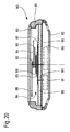
- FIG 20 is a sectional view of a watch 80 comprising a box 81, a bottom 82 and a glass 83.
- the watch 80 has a dielectric substrate 85, a plane of earth 86 connected to the box 81, a conductive element 87 and a frequency adjustment plate 88, the latter being separated from the conductive element 87 by another dielectric substrate 89.
- the conductive element comprises two pairs of orthogonal slots. The length of one of pairs of slots is greater than the length of the other pair, to ensure circular polarization antenna 87.
- the rotation of an adjustment plate frequency 88 with respect to the conductive element 87 modifies the lengths of the two pairs of orthogonal slots and, therefore, changes the resonant frequency of antenna 84.
- Watch 80 also includes a coaxial cable 90 whose central conductor crosses the substrate dielectric 85. This central conductor is soldered to the conductive element 87, while the external conductor is soldered to ground plane 86. The two conductors of the coaxial cable are also connected to an antenna circuit 91, arranged in watch 80, between the back 82 and the plane mass 86.
- watch 80 has a central support 92 on which the hour and minute hands are mounted and seconds, respectively 93, 94 and 95.
- the support central 92 is connected to a watch movement 96 which is also arranged between the bottom 82 and the ground plane 86.
- the watch movement 96 turns the hands 93 to 95 of watch 80 via the central support 92 to indicate the standard time.
- the central support 92 serves to maintain the alignment various elements 85 to 88 of the antenna 80.
- the environment close to antenna 80 has a certain effect on the resonant frequency of the antenna.
- the angular positions of the needles 93 to 95 by compared to the slots of the conductive member 87 have a some effect on the resonant frequency of the antenna.
- the hands 93 to 95 are brought by the watch movement 96 in angular positions that have little influence on the resonant frequency of the antenna 80.
- these angular positions are such that none of the needles 93 to 95 are superimposed on the slots of the conductive member 87.
- the needles 93 to 95 can be brought in the same positions angular during each reception / transmission, so that the influence of needles 93 to 95 on the frequency of resonance of antenna 80 is always the same.
- the frequency adjustment structures of resonance of the antenna which have just been described, allow on the one hand, compensation for the non homogeneity of the characteristics of the substrate material, and, on the other hand, a frequency adjustment on a band large.
- the dimensions of the antenna remain minimum because the frequency adjustment structures only slightly increase the thickness of the antenna.
Description
La présente invention est relative aux antennes destinées à convertir une tension alternative en une micro-onde et vice-versa et, plus particulièrement, à des antennes de ce type comprenant un élément conducteur et un plan de masse séparés par un substrat diélectrique. Ces antennes sont aussi connues sous l'appellation anglaise "microstrip patch antennas". L'invention peut être utilisée pour émettre et/ou recevoir des signaux GPS ("Global Positioning System"), et, en outre, elle peut être incorporée dans des montres ou d'autres produits horlogers. On décrira donc l'invention dans le cadre de cet exemple d'application. Toutefois, on comprendra que l'invention n'est bien entendu pas limitée à cette application.The present invention relates to antennas intended for convert an alternating voltage into a microwave and vice versa and, more particularly, to antennas of this type comprising a separate conductive element and a ground plane by a dielectric substrate. These antennas are also known under the English name "microstrip patch antennas". The invention can be used to transmit and / or receive GPS signals ("Global Positioning System"), and, moreover, it can be incorporated into watches or other products watchmakers. The invention will therefore be described in the context of this application example. However, it will be understood that the invention is of course not limited to this application.
La miniaturisation des antennes du type décrit ci-dessus est généralement accomplie en utilisant un substrat d'une permittivité très grande. Ceci implique invariablement l'utilisation d'un substrat en céramique. Les coûts de fabrication d'un tel substrat sont souvent élevés.The miniaturization of the antennas of the type described above is usually accomplished by using a substrate of a very high permittivity. This invariably involves the use of a ceramic substrate. The costs of manufacture of such a substrate are often high.
Une antenne miniaturisée est connue de la demande de brevet EP-A-0 525 726. Ce document décrit une antenne à polarisation circulaire comprenant un substrat diélectrique ayant deux faces opposées. Sur une face est fixé un plan de masse et sur l'autre face est fixé un élément conducteur. Cet élément conducteur est pourvu d'un point d'excitation électrique décentré par rapport à l'axe de rotation de l'antenne. Il est également pourvu de fentes placées à sa périphérie et passant virtuellement par son centre. Les caractéristiques de ces fentes, telles que leur longueur ou leur positionnement à la périphérie de l'élément conducteur, permettent de déterminer la fréquence de résonance de l'antenne. A miniaturized antenna is known from the patent application EP-A-0 525 726. This document describes a polarized antenna circular comprising a dielectric substrate having two opposite sides. On one side is fixed a ground plane and on the other side is fixed a conductive element. This element conductor is provided with an electrical excitation point off-center with respect to the axis of rotation of the antenna. It is also provided with slots placed at its periphery and passing virtually through its center. The characteristics of these slots, such as their length or positioning at the periphery of the conductive element, used to determine the resonant frequency of the antenna.
Une autre antenne de ce type est également connue de la publication IEEE Transactions on vehicular technology, vol.40, no.2, Mai 1991, New York US pages 483-486, intitulée « A flat energy density antenna system for mobile telephone ». Cette publication décrit également l'utilisation de fentes permettant notamment d'augmenter la fréquence de résonance de l'antenne en réduisant le rayon efficace de l'élément conducteur, c'est-à-dire en diminuant la longueur des fentes utilisées.Another antenna of this type is also known from the publication IEEE Transactions on vehicular technology, vol.40, no.2, May 1991, New York US pages 483-486, entitled "A flat energy density antenna system for mobile telephone ”. This publication also describes the use of slots allowing in particular to increase the resonant frequency of the antenna by reducing the effective radius of the element conductor, i.e. by reducing the length of the slots used.
Les antennes miniaturisées de ce type possèdent une largeur de bande très étroite. Par conséquent, en vertu des tolérances de fabrication, la conception et la construction de ces antennes est une tâche difficile. L'ajustement mécanique des bords de l'élément conducteur est une technique utilisée depuis longtemps pour obtenir la fréquence de résonance de l'antenne désirée. Cependant, une telle solution est à la fois destructrice et encombrante.Miniature antennas of this type have a width very narrow band. Therefore, under tolerances manufacturing, design and construction of these antennas is a difficult task. The mechanical adjustment of edges of the conductive element is a technique used long time to get the resonant frequency of the desired antenna. However, such a solution is both destructive and cumbersome.
La présente invention a pour but de fournir une antenne miniaturisée du type défini ci-dessus qui remédie tout au moins en partie aux inconvénients des antennes de l'état de l'art antérieur.The object of the present invention is to provide an antenna miniaturized of the type defined above which remedies everything less in part to the disadvantages of state antennas prior art.
Un autre but de l'invention est de fournir une antenne miniaturisée du type défini ci-dessus qui soit compacte, et qui soit relativement facile et peu coûteuse à fabriquer.Another object of the invention is to provide an antenna miniaturized of the type defined above which is compact, and which is relatively easy and inexpensive to manufacture.
En particulier, un but de l'invention est de fournir une antenne miniaturisée du type défini ci-dessus qui permette un réglage simple de sa fréquence de résonance.In particular, an object of the invention is to provide a miniaturized antenna of the type defined above which allows a simple adjustment of its resonant frequency.
Un autre but de l'invention est de fournir une antenne miniaturisée du type défini ci-dessus qui soit apte à être utilisée dans une montre.Another object of the invention is to provide an antenna miniaturized of the type defined above which is capable of being used in a watch.
A cet effet, l'invention a donc pour objet une antenne destinée à convertir une tension alternative, provenant d'un circuit d'antenne, en une onde à polarisation linéaire et vice versa, dont les caractéristiques sont énoncées à la revendication 1.To this end, the invention therefore relates to an antenna intended to convert an alternating voltage, coming from a antenna circuit, in a wave with linear polarization and vice versa, the characteristics of which are set out in claim 1.
L'invention a aussi pour objet une antenne destinée à
convertir une tension alternative provenant d'un circuit
d'antenne, en une onde à polarisation linéaire ou circulaire
et vice-versa, dont les caractéristiques sont énoncées à la
revendication 8.The invention also relates to an antenna intended for
convert alternating voltage from a circuit
antenna, in a wave with linear or circular polarization
and vice versa, the characteristics of which are set out in
Grâce à ces caractéristiques, l'invention permet la réalisation d'une antenne miniaturisée sans exiger l'utilisation d'un substrat d'une permittivité très élevée.Thanks to these characteristics, the invention allows the creation of a miniaturized antenna without requiring the use of a very high permittivity substrate.
Selon l'invention, l'antenne comprend une plaque de réglage de fréquence, montée sur le centre de l'élément conducteur et sur un axe perpendiculaire au plan de l'élément conducteur, la distance entre la périphérie et le centre de la plaque, le long de l'axe où s'étendent les fentes, étant variable de telle sorte que, par rotation, la plaque de réglage de fréquence agit de manière à modifier la longueur effective des fentes.According to the invention, the antenna comprises an adjustment plate frequency, mounted on the center of the conductive element and on an axis perpendicular to the plane of the conductive element, the distance between the periphery and the center of the plate, the along the axis where the slots extend, being variable by so that, by rotation, the adjustment plate frequency acts to modify the effective length of the slots.
Grâce à ces caractéristiques, la rotation de la plaque de réglage de fréquence autour de son axe permet, un réglage simple et précis de la fréquence de résonance de l'antenne, et ceci sur une largeur de bande plus grande que la largeur de bande de l'élément conducteur.Thanks to these characteristics, the rotation of the plate frequency adjustment around its axis allows, an adjustment simple and precise antenna resonant frequency, and this over a bandwidth greater than the width of conductive element strip.
D'autres caractéristiques et avantages de l'invention apparaítront au cours de la description qui va suivre, donnée uniquement à titre d'exemple, et faite en se référant aux dessins annexés dans lesquels:
- la figure 1 est une vue en coupe d'une antenne selon la présente invention;
- la figure 2 est une vue en perspective de l'antenne de la figure 1;
- la figure 3 est une vue en plan de l'élément conducteur de l'antenne des figures 1 et 2;
- la figure 4 est une vue en plan d'une variante de réalisation de l'élément conducteur de la figure 3;
- la figure 5 est une vue en plan d'une plaque de réglage de fréquence destinée à régler la fréquence de résonance de l'antenne de la figure 1;
- la figure 6 est une première variante de réalisation de la plaque de réglage de fréquence de la figure 5;
- la figure 7 est une deuxième variante de réalisation de la plaque de réglage de fréquence de la figure 5;
- la figure 8 est une troisième variante de réalisation de la plaque de réglage de fréquence de la figure 5;
- la figure 9 est une vue éclatée et en perspective d'une autre antenne selon l'invention;
- la figure 10 est une vue en coupe de l'antenne de la figure 9;
- la figure 11 est une vue en plan d'une autre variante de réalisation de l'élément conducteur de l'invention;
- la figure 12 est une vue en plan d'une autre variante de réalisation de l'élément conducteur de l'invention;
- la figure 13 est un vue en plan d'une autre variante de réalisation de la plaque de réglage de fréquence de la figure 5;
- la figure 14 est un vue en plan d'une autre variante de réalisation de la plaque de réglage de fréquence de la figure 5;
- la figure 15 est un vue en plan d'une autre variante du plaque de réglage de fréquence de la figure 5 ;
- la figure 16 est une vue en plan de l'agencement de la plaque de réglage de fréquence de la figure 13 et de l'élément conducteur de la figure 12;
- la figure 17 est une vue en plan de l'agencement de la plaque de réglage de fréquence de la figure 15 et de l'élément conducteur de la figure 11;
- la figure 18 est une vue en plan de l'agencement des plaques de réglage de fréquence des figures 7 et 8 et de l'élément conducteur de la figure 4;
- la figure 19 est une vue en plan de l'agencement de la plaque de réglage de fréquence de la figure 5 et de l'élément conducteur de la figure 3; et
- la figure 20 est une vue en coupe d'une montre comportant une antenne selon la présente invention.
- Figure 1 is a sectional view of an antenna according to the present invention;
- Figure 2 is a perspective view of the antenna of Figure 1;
- Figure 3 is a plan view of the conductive element of the antenna of Figures 1 and 2;
- Figure 4 is a plan view of an alternative embodiment of the conductive member of Figure 3;
- Figure 5 is a plan view of a frequency adjustment plate for adjusting the resonant frequency of the antenna of Figure 1;
- Figure 6 is a first alternative embodiment of the frequency adjustment plate of Figure 5;
- Figure 7 is a second alternative embodiment of the frequency adjustment plate of Figure 5;
- Figure 8 is a third alternative embodiment of the frequency adjustment plate of Figure 5;
- Figure 9 is an exploded perspective view of another antenna according to the invention;
- Figure 10 is a sectional view of the antenna of Figure 9;
- Figure 11 is a plan view of another alternative embodiment of the conductive element of the invention;
- Figure 12 is a plan view of another alternative embodiment of the conductive element of the invention;
- Figure 13 is a plan view of another alternative embodiment of the frequency adjustment plate of Figure 5;
- Figure 14 is a plan view of another alternative embodiment of the frequency adjustment plate of Figure 5;
- Figure 15 is a plan view of another variant of the frequency adjustment plate of Figure 5;
- Figure 16 is a plan view of the arrangement of the frequency adjustment plate of Figure 13 and the conductive member of Figure 12;
- Figure 17 is a plan view of the arrangement of the frequency adjustment plate of Figure 15 and the conductive member of Figure 11;
- Figure 18 is a plan view of the arrangement of the frequency adjustment plates of Figures 7 and 8 and of the conductive member of Figure 4;
- Figure 19 is a plan view of the arrangement of the frequency adjustment plate of Figure 5 and the conductive member of Figure 3; and
- Figure 20 is a sectional view of a watch comprising an antenna according to the present invention.
L'agencement de l'antenne miniaturisée 1 selon
l'invention représentée aux figures 1 et 2 comprend un
substrat diélectrique 2, un élément conducteur 3 et un
plan de masse 4. L'élément conducteur 3 a la forme
générale d'un disque et selon la dénomination anglo-saxonne
est appelé "radiating patch". L'élément conducteur
3 et le plan de masse 4 sont déposés sur des surfaces
opposées du substrat diélectrique 2. L'antenne 1 a une
géométrie apte à recevoir et émettre des ondes à
polarisation linéaire.The arrangement of the miniaturized antenna 1 according to
the invention shown in Figures 1 and 2 includes a
L'élément conducteur 3 comporte des fentes 5 et 6
diamétralement opposées et alignées selon l'axe 7. Ces
fentes 5 et 6 s'étendent à partir de la périphérie vers le
centre de l'élément conducteur 3. Un point d'excitation 8
est situé dans le plan de l'élément conducteur 3, sur un
axe 9 qui est perpendiculaire à l'axe 7. L'excitation est
assurée au moyen d'un câble coaxial dont le conducteur
central 10 traverse le substrat 2 et est soudé à l'élément
conducteur 3 à l'endroit du point d'excitation 8.The
La figure 3 montre plus précisément la géométrie de
l'élément conducteur 3. On voit que les fentes 5 et 6 ont
toutes deux une longueur rx et que l'élément conducteur 3
a un diamètre 2R, R étant le rayon de ce dernier.FIG. 3 shows more precisely the geometry of the
Les fentes 5 et 6 constituent une charge capacitive
pour l'antenne 1. Des considérations théoriques, qui ne
seront pas reprises ici car elles dépassent le cadre de la
présente demande de brevet, montrent que la fréquence de
résonance de l'antenne 1 dépend fortement de la longueur
rx des fentes 5 et 6. Selon ces considérations, lorsque rx
est nul, l'antenne 1 résonne à une fréquence fc. Mais,
lorsque la valeur de rx s'approche de R, la fréquence de
résonance s'approche de fc/2. On sait par ailleurs que le
diamètre 2R de l'antenne est une fonction de l'inverse de
la fréquence de résonance fc de celle-ci. Puisque la
fréquence de résonance fc est proche de fc/2 pour une
certaine dimension 2R, on peut également choisir de
réduire la dimension 2R de moitié pour une certaine
fréquence de résonance fc. C'est-à-dire, on peut diminuer
la dimension maximale de l'antenne 1 d'un facteur de 2
lorsque les fentes s'étendent sensiblement sur toute la
distance séparant la périphérie du centre dudit élément
conducteur. On notera à ce propos que les fentes 5 et 6
peuvent être réalisées par découpage de l'élément
conducteur 3 au moyen d'un faisceau laser. Bien entendu
les fentes 5 et 6 peuvent être également être réalisées
par gravage ou tout autre traitement chimique ou mécanique
de l'élément conducteur 3.The
Il faut noter que la forme circulaire de l'élément
conducteur 3 des figures 2 et 3 ne représente qu'un
exemple d'une forme de l'élément conducteur de
l'invention. Une forme carrée peut également être
utilisée, ainsi que tout autre élément conducteur qui est
délimité à sa périphérie par un bord qui confère à cet
élément une double symétrie planaire selon deux axes
perpendiculaires.Note that the circular shape of the
Dans le cas d'une antenne à polarisation linéaire, le
point d'excitation se trouve sur un des deux axes de
symétrie de l'élément conducteur et les fentes 5 et 6
s'étendent sur l'autre axe de symétrie.In the case of a linearly polarized antenna, the
excitation point is on one of the two axes of
symmetry of the conductive element and the
La figure 4 montre la géométrie d'un élément
conducteur 20 apte à recevoir et à émettre aussi bien des
signaux à polarisation circulaire que des signaux à
polarisation linéaire. L'élément conducteur 20 comporte
des fentes 21 et 22 qui s'étendent à partir de sa
périphérie vers le centre et qui sont alignées sur un même
axe 23. En outre, l'élément conducteur 20 comporte des
fentes 24 et 25 qui s'étendent à partir de sa périphérie
vers le centre et qui sont alignées sur un même axe 26
perpendiculaire à l'axe 23. Un point d'excitation 27 est
situé sur un axe décalé de 45° par rapport aux deux axes
23 et 24.Figure 4 shows the geometry of an
Pour que l'antenne ait une polarisation linéaire, les
longueurs rx des fentes 21 et 22 et ry des fentes 24 et 25
doivent être égales. Par contre, on obtient une
polarisation circulaire droite si, pour un point
d'excitation 27 tel que décrit ci-dessus, rx est supérieur
à ry selon un choix convenable. On comprendra que la forme
circulaire de l'élément conducteur 20 de la figure 4 ne
représente qu'une forme particulière de l'élément
conducteur de l'invention. Il va de soi qu'une forme
carrée peut être également utilisée ou encore tout autre
forme d'élément conducteur délimitée à sa périphérie par
un bord qui lui confère une double symétrie planaire selon
deux axes perpendiculaires. Dans le cas d'une antenne à
polarisation linéaire ou circulaire, comme, par exemple,
une antenne comportant l'élément conducteur 20 de la
figure 4, le point d'excitation 27 de l'élément conducteur
se trouve sur un axe bissecteur de l'angle formé entre les
deux axes de symétrie. Dans ce cas, les paires de fentes
21, 22 et 23, 24 s'étendent respectivement sur les deux
axes de symétrie.For the antenna to have a linear polarization, the lengths r x of the
La fréquence de résonance de l'antenne selon
l'invention varie en fonction de la distance r, si l'on
considère l'élément conducteur 3 de la figure 3, ou en
fonction des distances rx et ry, si l'on considère
l'élément conducteur montré à la figure 4. Comme on le
verra par la suite, en utilisant une ou plusieurs plaques
de réglage de fréquence de forme particulière comme couche
supérieure, on peut effectivement faire varier les
dimensions r, et le cas échéant les dimensions rx et ry,
par une simple rotation de cette plaque.The resonant frequency of the antenna according to the invention varies as a function of the distance r, if we consider the
Les figures 5, 6, 7 et 8 montrent respectivement des exemples 30, 31, 32 et 33 de géométries d'une telle plaque de réglage de fréquence, la distance entre la périphérie et le centre de ladite plaque, le long d'au moins un des axes définis par les fentes de l'élément conducteur, variant en fonction de l'angle de rotation de la plaque autour d'un axe perpendiculaire A au plan de la plaque et passant par le centre de la plaque par rapport à l'élément conducteur. Les structures montrées aux figures 5 à 8 peuvent être réalisées de plusieurs manières. Par exemple, elles peuvent être imprimées sur un substrat diélectrique ou usinées à partir d'un bloc de métal. Plusieurs formes de plaques sont envisageables et le choix de celles-ci dépend de la plage d'accord nécessaire ainsi que de la finesse de l'accord.Figures 5, 6, 7 and 8 show respectively examples 30, 31, 32 and 33 of geometries of such a plate frequency adjustment, the distance between the periphery and the center of said plate, along at least one of axes defined by the slots of the conductive element, varying according to the angle of rotation of the plate about an axis perpendicular A to the plane of the plate and passing through the center of the plate relative to the element driver. The structures shown in Figures 5 to 8 can be done in several ways. For example, they can be printed on a dielectric substrate or machined from a metal block. Several forms of plates are possible and the choice of these depends on the necessary tuning range as well as the finesse of the agreement.
Un contact électrique avec la surface de l'élément conducteur n'est pas nécessaire car le principe consistant à faire varier la capacité à travers les fentes fonctionne également lorsque le plaque et l'élément conducteur sont isolés l'un de l'autre. Aussi, si l'on désire conserver un contact électrique, le contact doit être uniforme sur toutes les fentes ce qui complique la conception de la plaque de réglage de fréquence. En conséquence, il est plus facile d'obtenir une isolation en utilisant une plaque diélectrique ou un entrefer entre la plaque de réglage de fréquence et les fentes de l'élément conducteur. De plus, on notera que dans ce cas la fréquence de résonance est moins sensible aux variations de rx et ry.Electrical contact with the surface of the conductive element is not necessary since the principle of varying the capacitance through the slots also works when the plate and the conductive element are isolated from each other. Also, if one wishes to maintain an electrical contact, the contact must be uniform on all the slots, which complicates the design of the frequency adjustment plate. As a result, it is easier to obtain insulation by using a dielectric plate or an air gap between the frequency adjustment plate and the slots of the conductive element. In addition, it will be noted that in this case the resonant frequency is less sensitive to the variations of r x and r y .
Les figures 9 et 10 montrent une antenne 40
comportant un substrat diélectrique 41, un plan de masse
42, un élément conducteur 43 et une plaque de réglage de
fréquence 44, cette dernière étant séparée de l'élément
conducteur 43 par un autre substrat diélectrique 45.
L'élément conducteur 43 comporte des fentes orthogonales
46, 47, 48 et 49. La rotation de la plaque de réglage de
fréquence 44 autour de l'axe A par rapport à l'élément
conducteur 43 modifie les longueurs effectives des fentes
46 à 49 et, par conséquent, modifie la fréquence de
résonance de l'antenne 40.Figures 9 and 10 show an
L'antenne 40 comporte en outre un connecteur coaxial
dont le conducteur central 50 passe à travers le substrat
41. Le conducteur central. 50 est soudé à l'élément
conducteur 43, tandis que le conducteur externe est soudé
au plan de masse 42. Les deux conducteurs du connecteur
coaxial sont également reliés à un circuit d'antenne.
L'antenne 40 convertit une tension alternative provenant
du circuit d'antenne, entre les deux conducteurs du
connecteur coaxial, en une micro-onde et vice-versa.The
De plus, l'antenne 40 comporte un support central 51
qui passe par des ouvertures 52, 53 et 54 au centre de la
structure montrée à la figure 9 et qui maintient
l'alignement des divers éléments de l'antenne 40. Le
support central 51 peut être réalisé soit en matière
isolante soit en matière conductrice, la différence liée à
l'utilisation de l'une ou l'autre de ces deux matières
étant un faible changement de la fréquence de résonance.
Cette différence peut être compensée de toute façon par
une rotation de la plaque de réglage de fréquence 44.In addition, the
On notera que le centre de l'élément conducteur 43
est un point de tension nul et que le fait que ce point
soit en circuit ouvert ou en court-circuit avec la masse
n'affecte pas les caractéristiques de l'antenne. On
utilisera de préférence, un support central métallique,
car dans ce cas le potentiel électrostatique de l'élément
conducteur 43 et celui de la plaque de réglage de
fréquence 44 sont à la masse. Ceci peut être avantageux du
point de vue de la compatibilité électromagnétique de
l'antenne 40.Note that the center of the
Lorsque la longueur rx des fentes 21 et 22 et la
longueur ry des fentes 24 et 25 de la figure 4 sont
égales, l'élément conducteur 20 est polarisé linéairement
le long d'une ligne passant par le centre de l'élément
conducteur 20 et par le point d'excitation 27. En
utilisant une plaque de réglage de fréquence comme cela
est représenté à la figure 7 ou à la figure 9, on peut
régler cette polarisation linéaire.When the length r x of the
Cependant, une polarisation circulaire de l'antenne
ayant un seul point d'excitation exige l'introduction
d'une asymétrie dans l'élément conducteur 20 afin que deux
modes orthogonaux de résonance soient établis. Une manière
de le faire consiste à introduire des segments de
perturbations dans l'élément conducteur 20. Divers
exemples de la forme de ces segments de perturbations sont
représentés par les références 60, 61, 62 et 63 des
éléments conducteurs 64 et 65 aux figures 11 et 12.
Ensuite, ces segments de perturbations 60 à 63 peuvent
être coupés pour introduire l'asymétrie désirée.However, circular polarization of the antenna
having a single point of excitement requires introduction
of an asymmetry in the
Dans certaines applications, le réglage de la
fréquence de résonance d'une antenne n'est requis que pour
surmonter l'incertitude de la valeur de la permittivité du
substrat. Dans ces cas, l'antenne peut être réglée en
utilisant les segments de perturbations qui viennent
d'être décrits. Des plaques de réglage de fréquence
simples à bande étroite peuvent être utilisées pour que
l'antenne puisse être accordée sur une fréquence désirée.
Les figures 13, 14 et 15 montrent des exemples de forme
des plaques 70, 71 et 72. La figure 16 montre l'agencement
de la plaque de réglage de fréquence 70 de la figure 13 et
de l'élément conducteur 65 de la figure 12. La figure 17
montre l'agencement de la plaque de réglage de fréquence
72 de la figure 15 et de l'élément conducteur 64 de la
figure 11. On remarquera que la forme et la taille des
plaques de réglage de fréquence 70, 71 et 72 par rapport
aux éléments conducteurs correspondants sont telles que la
distance entre la périphérie et le centre des plaques 70,
71 et 72 varie peu en fonction de l'angle de rotation.In some applications, adjusting the
resonant frequency of an antenna is only required for
overcome the uncertainty of the value of the permittivity of the
substrate. In these cases, the antenna can be adjusted by
using the disturbance segments that come
to be described. Frequency adjustment plates
simple narrow band can be used so that
the antenna can be tuned to a desired frequency.
Figures 13, 14 and 15 show examples of
Cette asymétrie peut être également introduite, dans
le cas où la structure de l'antenne est telle que les
longueurs des fentes rx et ry ont la même valeur, en
utilisant une combinaison de deux plaques de réglage de
fréquence. La figure 18 montre un exemple d'une telle
combinaison de plaques. Dans cet exemple, les plaques de
réglage de fréquence 32 et 33, respectivement montrées aux
figures 7 et 8, sont supportées au-dessus de l'élément
conducteur 20 de la figure 4. On peut tout d'abord faire
tourner le plaque de réglage de fréquence 32 pour établir
une polarisation linéaire à une fréquence désirée.
Ensuite, la plaque de réglage de fréquence 33 peut être
tournée pour introduire un décalage contrôlé entre les
dimensions rx et ry, ce qui conduit l'antenne à un
fonctionnement à polarisation circulaire. Avantageusement,
l'utilisation de deux plaques de réglage de fréquence
permet de pouvoir prévoir des tolérances de fabrication de
l'antenne plus larges.This asymmetry can also be introduced, in the case where the structure of the antenna is such that the lengths of the slots r x and r y have the same value, by using a combination of two frequency adjustment plates. Figure 18 shows an example of such a combination of plates. In this example, the
Cette description va maintenant être complétée en se référant à des exemples pratiques de construction d'une antenne selon l'invention. Puisque les antennes étaient conçues en utilisant un plan numérique qui divise la surface de l'élément conducteur en cellules carrées, les dimensions exprimées dans ces exemples sont dans les termes de "taille de cellule Δ".This description will now be completed by referring to practical examples of building a antenna according to the invention. Since the antennas were designed using a digital plan that divides the surface of the conducting element in square cells, the dimensions expressed in these examples are in terms of "cell size Δ".
Un élément conducteur ayant la forme représentée à la
figure 3 est gravé à partir d'un substrat en un matériau
vendu sous la désignation commerciale ULTRALAM®. Les
dimensions initiales du substrat étaient de 144 x 1,5 mm3
et sa permittivité relative est de 2,5. Un trou circulaire
d'un diamètre de 1 mm est percé au centre du substrat.
L'antenne est excitée au moyen d'un signal appliqué sur
l'élément conducteur 3 via un câble coaxial standard 50 Ω
SMA. Les dimensions de l'élément conducteur sont les
suivantes :
Δ = 40/61 mm, 2R = 30,5 Δ, r = 19 Δ, w = 0,5 Δ, yf = 7 Δ.
En outre, un trou d'un diamètre égal à 3 Δ est formé au
centre de l'élément conducteur.A conductive element having the shape shown in FIG. 3 is etched from a substrate made of a material sold under the trade designation ULTRALAM®. The initial dimensions of the substrate were 144 x 1.5 mm 3 and its relative permittivity is 2.5. A circular hole with a diameter of 1 mm is drilled in the center of the substrate. The antenna is energized by means of a signal applied to the
Δ = 40/61 mm, 2R = 30.5 Δ, r = 19 Δ, w = 0.5 Δ, yf = 7 Δ.
In addition, a hole with a diameter equal to 3 Δ is formed in the center of the conductive element.
On a utilisé une plaque de réglage de fréquence ayant la forme représentée à la figure 5. L'agencement de l'antenne est représenté à la figure 19. La plaque de réglage de fréquence est gravée à partir d'un disque circulaire en époxy. On a choisi cette matière dans ce cas en raison de sa grande rigidité. Le disque circulaire a une épaisseur de 0,8 mm et un diamètre de 60 mm. On a également utilisé un autre disque en époxy tel que celui référencé 45 à la figure 9. Ce disque sert de plaque d'espacement entre l'élément conducteur et la plaque de réglage de fréquence. La plaque d'espacement a une épaisseur de 0,1 mm et un diamètre de 25 mm.A frequency adjustment plate was used having the shape shown in Figure 5. The arrangement of the antenna is represented in figure 19. The plate of frequency setting is burned from a disc circular in epoxy. We chose this material in this case due to its great rigidity. The circular disc has a thickness of 0.8 mm and a diameter of 60 mm. We have also used another epoxy disc such as that referenced 45 in Figure 9. This disc serves as a plate spacing between the conductive element and the plate frequency setting. The spacer plate has a thickness of 0.1 mm and a diameter of 25 mm.
On a mesuré la fréquence de résonance de l'antenne et on a constaté que cette fréquence variait entre 2,118 GHz (lorsque l'angle 1 = 90°) et 2,448 GHz (lorsque l'angle 1 = 0°). Cette variation correspond à une plage de réglage de la fréquence de 14,5%. Le rapport d'ondes stationnaires en tension, mesuré à la fréquence de résonance, est meilleur que 2 sur la totalité de la bande. Les diagrammes de rayonnement ont été mesurés dans une enceinte anechoïque à trois fréquences différentes, à savoir, 2,118, 2,296 et 2,448 GHz, ces trois fréquences correspondant respectivement à trois positions angulaires différentes de la structure de réglage de fréquence. Les diagrammes de co-polarisation sont dans ces cas sensiblement les mêmes que les diagrammes de co-polarisation pour un élément conducteur circulaire. De plus, les niveaux de polarisation croisée sont inférieurs à -20 dB, ce qui indique que la structure de réglage de fréquence n'introduit aucun niveau de rayonnement à polarisation croisée inacceptable.We measured the resonant frequency of the antenna and this frequency has been found to vary between 2.118 GHz (when the angle 1 = 90 °) and 2,448 GHz (when the angle 1 = 0 °). This variation corresponds to a range of frequency setting of 14.5%. The wave report stationary in voltage, measured at the frequency of resonance, is better than 2 over the entire band. The radiation patterns were measured in a anechoic enclosure at three different frequencies, namely, 2.118, 2.296 and 2.448 GHz, these three frequencies corresponding respectively to three angular positions different from the frequency adjustment structure. The co-polarization diagrams are in these cases much the same as the co-polarization diagrams for a circular conductive element. Of more, cross-polarization levels are lower at -20 dB, which indicates that the adjustment structure of frequency does not introduce any radiation level at unacceptable cross polarization.
On notera que l'angle de rotation de la plaque de
réglage de fréquence 33 de l'antenne représentée à la
figure 19 est limité à une valeur de 90°. Cependant,
l'utilisation de la plaque de réglage de fréquence
représentée à la figure 6 autorise une rotation d'un angle
de 180° et par conséquent un réglage plus fin de la
fréquence dans la même plage de fréquence.Note that the angle of rotation of the
On a fabriqué une antenne ayant un agencement tel que
celui représenté à la figure 18. Cette antenne a été
excitée en un seul point situé sur un axe bissecteur de
l'angle formé entre les deux axes orthogonaux des fentes
de l'élément conducteur. On sait que cette technique
d'excitation est assez sensible par rapport aux autres
techniques connues et qu'elle exige une séparation précise
entre les deux modes dégénérés de l'antenne. En
particulier, les deux fréquences de résonance doivent être
séparées d'une fréquence α où
Des expériences pratiques ont montré que la largeur de bande de l'antenne varie en fonction du réglage de la fréquence. Cette variation peut compliquer la conception d'une simple plaque de réglage de fréquence car une connaissance précise de son effet est requise. L'utilisation de deux plaques de réglage de fréquence, comme les deux plaques représentées à la figure 18, peut pallier ce problème. En outre, l'utilisation de deux plaques de réglage de fréquence permet de pouvoir prévoir des tolérances de fabrication de l'antenne plus larges.Practical experiences have shown that the width bandwidth varies depending on the setting of the frequency. This variation can complicate the design a simple frequency adjustment plate because a precise knowledge of its effect is required. The use of two frequency adjustment plates, like the two plates shown in figure 18, can alleviate this problem. In addition, the use of two frequency adjustment plates allows you to predict wider antenna manufacturing tolerances.
Dans cet exemple, l'élément conducteur est gravé à
partir d'un substrat en un matériau vendu sous la
désignation commerciale ULTRALAM®. Les dimensions
initiales du substrat étaient de 144 x 144 x 1,5 mm3 et sa
permittivité relative est de 2,5. Un trou circulaire d'un
diamètre de 1 mm est percé au centre du substrat.
L'antenne est excitée au moyen d'un signal appliqué sur
l'élément conducteur 3 via un câble coaxial standard 50 Ω
SMA. Les dimensions de l'élément conducteur sont les
suivantes :
Δ = 40/61 mm, 2R = 30,5 Δ, rx = ry = 19 Δ, w = 0,5 Δ,
xf = yf = 7 Δ.
En outre, un trou d'un diamètre égal à 3 Δ est prévu au
centre de l'élément conducteur.In this example, the conductive element is etched from a substrate made of a material sold under the trade designation ULTRALAM®. The initial dimensions of the substrate were 144 x 144 x 1.5 mm 3 and its relative permittivity is 2.5. A circular hole with a diameter of 1 mm is drilled in the center of the substrate. The antenna is energized by means of a signal applied to the
Δ = 40/61 mm, 2R = 30.5 Δ, r x = r y = 19 Δ, w = 0.5 Δ,
x f = y f = 7 Δ.
In addition, a hole with a diameter equal to 3 Δ is provided in the center of the conductive element.
Des plaques de réglage de fréquence ayant la forme
représentée aux figures 7 et 8 sont utilisées.
L'agencement de l'antenne est représenté à la figure 18.
La plaque de réglage de fréquence de la figure 7 est
gravée à partir d'un disque circulaire en époxy. Le disque
circulaire a une épaisseur de 0,1 mm et un diamètre de
60 mm. La plaque de réglage de fréquence de la figure 8
est également gravée à partir d'un disque circulaire en
époxy. Le disque circulaire a une épaisseur de 0,8 mm et
un diamètre de 50 mm. Un autre disque en époxy, comme
celui désigné par la référence numérique 45 à la figure 9,
est utilisé comme plaque d'espacement et est disposé entre
l'élément conducteur et la plaque de réglage de fréquence.
La plaque d'espacement a une épaisseur de 0,1 mm et un
diamètre de 25 mm. Aucun disque d'espacement n'est utilisé
entre les deux plaques de réglage de fréquence.Frequency adjusting plates having the form
shown in Figures 7 and 8 are used.
The antenna layout is shown in Figure 18.
The frequency adjustment plate of figure 7 is
engraved from a circular epoxy disc. The disc
circular has a thickness of 0.1 mm and a diameter of
60 mm. The frequency adjustment plate of figure 8
is also engraved from a circular disc in
epoxy. The circular disc has a thickness of 0.8 mm and
a diameter of 50 mm. Another epoxy disc, like
that designated by the
La gamme de réglage de la fréquence de résonance de l'antenne est légèrement inférieure à la gamme de réglage de l'exemple précédent en raison du décalage entre les deux modes dégénérés de l'antenne dans le deuxième exemple. Cette variation est de l'ordre de 10%. Le rapport d'ondes stationnaires en tension, mesuré à la résonance, est meilleur que 2 à une fréquence de 2,306 MHz.The range of adjustment of the resonant frequency of the antenna is slightly lower than the adjustment range from the previous example due to the lag between two degenerate modes of the antenna in the second example. This variation is around 10%. The report standing waves in tension, measured at resonance, is better than 2 at a frequency of 2.306 MHz.
Alors que l'agencement montré à la figure 18 engendre
une polarisation circulaire à droite, on notera que la
rotation de la plaque 33 d'un angle de 90° engendre une
polarisation circulaire à gauche. While the arrangement shown in Figure 18 creates
a circular polarization on the right, it will be noted that the
rotation of the
On grave à partir d'un substrat en un matériau vendu
sous la désignation commerciale TMM-10® un élément
conducteur ayant la forme représentée à la figure 11, cet
élément conducteur comportant des segments de
perturbations permettant un fonctionnement à polarisation
circulaire à droite. Le substrat est circulaire et a un
diamètre de 34,5 mm. L'épaisseur du substrat est de
0,635 mm et sa permittivité relative est de 9,2. Un trou
circulaire d'un diamètre de 1,4 mm est percé au centre du
substrat. L'antenne est excitée au moyen d'un signal
appliqué sur l'élément conducteur via un câble coaxial
standard 50 Ω SMA. Les dimensions de l'élément conducteur
sont les suivantes:
2R = 14,75 mm, rx = ry = 9,5 mm, w = 0,25 mm,
xf = yf = 3,5 mm.
En outre, un trou d'un diamètre égal à 1,693 mm est percé
au centre de l'élément conducteur.A conductive element having the shape shown in FIG. 11 is etched from a substrate made of a material sold under the trade name TMM-10®, this conductive element comprising disturbance segments allowing operation with circular polarization to the right. The substrate is circular and has a diameter of 34.5 mm. The thickness of the substrate is 0.635 mm and its relative permittivity is 9.2. A circular hole with a diameter of 1.4 mm is drilled in the center of the substrate. The antenna is energized by means of a signal applied to the conductive element via a standard 50 Ω SMA coaxial cable. The dimensions of the conductive element are as follows:
2R = 14.75 mm, r x = r y = 9.5 mm, w = 0.25 mm,
x f = y f = 3.5 mm.
In addition, a hole with a diameter equal to 1.693 mm is drilled in the center of the conductive element.
On a utilisé une plaque de réglage de fréquence ayant la forme représentée à la figure 15. L'agencement de l'antenne est représenté à la figure 17. La plaque de réglage de fréquence est gravée à partir d'un disque circulaire en époxy. Cette matière est préférée ici en raison de sa grande rigidité. Le disque circulaire a une épaisseur de 0,8 mm et un diamètre de 25 mm. Un disque diélectrique en TEFLON® est utilisé comme plaque d'espacement et est disposé entre l'élément conducteur et la plaque de réglage de fréquence. La plaque d'espacement a une épaisseur de 0,254 mm et un diamètre de 25 mm. Cette structure permet d'obtenir une gamme de réglage de fréquence de l'ordre de 2 %. A frequency adjustment plate was used having the shape shown in Figure 15. The arrangement of the antenna is represented in figure 17. The plate of frequency setting is burned from a disc circular in epoxy. This material is preferred here in because of its great rigidity. The circular disc has a 0.8 mm thick and 25 mm in diameter. A disk TEFLON® dielectric is used as a plate and is arranged between the conductive element and the frequency adjustment plate. The spacer plate has a thickness of 0.254 mm and a diameter of 25 mm. This structure provides a range of adjustment frequency of the order of 2%.
L'antenne est réglée à la fréquence des signaux GPS (1,57542 GHz) par la rotation de la plaque de réglage de fréquence. Le rapport axial mesuré est de 2,54 dB et la largeur de bande, avec un rapport d'ondes stationnaires en tension égale à 2, est de 12 MHz. Le gain mesuré est de -6 dBi.The antenna is adjusted to the frequency of GPS signals (1.57542 GHz) by the rotation of the adjustment plate frequency. The measured axial ratio is 2.54 dB and the bandwidth, with a standing wave ratio in voltage equal to 2, is 12 MHz. The gain measured is -6 dBi.
Cet exemple utilise un élément conducteur comprenant
des segments de perturbations pour un fonctionnement à
polarisation circulaire à droite. Un élément conducteur
ayant la forme représentée à la figure 12 est gravé à
partir d'un substrat en TMM-10®. Le substrat est
circulaire et a un diamètre de 34,5 mm. L'épaisseur du
substrat est de 1,27 mm et sa permittivité relative est de
9,2. Un trou circulaire d'un diamètre de 1,4 mm est percé
au centre du substrat. L'antenne est excitée au moyen d'un
signal appliqué sur l'élément conducteur via un câble
coaxial standard 50 Ω SMA. Les dimensions de l'élément
conducteur sont les suivantes :
2R = 14,7 mm, rx = ry = 10,12 mm, w = 0,25, et
xf = yf = 1,93 mm.
En outre, un trou d'un diamètre égal à 1,631 mm est percé
au centre de l'élément conducteur.This example uses a conductive element comprising disturbance segments for operation with right-hand circular polarization. A conductive element having the shape shown in FIG. 12 is etched from a TMM-10® substrate. The substrate is circular and has a diameter of 34.5 mm. The thickness of the substrate is 1.27 mm and its relative permittivity is 9.2. A circular hole with a diameter of 1.4 mm is drilled in the center of the substrate. The antenna is energized by means of a signal applied to the conductive element via a standard 50 Ω SMA coaxial cable. The dimensions of the conductive element are as follows:
2R = 14.7 mm, r x = r y = 10.12 mm, w = 0.25, and
x f = y f = 1.93 mm.
In addition, a hole with a diameter equal to 1.631 mm is drilled in the center of the conductive element.
Une plaque de réglage de fréquence ayant la forme représentée à la figure 13 est usinée à partir d'un bloc de cuivre. Aucun disque d'espacement n'est utilisé, mais un entrefer est créé en supportant la plaque de réglage de fréquence à 0,2 mm au-dessus de l'élément conducteur au moyen d'un élément de support central. L'agencement de l'antenne est illustré à la figure 16.A frequency adjustment plate having the form shown in figure 13 is machined from a block of copper. No spacer disc is used, but an air gap is created by supporting the adjustment plate frequency 0.2 mm above the conductive element at by means of a central support element. The layout of the antenna is illustrated in Figure 16.
Dans cet exemple, on peut faire tourner la plaque de réglage de fréquence de 90° pour obtenir une gamme de réglage de fréquence de 6%. La géométrie de la plaque de réglage de fréquence 70 est telle que la distance entre sa périphérie et son origine varie linéairement entre 4,5 mm et 8,75 mm en fonction de l'angle de rotation de celle-ci.In this example, you can rotate the 90 ° frequency adjustment to obtain a range of frequency setting of 6%. The plate geometry frequency setting 70 is such that the distance between its periphery and its origin varies linearly between 4.5 mm and 8.75 mm depending on the angle of rotation thereof.
L'antenne de cet exemple est montée dans un boítier en plastique et est réglée à la fréquence des signaux GPS (1,57542 GHz) par rotation de la plaque de réglage de fréquence. Le rapport axial mesuré, avec le boítier fixé au plan de masse de l'antenne, est de 1,78 dB et la largeur de bande lorsque le rapport d'ondes stationnaires en tension est égale à 2 est de 11 MHz. Le gain mesuré est de -4,0 dB.The antenna in this example is mounted in a housing plastic and is set to the frequency of GPS signals (1.57542 GHz) by rotation of the adjustment plate frequency. The measured axial ratio, with the housing fixed at the antenna ground plane, is 1.78 dB and the bandwidth when the standing wave ratio in voltage is equal to 2 is 11 MHz. The gain measured is -4.0 dB.
Selon une variante de cet exemple de réalisation, la
plaque de réglage de fréquence 70 peut être remplacée par
la plaque de réglage de fréquence 71 de la figure 14.
Cette plaque de réglage de fréquence est plus facile à
fabriquer car elle peut être réalisée à partir de barres
parallélipédiques actuellement disponibles dans le
commerce. La gamme de réglage dans ce cas est de l'ordre
de 3 % et l'angle de rotation maximale est de 45°.According to a variant of this exemplary embodiment, the
L'invention permet un certain nombre d'applications intéressantes. D'abord, la géométrie de l'élément conducteur permet un contrôle convenable de sa taille. Des formes actuelles telles que des formes circulaires ou rectangulaires ont une taille fixe selon la fréquence de résonance désirée et selon les caractéristiques du substrat utilisé. En utilisant une longueur de fente variable, on peut modifier les dimensions de l'antenne d'un facteur 2. En outre, la forme de l'élément conducteur permet une utilisation optimale de la surface disponible, car il y a peu de surface non métallisée. En conséquence, l'invention permet une miniaturisation de l'antenne tout en gardant un rapport gain/taille optimal.The invention allows a number of applications interesting. First, the geometry of the element conductor allows proper size control. of the current shapes such as circular shapes or rectangular have a fixed size according to the frequency of desired resonance and according to the characteristics of the substrate used. Using a slot length variable, you can modify the antenna dimensions by a factor of 2. Furthermore, the shape of the conductive element allows optimal use of the available space, because there is little unmetallized surface. Consequently, the invention allows miniaturization of the antenna while keeping an optimal gain / size ratio.
Les exemples 3 et 4 ci-dessus décrivent des antennes qui sont destinées à recevoir, des ondes de signaux GPS transmis par satellite. Les dimensions de l'antenne sont telles qu'elle peut être montée dans une boíte de montre. Dans une montre, l'antenne peut être par exemple disposée entre le moteur et les aiguilles.Examples 3 and 4 above describe antennas which are intended to receive, waves of GPS signals transmitted by satellite. The dimensions of the antenna are as it can be mounted in a watch case. In a watch, the antenna can for example be arranged between the engine and the needles.
La figure 20 est une vue en coupe d'une montre 80
comportant une boíte 81, un fond 82 et un verre 83. La
montre 80 comporte un substrat diélectrique 85, un plan de
masse 86 relié à la boíte 81, un élément conducteur 87 et
une plaque de réglage de fréquence 88, cette dernière
étant séparée de l'élément conducteur 87 par un autre
substrat diélectrique 89. L'élément conducteur comporte
deux paires de fentes orthogonales. La longueur d'une des
paires de fentes est plus grande que la longueur de
l'autre paire, afin d'assurer une polarisation circulaire
de l'antenne 87. La rotation d'une plaque de réglage de
fréquence 88 par rapport à l'élément conducteur 87 modifie
les longueurs des deux paires de fentes orthogonales et,
par conséquent, modifie la fréquence de résonance de
l'antenne 84.Figure 20 is a sectional view of a
La montre 80 comporte en outre un câble coaxial 90
dont le conducteur central traverse le substrat
diélectrique 85. Ce conducteur central est soudé à
l'élément conducteur 87, tandis que le conducteur externe
est soudé au plan de masse 86. Les deux conducteurs du
câble coaxial sont également reliés à un circuit d'antenne
91, disposé dans la montre 80, entre le fond 82 et le plan
de masse 86.
De plus, la montre 80 comporte un support central 92
sur lequel sont montées les aiguilles d'heures, de minutes
et de secondes, respectivement 93, 94 et 95. Le support
central 92 est relié à un mouvement d'horlogerie 96 qui
est également disposé entre le fond 82 et le plan de masse
86. Le mouvement d'horlogerie 96 fait tourner les
aiguilles 93 à 95 de la montre 80 par l'intermédiaire du
support central 92 afin d'indiquer l'heure standard. En
outre, le support central 92 sert à maintenir l'alignement
des divers éléments 85 à 88 de l'antenne 80.In addition, watch 80 has a
L'environnement proche de l'antenne 80 a un certain
effet sur la fréquence de résonance de l'antenne. A cet
égard, les positions angulaires des aiguilles 93 à 95 par
rapport aux fentes de l'élément conducteur 87 ont un
certain effet sur la fréquence de résonance de l'antenne.
Pour compenser cet effet, lors de la réception ou de la
transmission d'un signal par l'antenne 80, les aiguilles
93 à 95 sont amenées par le mouvement d'horlogerie 96 dans
des positions angulaires qui ont peu d'influence sur la
fréquence de résonance de l'antenne 80.The environment close to
De préférence, ces positions angulaires sont telles
qu'aucune des aiguilles 93 à 95 ne sont superposées aux
fentes de l'élément conducteur 87. En outre, les aiguilles
93 à 95 peuvent être amenées dans les mêmes positions
angulaires lors de chaque réception/transmission, afin que
l'influence des aiguilles 93 à 95 sur la fréquence de
résonance de l'antenne 80 soit toujours la même.Preferably, these angular positions are such
that none of the
Les structures de réglage de la fréquence de résonance de l'antenne qui viennent d'être décrites, permettent d'une part, une compensation de la non homogénéité des caractéristiques du matériau du substrat, et, d'autre part, un réglage de fréquence sur une bande large. De plus, les dimensions de l'antenne restent minimum car les structures de réglage de fréquence n'augmentent que très légèrement l'épaisseur de l'antenne.The frequency adjustment structures of resonance of the antenna which have just been described, allow on the one hand, compensation for the non homogeneity of the characteristics of the substrate material, and, on the other hand, a frequency adjustment on a band large. In addition, the dimensions of the antenna remain minimum because the frequency adjustment structures only slightly increase the thickness of the antenna.
On notera que pour obtenir une telle taille avec une antenne circulaire connue, il est nécessaire d'utiliser un substrat ayant une permittivité relative de l'ordre de 15. Une telle permittivité nécessite l'utilisation d'un substrat en céramique et conduit à des frais de fabrication plus élevés. A noter en outre que ces substrats en céramique présentent des caractéristiques thermiques insuffisantes dans de nombreuses applications. Par exemple, l'environnement proche de l'antenne a un certain effet sur la fréquence de résonance de l'antenne. Cet effet peut être compensé par une simple rotation de la plaque de réglage de fréquence de l'antenne. A cet égard, les aiguilles d'une montre comportant l'antenne de l'invention sont, de préférence, réalisées en plastique, ou en toute autre matière non métallique, pour diminuer cet effet.Note that to obtain such a size with a known circular antenna, it is necessary to use a substrate having a relative permittivity of the order of 15. Such permittivity requires the use of a ceramic substrate and leads to costs of higher manufacturing. Also note that these ceramic substrates have characteristics insufficient thermal in many applications. For example, the environment near the antenna has a some effect on the resonant frequency of the antenna. This effect can be offset by a simple rotation of the antenna frequency adjustment plate. In this regard, clock hands with the antenna the invention are preferably made of plastic, or any other non-metallic material, to decrease this effect.
Claims (19)
- Antenna for converting an alternating voltage provided by an antenna circuit into a linearly polarised microwave and vice versa, comprising :said conductive element including an excitation point (8) by which it is connected to said antenna circuit, this latter providing said alternating voltage between the excitation point and said ground plane;a first dielectric substrate (2; 41) including two opposing sides;a conductive element (3) fixed on a first side of said first dielectric substrate, said conductive element being delimited at its periphery by an edge which confer to this element a double planar symmetry according to two perpendicular axes (7; 9); anda ground plane (4; 42) fixed to the second side of said first dielectric substrate;
said excitation point (8) being located on a first (9) of said axes (7; 9);
said conductive element (3) further including :said antenna being characterized in that it further includes:a first pair of slots (5, 6) which extend, along the second (7) of said axes (7, 9), from the periphery towards the center of said conductive element over substantially the entire distance separating the periphery from the center of said conductive element;a first frequency adjustment plate (30; 31; 32; 33; 44; 70; 71; 72) disposed on the center of said conductive element and on an axis perpendicular to the plane of said conductive element, the distance between the periphery and the center of said first plate, along said second axis, being variable so that, through rotation, said first frequency adjustment plate acts so as to modify the effective length of said slots (5, 6). - Antenna according to claim 1, characterized in that said frequency adjustment plate is machined from a block of metal.
- Antenna according to claim 1, characterized in that said frequency adjustment plate is printed on a second dielectric substrate.
- Antenna according to any one of claims 1 to 3, characterized in that it further comprises:a spacing disc (45) which separates said first conductive element from said frequency adjustment plate.
- Antenna according to any one of claims 1 to 3, characterized in that said frequency adjustment plate and said conductive element are separated by an air-gap.
- Antenna according to any one of the preceding claims, characterized in that it further comprises:a central support (51) which passes through said first dielectric substrate and said frequency adjustment plate, and on which these elements are mounted.
- Antenna according to claim 6, characterized in that said central support is manufactured from a conductive material.
- Antenna for converting an alternating voltage provided by an antenna circuit into a linearly or circularly polarised microwave and vice versa, comprising :said conductive element including an excitation point (27) by which it is connected to said antenna circuit, this latter providing said alternating voltage between the excitation point and said ground plane;a first dielectric substrate (2; 41) including two opposing sides;a first conductive element (20; 43; 64; 65) fixed on a first side of said first dielectric substrate, said conductive element being delimited at its periphery by an edge which confer to this element a double planar symmetry according to two perpendicular axes (23; 26); anda ground plane (4; 42) fixed to the second side of said first dielectric substrate;
said excitation point (27) being located on a third axis which bisectors the angle formed between the first and second axes (23; 26);
said conductive element (20; 43; 64; 65) further including :said antenna being characterized in that it further includes:a first pair of slots (21, 22; 46, 47) which extend, along said first axis (23), from the periphery towards the center of said conductive element over substantially the entire distance separating the periphery from the center of said conductive element; anda second pair of slots (24, 25; 48, 49) which extend, along said second axis (26), from the periphery towards the center of said conductive element over substantially the entire distance separating the periphery from the center of said conductive element;a first frequency adjustment plate (30; 31; 32; 33; 44; 70; 71; 72) disposed on the center of said conductive element and on an axis perpendicular to the plane of said conductive element, the distance between the periphery and the center of said first plate, along said second axis, being variable so that, through rotation, said first frequency adjustment plate acts so as to modify the effective length of said second pair of slots (24, 25; 48, 49). - Antenna according to claim 8, characterized in that the length of said first pair of slots (21, 22; 46, 47) is greater than the length of said second pair of slots (24, 25; 48, 49) to create said circular polarised microwaves.
- Antenna according to any one of claims 8 to 9, characterized in that the distance between the periphery and the center of said first frequency adjustment plate, along said first axis, is variable so that, through rotation, said first frequency adjustment plate acts so as to modify the effective length of said first pair of slots (21, 22; 46, 47).
- Antenna according to any one of claims 8 to 10, characterized in that it further comprises:a second frequency adjustment plate disposed on the center of said conductive element and on an axis perpendicular to the plane of said conductive element, the distance between the periphery and the center of said second plate, along said first axis, being variable so that, through rotation, said second frequency adjustment plate acts so as to modify the effective length of said first pair of slots (21, 22; 46, 47).
- Antenna according to any one of claims 8 to 11, characterized in that at least one of said frequency adjustment plates is machined from a block of metal.
- Antenna according to any one of claims 8 to 11, characterized in that at least one of said frequency adjustment plates is printed on a second dielectric substrate.
- Antenna according to any one of claims 8 to 13, characterized in that it further comprises:a spacing disc (45) which separates said conductive element from at least one of said frequency adjustment plates.
- Antenna according to any one of claims 8 to 13, characterized in that at least one of said frequency adjustment plates and said conductive element are separated by an air-gap.
- Antenna according to any one of claims 8 to 15, characterized in that it further comprises:a central support (51) which passes through the first dielectric substrate and at least one of said frequency adjustment plates, and on which these elements are mounted.
- Antenna according to claim 16, characterized in that said central support is realised in a conductive material.
- Watch comprising an antenna according to any one of claims 6 to 7 and 16 to 17, said watch comprising:said watch being characterized in thathands;a watch case;a motor; anda shaft for connecting said motor to said hands;
said antenna is located between said motor and said hands, in that said central support is hollowed along its longitudinal axis, and in that said shaft extends along the interior of said central support. - Watch according to claim 18, characterized in that said hands are realised in plastic.
Applications Claiming Priority (2)
| Application Number | Priority Date | Filing Date | Title |
|---|---|---|---|
| FR9412480 | 1994-10-19 | ||
| FR9412480A FR2726127B1 (en) | 1994-10-19 | 1994-10-19 | MINIATURIZED ANTENNA FOR CONVERTING AN ALTERNATIVE VOLTAGE TO A MICROWAVE AND VICE-VERSA, PARTICULARLY FOR WATCHMAKING APPLICATIONS |
Publications (2)
| Publication Number | Publication Date |
|---|---|
| EP0708492A1 EP0708492A1 (en) | 1996-04-24 |
| EP0708492B1 true EP0708492B1 (en) | 2002-06-12 |
Family
ID=9468001
Family Applications (1)
| Application Number | Title | Priority Date | Filing Date |
|---|---|---|---|
| EP95116148A Expired - Lifetime EP0708492B1 (en) | 1994-10-19 | 1995-10-13 | Microstrip patch antenna and its particular application in a timepiece |
Country Status (7)
| Country | Link |
|---|---|
| US (1) | US5646634A (en) |
| EP (1) | EP0708492B1 (en) |
| JP (1) | JPH08213819A (en) |
| AU (1) | AU695429B2 (en) |
| CA (1) | CA2159961A1 (en) |
| DE (1) | DE69527020T2 (en) |
| FR (1) | FR2726127B1 (en) |
Families Citing this family (46)
| Publication number | Priority date | Publication date | Assignee | Title |
|---|---|---|---|---|
| GB2337861B (en) * | 1995-06-02 | 2000-02-23 | Dsc Communications | Integrated directional antenna |
| FR2748162B1 (en) * | 1996-04-24 | 1998-07-24 | Brachat Patrice | COMPACT PRINTED ANTENNA FOR LOW ELEVATION RADIATION |
| FR2757315B1 (en) * | 1996-12-17 | 1999-03-05 | Thomson Csf | BROADBAND PRINTED NETWORK ANTENNA |
| US6154176A (en) * | 1998-08-07 | 2000-11-28 | Sarnoff Corporation | Antennas formed using multilayer ceramic substrates |
| US6100855A (en) * | 1999-02-26 | 2000-08-08 | Marconi Aerospace Defence Systems, Inc. | Ground plane for GPS patch antenna |
| US6166692A (en) * | 1999-03-29 | 2000-12-26 | The United States Of America As Represented By The Secretary Of The Army | Planar single feed circularly polarized microstrip antenna with enhanced bandwidth |
| AUPQ204599A0 (en) * | 1999-08-05 | 1999-08-26 | R F Industries Pty Ltd | Dual band antenna |
| TW431033B (en) * | 1999-09-03 | 2001-04-21 | Ind Tech Res Inst | Twin-notch loaded type microstrip antenna |
| US6320548B1 (en) * | 2000-01-26 | 2001-11-20 | Integral Technologies, Inc. | Dual disk active antenna |
| US6897808B1 (en) * | 2000-08-28 | 2005-05-24 | The Hong Kong University Of Science And Technology | Antenna device, and mobile communications device incorporating the antenna device |
| JP3905418B2 (en) * | 2001-05-18 | 2007-04-18 | セイコーインスツル株式会社 | Power supply device and electronic device |
| EP1274150A1 (en) * | 2001-07-05 | 2003-01-08 | Eta SA Fabriques d'Ebauches | Wrist-watch with antenna |
| DE60326758D1 (en) * | 2002-03-28 | 2009-04-30 | Univ Manitoba | TONE ANTENNA |
| EP1378805B1 (en) * | 2002-07-02 | 2007-01-17 | CSEM Centre Suisse d'Electronique et de Microtechnique SA Recherche et Développement | Timepiece fitted with an antenna |
| US7046199B2 (en) * | 2003-02-13 | 2006-05-16 | Skycross, Inc. | Monolithic low profile omni-directional surface-mount antenna |
| US20040222930A1 (en) * | 2003-05-07 | 2004-11-11 | Huei-Hsin Sun | Wrist antenna |
| EP1489471A1 (en) * | 2003-06-18 | 2004-12-22 | Asulab S.A. | Ground connection of a printed circuit board placed in a wristwatch-type electronic device |
| EP1513220B1 (en) * | 2003-09-03 | 2018-10-31 | The Swatch Group Research and Development Ltd | Patch antenna integrated in a wrist-watch |
| US20090051598A1 (en) * | 2007-08-26 | 2009-02-26 | Micro-Ant, Inc. | Compact microstrip patch antenna |
| US20090289855A1 (en) * | 2008-05-23 | 2009-11-26 | Sony Ericsson Mobile Communications Ab | Methods and Apparatus for Providing an Integrated Inverted Loop Antenna in a Wireless Device |
| FI20085699A0 (en) * | 2008-07-04 | 2008-07-04 | Polar Electro Oy | Electro-optical component |
| JP5170121B2 (en) | 2010-01-29 | 2013-03-27 | カシオ計算機株式会社 | Electronics |
| KR101124131B1 (en) * | 2010-08-12 | 2012-03-21 | 주식회사 에이스테크놀로지 | Patch antenna |
| US8489162B1 (en) * | 2010-08-17 | 2013-07-16 | Amazon Technologies, Inc. | Slot antenna within existing device component |
| JP5573593B2 (en) * | 2010-10-27 | 2014-08-20 | セイコーエプソン株式会社 | Electronic clock with built-in antenna |
| JP5598257B2 (en) * | 2010-10-28 | 2014-10-01 | カシオ計算機株式会社 | Electronics |
| JP5712814B2 (en) * | 2010-11-12 | 2015-05-07 | セイコーエプソン株式会社 | Electronic clock with built-in antenna |
| TW201304272A (en) * | 2011-07-15 | 2013-01-16 | Wistron Neweb Corp | Antenna structure for wearable electronic device and wearable wireless electronic device |
| JP5737048B2 (en) * | 2011-08-12 | 2015-06-17 | カシオ計算機株式会社 | Patch antenna device and radio wave receiving device |
| JP5895700B2 (en) | 2011-08-30 | 2016-03-30 | セイコーエプソン株式会社 | Electronic clock with built-in antenna |
| CN102694230B (en) * | 2012-04-27 | 2016-12-14 | 深圳光启创新技术有限公司 | Watch antenna and manufacture method, real-time communication watch |
| DE102012108600B3 (en) * | 2012-09-14 | 2014-06-26 | Antonics-Icp Gmbh | Antenna array has inner ring whose height distance from flat surface is adjusted corresponding to specific wavelength of antenna element, and metal plate whose height distance is set corresponding to height distance of inner ring |
| JP6179123B2 (en) | 2013-02-21 | 2017-08-16 | セイコーエプソン株式会社 | Electronic clock with built-in antenna |
| JP6331430B2 (en) * | 2014-01-31 | 2018-05-30 | セイコーエプソン株式会社 | Electronic clock |
| CN105024161B (en) * | 2014-04-30 | 2019-05-21 | 深圳富泰宏精密工业有限公司 | Antenna structure and clockwork with the antenna structure |
| JP6048531B2 (en) * | 2015-04-22 | 2016-12-21 | カシオ計算機株式会社 | Patch antenna device and radio wave receiving device |
| CN106037691A (en) * | 2016-07-10 | 2016-10-26 | 李红艳 | Intelligent health monitoring necklace |
| CN106773633B (en) * | 2016-12-28 | 2018-01-19 | 泉州奇鹭物联网科技有限公司 | A kind of intelligent spire lamella table |
| CN106681132B (en) * | 2016-12-28 | 2018-05-11 | 沈磊 | A kind of intelligent spire lamella table equipped with monitoring of pulse function |
| WO2018119796A1 (en) * | 2016-12-28 | 2018-07-05 | 江健良 | Intelligent wristwatch |
| WO2018119797A1 (en) * | 2016-12-28 | 2018-07-05 | 江健良 | Intelligent wristwatch having pulse monitoring function |
| CH714069A1 (en) * | 2017-08-17 | 2019-02-28 | Soprod Sa | Electromechanical watchmaking module comprising an antenna. |
| JP2019158445A (en) | 2018-03-09 | 2019-09-19 | セイコーエプソン株式会社 | Electronic apparatus |
| CN109524777B (en) * | 2018-10-22 | 2020-07-07 | 南京尤圣美电子科技有限公司 | Circular polarization microstrip antenna with composite slotting structure |
| US11411304B2 (en) * | 2019-02-14 | 2022-08-09 | Google Llc | Wearable antenna and wearable device |
| GB2598131A (en) * | 2020-08-19 | 2022-02-23 | Univ Belfast | Miniature antenna with omnidirectional radiation field |
Family Cites Families (7)
| Publication number | Priority date | Publication date | Assignee | Title |
|---|---|---|---|---|
| JPS5791003A (en) * | 1980-11-27 | 1982-06-07 | Nippon Telegr & Teleph Corp <Ntt> | Circular polarized wave microstrip antenna |
| JPS59161102A (en) * | 1983-03-04 | 1984-09-11 | Toshiba Corp | Circularly polarized wave microstrip antenna |
| US4660048A (en) * | 1984-12-18 | 1987-04-21 | Texas Instruments Incorporated | Microstrip patch antenna system |
| JPH02308604A (en) * | 1989-05-23 | 1990-12-21 | Harada Ind Co Ltd | Flat plate antenna for mobile communication |
| SE465391B (en) * | 1990-07-24 | 1991-09-02 | Staffan Gunnarsson | VEHICLE DEVICE MAINTAINS POSITIONING BY AUTOMATIC FUELING |
| DE69227222T2 (en) * | 1991-07-30 | 1999-05-20 | Murata Manufacturing Co | Circularly polarized stripline antenna and method for adjusting its frequency |
| US5307075A (en) * | 1991-12-12 | 1994-04-26 | Allen Telecom Group, Inc. | Directional microstrip antenna with stacked planar elements |
-
1994
- 1994-10-19 FR FR9412480A patent/FR2726127B1/en not_active Expired - Fee Related
-
1995
- 1995-10-05 CA CA002159961A patent/CA2159961A1/en not_active Abandoned
- 1995-10-13 EP EP95116148A patent/EP0708492B1/en not_active Expired - Lifetime
- 1995-10-13 DE DE69527020T patent/DE69527020T2/en not_active Expired - Fee Related
- 1995-10-17 AU AU34314/95A patent/AU695429B2/en not_active Ceased
- 1995-10-19 US US08/545,072 patent/US5646634A/en not_active Expired - Fee Related
- 1995-10-19 JP JP7271504A patent/JPH08213819A/en active Pending
Also Published As
| Publication number | Publication date |
|---|---|
| US5646634A (en) | 1997-07-08 |
| EP0708492A1 (en) | 1996-04-24 |
| DE69527020D1 (en) | 2002-07-18 |
| FR2726127A1 (en) | 1996-04-26 |
| FR2726127B1 (en) | 1996-11-29 |
| DE69527020T2 (en) | 2003-03-06 |
| AU3431495A (en) | 1996-05-02 |
| JPH08213819A (en) | 1996-08-20 |
| AU695429B2 (en) | 1998-08-13 |
| CA2159961A1 (en) | 1996-04-20 |
Similar Documents
| Publication | Publication Date | Title |
|---|---|---|
| EP0708492B1 (en) | Microstrip patch antenna and its particular application in a timepiece | |
| EP3547450B1 (en) | Radiating element with circular polarisation implementing a resonance in a fabry-perot cavity | |
| EP0403910B1 (en) | Radiating, diplexing element | |
| EP0123350B1 (en) | Plane microwave antenna with a totally suspended microstrip array | |
| EP0542595B1 (en) | Microstrip antenna device especially for satellite telephone transmissions | |
| EP0899814B1 (en) | Radiating structure | |
| EP0064313B1 (en) | Circularly polarised microwave radiating element and flat microwave antenna using an array of such elements | |
| CA1338792C (en) | Microwave phase shifter incorporating a microstrip and a suspended dielectric and its application to lobe sweeping network antennas | |
| EP1145379B1 (en) | Antenna provided with an assembly of filtering materials | |
| FR2810163A1 (en) | IMPROVEMENT TO ELECTROMAGNETIC WAVE EMISSION / RECEPTION SOURCE ANTENNAS | |
| FR2857755A1 (en) | FREQUENCY SELECTIVITY SURFACE AND ELECTROMAGNETIC WINDOW, IN PARTICULAR FOR RADOME | |
| EP0667984B1 (en) | Monopolar wire-plate antenna | |
| EP2710676B1 (en) | Radiating element for an active array antenna consisting of elementary tiles | |
| EP0954055A1 (en) | Dual-frequency radiocommunication antenna realised according to microstrip technique | |
| EP2643886B1 (en) | Planar antenna having a widened bandwidth | |
| EP1250729B1 (en) | Anisotropic composite antenna | |
| WO2012095365A1 (en) | Dielectric resonator antenna | |
| EP0174250B1 (en) | Device for receiving dual polarized microwave signals | |
| EP0860894B1 (en) | Miniature resonant antenna in the form of annular microstrips | |
| EP2293385B1 (en) | Self-directing antenna with circular polarisation | |
| EP0860895A1 (en) | Resonant antenna for emitting or receiving polarized waves | |
| EP0005396A1 (en) | Hyperfrequency circuit with a resonant cavity equipped with pairs of peripheral diodes | |
| FR2858469A1 (en) | Antenna for e.g. motor vehicle obstacles detecting radar, has assembly with two zones of active material layer that are controlled by respective polarization zones defined by metallic patterned layers | |
| EP4203191A1 (en) | Circularly polarized planar radio frequency antenna | |
| FR2912266A1 (en) | Plane printed antenna for use in e.g. telecommunication field, has radiating element arranged opposite to conducting surface forming mass plane that has thin notches to generate resonance frequency to control operation frequency of antenna |
Legal Events
| Date | Code | Title | Description |
|---|---|---|---|
| PUAI | Public reference made under article 153(3) epc to a published international application that has entered the european phase |
Free format text: ORIGINAL CODE: 0009012 |
|
| AK | Designated contracting states |
Kind code of ref document: A1 Designated state(s): BE CH DE GB IT LI NL SE |
|
| 17P | Request for examination filed |
Effective date: 19961024 |
|
| 17Q | First examination report despatched |
Effective date: 19991129 |
|
| GRAG | Despatch of communication of intention to grant |
Free format text: ORIGINAL CODE: EPIDOS AGRA |
|
| GRAG | Despatch of communication of intention to grant |
Free format text: ORIGINAL CODE: EPIDOS AGRA |
|
| GRAH | Despatch of communication of intention to grant a patent |
Free format text: ORIGINAL CODE: EPIDOS IGRA |
|
| RAP1 | Party data changed (applicant data changed or rights of an application transferred) |
Owner name: ASULAB S.A. |
|
| GRAH | Despatch of communication of intention to grant a patent |
Free format text: ORIGINAL CODE: EPIDOS IGRA |
|
| GRAA | (expected) grant |
Free format text: ORIGINAL CODE: 0009210 |
|
| AK | Designated contracting states |
Kind code of ref document: B1 Designated state(s): BE CH DE GB IT LI NL SE |
|
| PG25 | Lapsed in a contracting state [announced via postgrant information from national office to epo] |
Ref country code: IT Free format text: LAPSE BECAUSE OF FAILURE TO SUBMIT A TRANSLATION OF THE DESCRIPTION OR TO PAY THE FEE WITHIN THE PRESCRIBED TIME-LIMIT;WARNING: LAPSES OF ITALIAN PATENTS WITH EFFECTIVE DATE BEFORE 2007 MAY HAVE OCCURRED AT ANY TIME BEFORE 2007. THE CORRECT EFFECTIVE DATE MAY BE DIFFERENT FROM THE ONE RECORDED. Effective date: 20020612 |
|
| REG | Reference to a national code |
Ref country code: GB Ref legal event code: FG4D Free format text: NOT ENGLISH |
|
| REG | Reference to a national code |
Ref country code: CH Ref legal event code: EP |
|
| REF | Corresponds to: |
Ref document number: 69527020 Country of ref document: DE Date of ref document: 20020718 |
|
| PG25 | Lapsed in a contracting state [announced via postgrant information from national office to epo] |
Ref country code: SE Free format text: LAPSE BECAUSE OF FAILURE TO SUBMIT A TRANSLATION OF THE DESCRIPTION OR TO PAY THE FEE WITHIN THE PRESCRIBED TIME-LIMIT Effective date: 20020912 |
|
| REG | Reference to a national code |
Ref country code: CH Ref legal event code: NV Representative=s name: ICB INGENIEURS CONSEILS EN BREVETS SA |
|
| GBT | Gb: translation of ep patent filed (gb section 77(6)(a)/1977) |
Effective date: 20020911 |
|
| PLBE | No opposition filed within time limit |
Free format text: ORIGINAL CODE: 0009261 |
|
| STAA | Information on the status of an ep patent application or granted ep patent |
Free format text: STATUS: NO OPPOSITION FILED WITHIN TIME LIMIT |
|
| 26N | No opposition filed |
Effective date: 20030313 |
|
| PGFP | Annual fee paid to national office [announced via postgrant information from national office to epo] |
Ref country code: BE Payment date: 20030925 Year of fee payment: 9 |
|
| PGFP | Annual fee paid to national office [announced via postgrant information from national office to epo] |
Ref country code: CH Payment date: 20030926 Year of fee payment: 9 |
|
| PGFP | Annual fee paid to national office [announced via postgrant information from national office to epo] |
Ref country code: GB Payment date: 20030929 Year of fee payment: 9 |
|
| PGFP | Annual fee paid to national office [announced via postgrant information from national office to epo] |
Ref country code: DE Payment date: 20030930 Year of fee payment: 9 |
|
| PGFP | Annual fee paid to national office [announced via postgrant information from national office to epo] |
Ref country code: NL Payment date: 20040924 Year of fee payment: 10 |
|
| PG25 | Lapsed in a contracting state [announced via postgrant information from national office to epo] |
Ref country code: GB Free format text: LAPSE BECAUSE OF NON-PAYMENT OF DUE FEES Effective date: 20041013 |
|
| PG25 | Lapsed in a contracting state [announced via postgrant information from national office to epo] |
Ref country code: LI Free format text: LAPSE BECAUSE OF NON-PAYMENT OF DUE FEES Effective date: 20041031 Ref country code: CH Free format text: LAPSE BECAUSE OF NON-PAYMENT OF DUE FEES Effective date: 20041031 Ref country code: BE Free format text: LAPSE BECAUSE OF NON-PAYMENT OF DUE FEES Effective date: 20041031 |
|
| BERE | Be: lapsed |
Owner name: S.A. *ASULAB Effective date: 20041031 |
|
| PG25 | Lapsed in a contracting state [announced via postgrant information from national office to epo] |
Ref country code: DE Free format text: LAPSE BECAUSE OF NON-PAYMENT OF DUE FEES Effective date: 20050503 |
|
| GBPC | Gb: european patent ceased through non-payment of renewal fee |
Effective date: 20041013 |
|
| REG | Reference to a national code |
Ref country code: CH Ref legal event code: PL |
|
| PG25 | Lapsed in a contracting state [announced via postgrant information from national office to epo] |
Ref country code: NL Free format text: LAPSE BECAUSE OF NON-PAYMENT OF DUE FEES Effective date: 20060501 |
|
| NLV4 | Nl: lapsed or anulled due to non-payment of the annual fee |
Effective date: 20060501 |
|
| BERE | Be: lapsed |
Owner name: S.A. *ASULAB Effective date: 20041031 |