EP0704971B1 - A method and apparatus for processing an analogue signal - Google Patents
A method and apparatus for processing an analogue signal Download PDFInfo
- Publication number
- EP0704971B1 EP0704971B1 EP95306172A EP95306172A EP0704971B1 EP 0704971 B1 EP0704971 B1 EP 0704971B1 EP 95306172 A EP95306172 A EP 95306172A EP 95306172 A EP95306172 A EP 95306172A EP 0704971 B1 EP0704971 B1 EP 0704971B1
- Authority
- EP
- European Patent Office
- Prior art keywords
- signal
- stage
- width
- pulse signal
- modulated
- Prior art date
- Legal status (The legal status is an assumption and is not a legal conclusion. Google has not performed a legal analysis and makes no representation as to the accuracy of the status listed.)
- Expired - Lifetime
Links
- 238000000034 method Methods 0.000 title claims description 9
- 230000007704 transition Effects 0.000 claims description 34
- 238000012935 Averaging Methods 0.000 claims description 33
- 101001122448 Rattus norvegicus Nociceptin receptor Proteins 0.000 description 10
- 230000000295 complement effect Effects 0.000 description 2
- 238000001914 filtration Methods 0.000 description 2
- 230000010354 integration Effects 0.000 description 2
- 230000000630 rising effect Effects 0.000 description 2
- 230000001419 dependent effect Effects 0.000 description 1
- 230000000694 effects Effects 0.000 description 1
- 230000005669 field effect Effects 0.000 description 1
- 238000009499 grossing Methods 0.000 description 1
- 238000004519 manufacturing process Methods 0.000 description 1
- 230000000737 periodic effect Effects 0.000 description 1
Images


Classifications
-
- H—ELECTRICITY
- H03—ELECTRONIC CIRCUITRY
- H03K—PULSE TECHNIQUE
- H03K7/00—Modulating pulses with a continuously-variable modulating signal
- H03K7/10—Combined modulation, e.g. rate modulation and amplitude modulation
-
- G—PHYSICS
- G08—SIGNALLING
- G08C—TRANSMISSION SYSTEMS FOR MEASURED VALUES, CONTROL OR SIMILAR SIGNALS
- G08C19/00—Electric signal transmission systems
- G08C19/16—Electric signal transmission systems in which transmission is by pulses
- G08C19/22—Electric signal transmission systems in which transmission is by pulses by varying the duration of individual pulses
-
- H—ELECTRICITY
- H03—ELECTRONIC CIRCUITRY
- H03K—PULSE TECHNIQUE
- H03K7/00—Modulating pulses with a continuously-variable modulating signal
- H03K7/08—Duration or width modulation ; Duty cycle modulation
-
- H—ELECTRICITY
- H04—ELECTRIC COMMUNICATION TECHNIQUE
- H04B—TRANSMISSION
- H04B14/00—Transmission systems not characterised by the medium used for transmission
- H04B14/02—Transmission systems not characterised by the medium used for transmission characterised by the use of pulse modulation
- H04B14/026—Transmission systems not characterised by the medium used for transmission characterised by the use of pulse modulation using pulse time characteristics modulation, e.g. width, position, interval
Definitions
- the invention relates to a method and apparatus for processing an analogue signal.
- US-A-4 220 925 discloses an apparatus and method for converting an analogue input signal into a digital signal by modulating the analogue signal with a periodic triangular wave-shape signal to produce intermediate digital signals and performing the exclusive-OR logic function on the intermediate signals with a square wave signal having the same phase as the triangular wave-shape signal.
- US-A-4 059 807 discloses a pulse width modulated amplifier including a mixer including audio and feedback inputs, an integrator for integrating a signal obtained from the mixer, a pulse width modulator responsive to the output signal from the integrator, a filter for filtering the pulse width modulated signal, an output port for applying the filtered signal to a load and a feedback connection to the feedback input of the mixer.
- EP-0 571 289 discloses a circuit for driving a stepping motor.
- a pulse width-modulated signal is generated from a ROM look up table, which stores half a period of a sine wave; in the pulse width modulated signal the half period of the sine wave is repeated.
- a square wave having a period equal to that of the sine wave is produced and that is combined with the pulse width modulated signal with an exclusive-OR gate to produce a pulse width modulated signal representing a full sine wave. That signal is, in turn, used to operate switches in a bridge circuit to drive the coils of the motor.
- the present invention provides a method of processing an analogue signal, including the steps of:
- an output signal is generated by integrating the resultant signal with respect to time.
- the invention also provides an apparatus for processing an analogue signal including:
- the auxiliary circuit includes a logic stage capable of performing the exclusive-OR logic function, the logic stage being connected to receive the clock pulse signal and the width-modulated pulse signal.
- an averaging circuit for integrating the resultant signal with respect to time is connected to an output port of the auxiliary circuit.
- the comparator circuit can include a comparator stage driving an inverter stage or the comparator circuit can include the comparator stage alone.
- the clock pulse signal required for the support circuit is the inverted form of the clock pulse signal required for the alternative arrangement having a comparator stage driving an inverter stage.
- the analogue signal may be further processed by generating a first output signal by integrating the resultant signal with respect to time and amplitude-modulating the width-modulated pulse signal by means of the first output signal.
- a second output signal is generated by integrating the amplitude-modulated width-modulated pulse signal with respect to time.
- An apparatus for further processing the analogue signal includes an averaging stage connected to an output port of the auxiliary circuit for integrating the resultant signal with respect to time and means connecting an output port of the averaging stage to the comparator circuit for amplitude-modulating the width-modulated pulse signal by means of the integrated resultant signal.
- the means connecting an output port of the averaging stage to the comparator circuit includes an inverting stage for providing the comparator circuit with a signal of equal and opposite polarity to the integrated resultant signal.
- a second averaging stage is included for integrating the amplitude-modulated width-modulated pulse signal with respect to time.
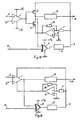
- the first form of the full-wave rectifying circuit includes a comparator stage having a non-inverting input port 6 and an inverting input port 7, a complementary MOS (CMOS) transistor inverter stage including transistors 2 and 3, an exclusive-OR logic stage 4 including a first input port that serves as an input port for the full-wave rectifying circuit and an averaging stage 5 having an output port 9 serving as an output port for the full-wave rectifying circuit.
- CMOS complementary MOS
- the comparator stage 1 has its output port connected to the gate electrodes of the PMOS transistor 2 and the NMOS transistor 3.
- the drain electrodes of the transistors 2 and 3 are connected together and are connected to a second input port of the exclusive-OR logic stage 4.
- the exclusive-OR logic stage 4 has an output port connected to the input port of the averaging stage 5.
- the PMOS transistor 2 and the NMOS transistor 3 are both enhancement mode devices.
- the first form of the full-wave rectifying circuit receives an analogue input signal on the non-inverting input port 6 of the comparator stage 1 and a ramp signal on the inverting input port 7 of the comparator stage 1.
- the comparator stage 1 is energised by an electrical source providing positive (+V 1 ) and negative (-V 1 ) voltages at respective voltage supply ports.
- the input signal applied to the non-inverting input port 6 of the comparator stage 1 may be as represented by the signal A in Fig. 3 of the accompanying drawings and the ramp signal applied to the inverting input port 7 of the comparator stage 1 may be as represented by the signal B in Fig. 3 of the accompanying drawings.
- the ramp signal B consists of linear rising portions joined by abrupt falling portions.
- the signal A is shown as being substantially sinusoidal.
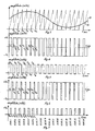
- the comparator stage 1 produces an output signal as shown in Fig. 4 of the accompanying drawings when provided with signals as are shown in Fig. 3 of the accompanying drawings.
- the output signal from the comparator stage 1 is substantially equal to +V 1 volts, the positive supply voltage, when the amplitude of the signal A exceeds the amplitude of the ramp signal B and the output signal of the comparator stage 1 is substantially equal to -V 1 volts, the negative supply voltage, when the amplitude of the signal A is less than the amplitude of the ramp signal B, there being abrupt transitions between the two values of the output signal from the comparator stage 1.
- the output signal from the comparator stage 1 is a width-modulated pulse signal in which the amplitude of the signal A is represented linearly by the widths of the pulses.
- the signal A is recoverable from the output signal from the comparator stage 1 by integration of the output signal from the comparator stage 1 with respect to time. As shown in Fig. 4, the abrupt transitions of the output signal from the comparator 1 occur at times t 1 , t 2 , t 3 ...., and so on, the positive-going transitions occurring at the times t 2 , t 4 ,... and so on.
- the full-wave rectifying circuit shown in Fig. 1 also receives a rectangular clock pulse signal as shown in Fig. 5 of the accompanying drawings, the rectangular clock pulse signal having a 1:1 mark to space ratio and falling edges which coincide with the abrupt falling portions of the ramp signal B.
- the clock signal is applied to the input port B which is the same as the first input port of the exclusive-OR logic stage 4.
- the second input port of the exclusive-OR logic stage 4 receives an inverted form of the output signal from the comparator stage 1 by way of the transistor inverter stage consisting of the transistors 2 and 3. As shown in Fig.
- the rectangular clock pulse signal has abrupt transitions at times t a , t 2 , t b , t 4 , Vietnamese, and so on, the negative-going transitions occurring at the times t 2 , t 4 ,... and so on.
- the signal from the transistor inverter stage 2, 3 is applied to the exclusive-OR logic stage 4 along with the clock pulse signal B and the output signal from the exclusive-OR logic stage 4 is applied to the averaging stage 5 which performs smoothing of the output signal from the full-wave rectifying circuit.
- the signal from the transistor inverter stage 2, 3 is shown in Fig. 6 of the accompanying drawings.
- the signal from the transistor inverter stage 2, 3 is the inverted form of the output signal from the comparator stage 1 shown in Fig. 4 and has limits of +V 3 volts and -V 3 volts set by the supply voltage for the transistors 2, 3.
- the abrupt transitions of the inverted signal provided by the transistor inverter stage 2, 3 still occur at times t 1 , t 2 , t 3 Vietnamese, and so on, but are reversed in relation to the transitions for Fig. 4.
- Fig. 7 of the accompanying drawings shows the output signal from the exclusive-OR logic stage 4 when provided with the signals shown in Figs. 5 and 6 of the accompanying drawings.
- the exclusive-OR logic stage 4 produces an output pulse whenever either one of a clock pulse signal and a width-modulated pulse is present on its own and produces no output pulse for all other relationships between the clock pulse signal and the width-modulated pulse signal.
- the result of the exclusive-OR operation is that the pulse XOR1 extends from t a to t 1 , the pulse XOR2 extends from t b to tt 3 , the pulse XOR3 extends from t c to t 5 , when the clock pulse signal has abrupt transitions at t a , t 2 , t b , t 4 , t c , t 6 , and so on , while the width-modulated pulse signal has abrupt transitions at t 1 , t 2 , t 4 , and so on.
- Fig.7 shows that the pulse XOR1 extends from a time t a to a time t 1 , the pulse XOR2 extends from a time t b to a time t 3 , the pulse XOR3 extends from a time t c to a time t 5 , and so on, where t a , t b and t c are the times at which the clock signal makes its positive transitions and t 1 , t 3 , and t 5 are the times at which the inverted width-modulated pulse signal of Fig. 6 makes its positive transitions.
- the output from the exclusive-OR logic stage 4 of Fig. 1 is unidirectional, as shown in Fig.
- the rectified values XOR1 to XOR9 are substantially the same as the rectified values XOR10 to XOR18 and the accumulated total of the values of the pulses XOR1 to XOR9 is substantially equal to the accumulated total of the values of the pulses XOR10 to XOR18, that expectation being consistent with the estimated totals of the values of those pulses as calculated above.
- the pulses XOR1 to XOR9 relate to a positive half-cycle of the sinusoidal signal A while the pulses XOR10 to XOR18 relate to a negative half-cycle of the sinusoidal signal A and the accumulated total of the values XOR1 to XOR18 represents a full-wave rectified value of the sinusoidal signal A.
- the averaging stage 5 provides a smoothed average value from the pulses XOR1 to XOR18 as an overall output from the full-wave rectifying circuit of Fig. 1.
- the second form of full-wave rectifying circuit includes a comparator stage 1, an exclusive-OR logic stage 4 and an averaging stage 5.
- the second form of full-wave rectifying circuit includes input ports 6,7 and 8 and an output port 9.
- the comparator stage 1 has an output port connected to a first input port of the exclusive-OR logic stage 4 and the input port 8 serves as a second input port of the exclusive-OR logic stage 4.
- the non-inverting and inverting input ports of the comparator stage 1 serve as the input ports 6 and 7 of the full-wave rectifying circuit.
- the exclusive-OR logic stage 4 has an output port connected to the input port of the averaging stage 5.
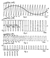
- the second form of full-wave rectifying circuit shown in Fig. 2 is capable of operating with the signals shown in Fig. 8 as input signals, those signals being a substantially sinusoidal signal A and a ramp signal B, the signals A and B represented in Fig. 8 being the same as the signals A and B represented in Fig. 3.
- Fig. 9 shows that the comparator stage 1 provides a width-modulated pulse signal that has abrupt transitions at times t 1 , t 2 , t 3 , and so on, which are the times when the input signal A and the ramp signal B have the same amplitude.
- the width-modulated pulse signal shown in Fig. 9 is positive while the amplitude of the input signal A exceeds that of the ramp signal B and negative when the situation is reversed.
- the maximum and minimum limits of the width-modulated pulse signal of Fig. 9 are +V volts and -V volts, the upper and lower supply voltages to the comparator stage 1.
- Fig. 10 shows a clock pulse signal required for the operation of the full-wave rectifying circuit of Fig. 2, the clock signal being positive initially with negative-going transitions at times t a , t b , t c , and so on, and positive-going transitions at times t 2 , t 4 , t 6 , and so on, where the times t 2 , t 4 , t 6 , and so on, coincide with the abrupt transitions at the times t 2 , t 4 , t 6 , and so on, for the ramp signal B of Fig. 8.
- the clock pulse signal is a rectangular signal having a 1:1 mark to space ratio.
- the width-modulated pulse signal shown in Fig. 9 is the same as the signal shown in Fig. 4 while the clock pulse signal shown in Fig. 10 is the inverted form of the clock pulse signal shown in Fig. 5.
- the exclusive-OR logic stage 4 is driven by the width-modulated pulse signal of Fig. 9 and the clock pulse signal of Fig. 10. As shown in Fig. 11, the exclusive-OR logic stage 4 provides a plurality of positive pulses XOR101, XOR102, XOR103, and so on.
- the pulse XOR101 extends from a time t a to a time t 1
- the pulse XOR102 extends from a time t b to a time t 3
- the pulse XOR103 extends from a time t c to a time t 5 , and so on, from which it can be seen that the pulses XOR101, XOR102, XOR103, and so on, are the same as the pulses XOR1, XOR2, XOR3, and so on, of Fig. 7, establishing that the circuits of Figs. 1 and 2 provide the same result.
- the other relationships established above in respect of Fig. 1 apply to Fig. 2 also.
- the pulse output signal from the exclusive-OR logic stage 4 of Fig. 1 or Fig. 2 may be used as an output signal or may be applied to an averaging stage such as the stage 5 of Fig. 1 or Fig. 2 and that signal used as an output signal.
- the full-wave rectifying circuit of either Fig. 1 or Fig. 2, using the output signal from the averaging stage 5, may be applied to a gain-controlled circuit as shown in either Fig. 12 or Fig. 13 of the accompanying drawings.
- the controlled-gain circuit includes a comparator stage 1, a complementary MOS (CMOS) transistor inverter stage including transistors 2 and 3, an exclusive-OR logic stage 4, an averaging stage 5, an inverting source follower stage including an amplifier 10 with resistors 11 and 12, an output filter stage 13 and an output port 14 connected to the output filter stage 13.
- the comparator stage 1, the CMOS transistor inverter stage including the transistors 2 and 3, the exclusive-OR logic stage 4 and the averaging stage 5 of Fig. 12 are the same as those components of Fig. 1 with the same reference numerals.
- the comparator stage 1 includes non-inverting and inverting input ports 6 and 7.
- the comparator stage 1 has an output port which is connected to to the gate electrodes of the transistors 2 and 3, the transistor 2 being a PMOS enhancement mode device and the transistor 3 being an NMOS enhancement mode device.
- the drain electrodes of the transistors 2 and 3 are connected together and are connected to a first input port of the exclusive-OR logic stage 4.
- the exclusive-OR logic stage 4 has a second input port which serves as an input port 8 of the controlled-gain circuit.
- An output port of the exclusive-OR logic stage 4 is connected to an input port of the averaging stage 5 an output port of which is connected to the source electrode of the PMOS transistor 2.
- the output port of the averaging stage 5 is connected, also, to an input port of the inverting source follower stage which has an output port connected to the source electrode of the NMOS transistor 3.
- An input port of the output filter stage 13 is connected to the drain electrodes of the transistors 2 and 3 while an output port 14 of the output filter stage 13 provides an output port of the controlled-gain circuit.
- the controlled-gain circuit receives an input signal on the non-inverting port 6 of the comparator stage 1 and a ramp signal on the inverting input port 7 of the comparator stage 1.
- the comparator stage 1 is energised by an electrical source providing positive (+V) and negative (-V) voltages at respective voltage supply ports.
- the input signal applied to the non-inverting input port 6 of the comparator stage 1 may be as represented by the signal A and the ramp signal applied to the inverting input port 7 of the comparator stage 1 may be as represented by the signal B, shown in Fig. 14 of the accompanying drawings.
- the ramp signal B consists of linear rising portions joined by abrupt falling portions.
- the signal A is shown as being sinusoidal.
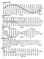
- the comparator stage 1 produces an output signal as shown in Fig. 15 of the accompanying drawings when the signals A and B are applied to its input ports. As shown in Figs. 14 and 15, the output signal from the comparator stage 1 is equal to the positive supply voltage +V 1 volts when the amplitude of the signal A exceeds the amplitude of the ramp signal B and the output signal from the comparator 1 is equal to the negative supply voltage -V 1 volts when the amplitude of the signal A is less than the amplitude of the ramp signal B.
- the transitions between the extremes of the output signal from the comparator stage 1 are abrupt and the output signal is a width-modulated pulse signal in which the widths of the pulses correspond linearly to the amplitudes of the signal A at its intersections with the ramp signal B.
- the signal A is recoverable from the width-modulated pulse signal by integration of the width-modulated pulse signal with respect to time.
- the controlled-gain circuit shown in Fig. 12 also receives a rectangular clock pulse signal as shown in Fig. 17 of the accompanying drawings, the rectangular clock pulse signal having a 1:1 mark to space ratio and falling edges that coincide with the abrupt falling portions of the ramp signal B of Fig. 14.
- the clock pulse signal is applied to the second input port of the exclusive-OR logic stage 4, by way of the input port 8 of the controlled-gain circuit, and the first input port of the exclusive-OR logic stage 4 receives an inverted form of the output signal from the comparator stage 1 as provided by the the transistor inverter stage consisting of the transistors 2 and 3.
- the signal from the transistor inverter stage consisting of the transistors 2 and 3 is applied to the exclusive-OR stage 4 along with the clock pulse signal, the output signal from the exclusive-OR logic stage 4 is applied to the averaging stage 5 and the output signal from the averaging stage 5 is applied to the source electrode of the PMOS transistor 2.
- the output signal from the averaging stage 5 is a positive voltage that is the average of the signal shown in Fig. 18 of the accompanying drawings.
- a negative voltage equal in size to the output signal from the averaging stage 5 is generated by the inverting source follower stage 10, 11, 12 and the negative voltage is applied to the source electrode of the NMOS transistor 3.
- Fig. 16 of the accompanying drawings shows the output signal from the transistor inverter stage consisting of the transistors 2 and 3.
- the source electrode of the PMOS transistor 2 is supplied with the varying voltage provided by the averaging stage 5 and its output signal, being the positive excursions of the signal shown in Fig. 16, varies in amplitude with that supply voltage.
- the source electrode of the NMOS transistor 3 is supplied with a mirror image of the varying voltage from the averaging stage 5 and its output signal is represented by the negative excursions of the signal shown in Fig. 16.
- Comparison of the positive and negative transitions of the signals shown in Figs. 15 and 16 establishes that the signal shown in Fig. 16 is the inverted form of the signal shown in Fig. 15, the signal shown in Fig. 15 being the output signal from the comparator stage 1.
- the estimated integrated values of the signals XOR1 to XOR17 of Fig. 18 from the exclusive-OR logic stage 4 of Fig. 12 are the same as given above for Fig. 7 and the output signal from the averaging circuit 5 is a full-wave rectified value for the input signal A with a scaling factor applied according to the effective gain of the full-wave rectifying part of the circuit of Fig.12.
- the output signal from the averaging stage 5 adjusts gradually from clock pulse to clock pulse and the amplitude variations of the output signal from the transistors 2 and 3 are less rapid than shown in Fig. 16.
- the output filter stage 13 provides a filtered form of the signal shown in Fig. 16 on the output port 14.
- the signal provided on the output port 14 has the form of the input signal A amplified in accordance with the amplitude of the signal A itself.
- Fig. 13 represents a simplified arrangement of the controlled-gain circuit of Fig. 12, the inverting stage formed by the two transistors 2 and 3 being omitted.
- the output port of the averaging stage 5 is connected to the positive voltage supply terminal of the comparator stage 1 and the output port of the inverting source follower stage 10, 11, 12 is connected to the negative voltage supply terminal of the comparator stage 1.
- the output port of the comparator stage 1 is connected to a first input port of the exclusive-OR stage 4 and, also to the input port of the output filter stage 13.
- the simplified controlled-gain circuit shown in Fig. 13 can be regarded as a combination of the full-wave rectifying circuit of Fig. 2 with the source follower stage 10, 11, 12 and the output filter stage 13.
- the operation of the controlled-gain circuit shown in Fig. 13 is understood by considering it as receiving an input signal A and a ramp signal B as shown in Fig. 19, the signals A and B being the same as shown in Figs. 3, 8 and 14.
- the circuit of Fig. 13 requires a clock pulse signal as shown in Fig. 21, that clock pulse signal being the same as the clock pulse signal shown in Fig. 10.
- Fig. 20 shows the output signal from the comparator stage 1 which generates a width-modulated pulse signal with abrupt transitions at the times t 1 , t 2 , t 3 , t 4 , and so on, at which the signals A and B intersect each other, the width-modulated pulse signal being positive when when the input signal A exceeds the ramp signal B in amplitude and negative when the position is reversed.
- the extent to which the width-modulated pulse signal is positive or negative is determined by the supply voltages to the comparator stage 1 and those supply voltages are determined by the output signal from the averaging stage 5.
- the output signal from the averaging stage 5 is applied to the positive supply voltage terminal of the comparator stage 1 while an equal negative voltage, generated by the source follower stage 10, 11 and 12, is applied to the negative supply voltage terminal of the comparator stage 1.
- the overall result is that the comparator stage 1 generates a width-modulated amplitude-modulated signal as shown in Fig. 20 of the accompanying drawings.
- the exclusive-OR logic stage 4 generates a unidirectional pulse signal as shown in Fig. 22, that signal being the same as the signal shown in Figs. 7, 11 and 18.
- the signal shown in Fig. 20 is the inverse of the signal shown in Fig. 16.
- the output filter stage 13 of Fig. 13 provides an output signal at its port 14 that is the same as is provided by the output filter stage 13 of Fig. 12.
- a further alternative arrangement of the controlled-gain circuit of Fig. 12 is obtained by connecting the first input port of the exclusive-OR logic stage 4 to the common gate electrodes of the transistors 2 and 3 instead of to the common drain electrodes of those transistors.
- the further alternative arrangement of the circuit requires the use of the clock pulse signal shown in Fig. 21 and the output signal from the transistors 2 and 3 is as shown in Fig. 16.
- the controlled-gain circuits of Figs. 12 and 13 are nonlinear circuits especially suitable for fabrication using insulated-gate transistors usually referred to as MOS field effect transistors (MOSFETS). Bipolar devices could, nevertheless, be used to fabricate the circuits.
- MOSFETS MOS field effect transistors
- the amplitude-modulated width-modulated signals shown in Figs. 16 and 20 are generated from the input signal A with a controlled amount of non-linearity and an analogue signal is recoverable by filtering each amplitude-modulated width-modulated signal.
- the amount of non-linearity present in the amplitude-modulated width-modulated signals or filtered signals derived from them depends on the gain of the full-wave rectifying part of the controlled-gain circuit used in generating the signals.
Description
- The invention relates to a method and apparatus for processing an analogue signal.
- US-A-4 220 925 discloses an apparatus and method for converting an analogue input signal into a digital signal by modulating the analogue signal with a periodic triangular wave-shape signal to produce intermediate digital signals and performing the exclusive-OR logic function on the intermediate signals with a square wave signal having the same phase as the triangular wave-shape signal.
- US-A-4 059 807 discloses a pulse width modulated amplifier including a mixer including audio and feedback inputs, an integrator for integrating a signal obtained from the mixer, a pulse width modulator responsive to the output signal from the integrator, a filter for filtering the pulse width modulated signal, an output port for applying the filtered signal to a load and a feedback connection to the feedback input of the mixer.
- EP-0 571 289 discloses a circuit for driving a stepping motor. A pulse width-modulated signal is generated from a ROM look up table, which stores half a period of a sine wave; in the pulse width modulated signal the half period of the sine wave is repeated. A square wave having a period equal to that of the sine wave is produced and that is combined with the pulse width modulated signal with an exclusive-OR gate to produce a pulse width modulated signal representing a full sine wave. That signal is, in turn, used to operate switches in a bridge circuit to drive the coils of the motor.
- The present invention provides a method of processing an analogue signal, including the steps of:
- converting the analogue signal into a width-modulated pulse signal by comparing the analogue signal with a ramp signal and generating the width-modulated pulse signal including abrupt transitions occurring at the times when the analogue signal and the ramp signal are of the same amplitude, the ramp signal including abrupt transitions connecting the ramps,
- generating a rectangular clock pulse signal of the same period as the ramp signal and with transitions coincident with the abrupt transitions of the ramp signal and
- generating a resultant signal corresponding to an exclusive-OR combination of the clock pulse signal and the width-modulated pulse signal.
-
- Preferably, an output signal is generated by integrating the resultant signal with respect to time.
- The invention also provides an apparatus for processing an analogue signal including:
- a comparator circuit, for receiving the analogue signal and a ramp signal which includes abrupt transitions connecting the ramps, capable of generating a width-modulated pulse signal including abrupt transitions occurring at the times when the analogue signal and the ramp signal are of the same amplitude and
- an auxiliary circuit, connected to receive the width-modulated pulse signal and a rectangular clock signal of the same period as the ramp signal and with transitions coincident with the abrupt transitions of the ramp signal, capable of generating a resultant signal corresponding to an exclusive-OR combination of the clock pulse signal and the width-modulated pulse signal.
-
- Preferably, the auxiliary circuit includes a logic stage capable of performing the exclusive-OR logic function, the logic stage being connected to receive the clock pulse signal and the width-modulated pulse signal.
- Preferably, an averaging circuit for integrating the resultant signal with respect to time is connected to an output port of the auxiliary circuit.
- The comparator circuit can include a comparator stage driving an inverter stage or the comparator circuit can include the comparator stage alone. In an arrangement including a comparator stage alone, the clock pulse signal required for the support circuit is the inverted form of the clock pulse signal required for the alternative arrangement having a comparator stage driving an inverter stage.
- The analogue signal may be further processed by generating a first output signal by integrating the resultant signal with respect to time and amplitude-modulating the width-modulated pulse signal by means of the first output signal.
- Preferably, a second output signal is generated by integrating the amplitude-modulated width-modulated pulse signal with respect to time.
- An apparatus for further processing the analogue signal includes an averaging stage connected to an output port of the auxiliary circuit for integrating the resultant signal with respect to time and means connecting an output port of the averaging stage to the comparator circuit for amplitude-modulating the width-modulated pulse signal by means of the integrated resultant signal.
- Preferably, the means connecting an output port of the averaging stage to the comparator circuit includes an inverting stage for providing the comparator circuit with a signal of equal and opposite polarity to the integrated resultant signal.
- Preferably, a second averaging stage is included for integrating the amplitude-modulated width-modulated pulse signal with respect to time.
- Apparatus for processing an analogue signal in accordance with the invention will now be described by way of example only, with reference to the accompanying drawings in which:
- Fig. 1 is a diagrammatic representation of a first form of a full-wave rectifying circuit for rectifying an analogue signal,
- Fig. 2 is a diagrammatic representation of a second form of a full-wave rectifying circuit for rectifying an analogue signal,
- Fig. 3 is a diagrammatic representation of an input signal that the full-wave rectifying circuit of Fig. 1 can handle and a ramp signal required to operate the full-wave rectifying circuit of Fig. 1,
- Fig. 4 is a diagrammatic representation of a first width-modulated pulse signal generated within the full-wave rectifying circuit of Fig. 1 when driven by the signals of Fig. 3,
- Fig. 5 is a diagrammatic representation of a clock pulse signal, the first clock pulse signal required by the full-wave rectifying circuit of Fig. 1,
- Fig. 6 is a diagrammatic representation of the inverted form of the first width-modulated pulse signal as generated within the full-wave rectifying circuit of Fig. 1,
- Fig. 7 is a diagrammatic representation of a second width-modulated pulse signal generated as an output signal by the full-wave rectifying circuit of Fig. 1,
- Fig. 8 is a diagrammatic representation of the input and ramp signals of Fig. 3 applied to the second form of full-wave rectifying circuit as represented by Fig. 2,
- Fig. 9 is a diagrammatic representation of a width-modulated pulse signal generated within the second form of full-wave rectifying circuit,
- Fig. 10 is a diagrammatic representation of a clock pulse signal, the second clock pulse signal, required by the secon form of full-wave rectifying circuit, the second clock pulse signal being the inverted form of the first clock pulse signal of Fig. 5,
- Fig. 11 is a diagrammatic representation of a width-modulated pulse signal generated as an output signal by the second form of the full-wave rectifying circuit,
- Fig. 12 is a diagrammatic representation of a first form of controlled-gain circuit for amplifying an analogue signal,
- Fig. 13 is a diagrammatic representation of a second form of controlled-gain circuit for amplifying an analogue signal,
- Fig. 14 is a diagrammatic representation of input and ramp signals for the controlled-gain circuit of Fig. 12,
- Fig. 15 is diagrammatic representation of a width-modulated signal generated within the controlled gain circuit of Fig. 12, when driven by the signals shown in Fig. 14,
- Fig. 16 is a diagrammatic representation of an amplitude-modulated width- modulated pulse signal generated as an output signal by the controlled-gain circuit of Fig. 12 when driven by the signals shown in Fig. 14,
- Fig. 17 is a diagrammatic representation of a clock pulse signal required by the controlled-gain circuit shown in Fig. 12,
- Fig. 18 is a diagrammatic representation of a width-modulated pulse signal generated within the controlled-gain circuit shown in Fig. 12,
- Fig. 19 is a diagrammatic representation of the input and ramp signals of Fig. 14 applied to the second form of controlled-gain circuit shown in Fig. 13,
- Fig. 20 is a diagrammatic representation of an amplitude-modulateed width- modulated signal generated as an output signal by the second form of controlled-gain circuit,
- Fig. 21 is a diagrammatic representation of a clock pulsesignal required by the second form of controlled-gain circuit and
- Fig. 22 is a diagrammatic representation of a width-modulated pulse signal generated within the second form of gain-controlled circuit.
-
- Referring to Fig. 1 of the accompanying drawings, the first form of the full-wave rectifying circuit includes a comparator stage having a non-inverting input port 6 and an inverting input port 7, a complementary MOS (CMOS) transistor inverter
stage including transistors 2 and 3, an exclusive-ORlogic stage 4 including a first input port that serves as an input port for the full-wave rectifying circuit and anaveraging stage 5 having anoutput port 9 serving as an output port for the full-wave rectifying circuit. - The
comparator stage 1 has its output port connected to the gate electrodes of thePMOS transistor 2 and the NMOS transistor 3. The drain electrodes of thetransistors 2 and 3 are connected together and are connected to a second input port of the exclusive-OR logic stage 4. The exclusive-OR logic stage 4 has an output port connected to the input port of theaveraging stage 5. ThePMOS transistor 2 and the NMOS transistor 3 are both enhancement mode devices. - In use, the first form of the full-wave rectifying circuit receives an analogue input signal on the non-inverting input port 6 of the
comparator stage 1 and a ramp signal on the inverting input port 7 of thecomparator stage 1. Thecomparator stage 1 is energised by an electrical source providing positive (+V1) and negative (-V1) voltages at respective voltage supply ports. The input signal applied to the non-inverting input port 6 of thecomparator stage 1 may be as represented by the signal A in Fig. 3 of the accompanying drawings and the ramp signal applied to the inverting input port 7 of thecomparator stage 1 may be as represented by the signal B in Fig. 3 of the accompanying drawings. The ramp signal B consists of linear rising portions joined by abrupt falling portions. The signal A is shown as being substantially sinusoidal. - The
comparator stage 1 produces an output signal as shown in Fig. 4 of the accompanying drawings when provided with signals as are shown in Fig. 3 of the accompanying drawings. As shown in Fig. 4, the output signal from thecomparator stage 1 is substantially equal to +V1 volts, the positive supply voltage, when the amplitude of the signal A exceeds the amplitude of the ramp signal B and the output signal of thecomparator stage 1 is substantially equal to -V1 volts, the negative supply voltage, when the amplitude of the signal A is less than the amplitude of the ramp signal B, there being abrupt transitions between the two values of the output signal from thecomparator stage 1. The output signal from thecomparator stage 1 is a width-modulated pulse signal in which the amplitude of the signal A is represented linearly by the widths of the pulses. The signal A is recoverable from the output signal from thecomparator stage 1 by integration of the output signal from thecomparator stage 1 with respect to time. As shown in Fig. 4, the abrupt transitions of the output signal from thecomparator 1 occur at times t1, t2, t3...., and so on, the positive-going transitions occurring at the times t2, t4,... and so on. - The full-wave rectifying circuit shown in Fig. 1 also receives a rectangular clock pulse signal as shown in Fig. 5 of the accompanying drawings, the rectangular clock pulse signal having a 1:1 mark to space ratio and falling edges which coincide with the abrupt falling portions of the ramp signal B. The clock signal is applied to the input port B which is the same as the first input port of the exclusive-
OR logic stage 4. The second input port of the exclusive-OR logic stage 4 receives an inverted form of the output signal from thecomparator stage 1 by way of the transistor inverter stage consisting of thetransistors 2 and 3. As shown in Fig. 5, the rectangular clock pulse signal has abrupt transitions at times ta, t2, tb, t4,....., and so on, the negative-going transitions occurring at the times t2, t4,... and so on. - The signal from the
transistor inverter stage 2, 3 is applied to the exclusive-OR logic stage 4 along with the clock pulse signal B and the output signal from the exclusive-OR logic stage 4 is applied to the averagingstage 5 which performs smoothing of the output signal from the full-wave rectifying circuit. - The signal from the
transistor inverter stage 2, 3 is shown in Fig. 6 of the accompanying drawings. As shown in Fig. 6, the signal from thetransistor inverter stage 2, 3 is the inverted form of the output signal from thecomparator stage 1 shown in Fig. 4 and has limits of +V3 volts and -V3 volts set by the supply voltage for thetransistors 2, 3. As shown in Fig. 6, the abrupt transitions of the inverted signal provided by thetransistor inverter stage 2, 3 still occur at times t1, t2, t3....., and so on, but are reversed in relation to the transitions for Fig. 4. - Fig. 7 of the accompanying drawings shows the output signal from the exclusive-
OR logic stage 4 when provided with the signals shown in Figs. 5 and 6 of the accompanying drawings. Estimating values of 1.0, 1.5, 2.0, 2.0, 2.5, 2.5, 1.5, 1.0 and 0.5 units of (amplitude x time) for the accumulated values of the signals XOR1 to XOR9 for the first nine clock cycles of the clock signal shown in Fig. 7, the total accumulated value of those nine signals is 14.5 units of (amplitude x time) taking the width of the rectangular clock signal to be 1 unit of time and its amplitude to be 4 units of amplitude. Estimating values of 1.0, 1.5, 2.0, 2.0, 2.5, 2.5, 1.0, 1.5 and 0.5 units of (amplitude x time) for the integrated values of the signals XOR10 to XOR18 for the next nine clock cycles, the total integrated value of those five signals is 14.5 units of (amplitude x time). - The exclusive-
OR logic stage 4 produces an output pulse whenever either one of a clock pulse signal and a width-modulated pulse is present on its own and produces no output pulse for all other relationships between the clock pulse signal and the width-modulated pulse signal. The result of the exclusive-OR operation is that the pulse XOR1 extends from ta to t1, the pulse XOR2 extends from tb to tt3, the pulse XOR3 extends from tc to t5, when the clock pulse signal has abrupt transitions at ta, t2, tb, t4, tc, t6, and so on , while the width-modulated pulse signal has abrupt transitions at t1, t2, t4, and so on. - Fig.7 shows that the pulse XOR1 extends from a time ta to a time t1, the pulse XOR2 extends from a time tb to a time t3, the pulse XOR3 extends from a time tc to a time t5, and so on, where ta, tb and tc are the times at which the clock signal makes its positive transitions and t1, t3, and t5 are the times at which the inverted width-modulated pulse signal of Fig. 6 makes its positive transitions. The output from the exclusive-
OR logic stage 4 of Fig. 1 is unidirectional, as shown in Fig. 7, and provides, in effect, rectified values dependent on the amplitude of the signal A at the times of its intersection with the ramp signal B, the d.c. component of the signal A having been cancelled in thecomparator stage 1 by ensuring that the d.c. level of the ramp signal B is equal to the d.c. level of the signal A. As is evident from the symmetry of the signal A and the ramp signal B about their common d.c. level, the rectified values XOR1 to XOR9 are substantially the same as the rectified values XOR10 to XOR18 and the accumulated total of the values of the pulses XOR1 to XOR9 is substantially equal to the accumulated total of the values of the pulses XOR10 to XOR18, that expectation being consistent with the estimated totals of the values of those pulses as calculated above. The pulses XOR1 to XOR9 relate to a positive half-cycle of the sinusoidal signal A while the pulses XOR10 to XOR18 relate to a negative half-cycle of the sinusoidal signal A and the accumulated total of the values XOR1 to XOR18 represents a full-wave rectified value of the sinusoidal signal A. The averagingstage 5 provides a smoothed average value from the pulses XOR1 to XOR18 as an overall output from the full-wave rectifying circuit of Fig. 1. - Referring to Fig. 2 of the accompanying drawings, the second form of full-wave rectifying circuit includes a
comparator stage 1, an exclusive-OR logic stage 4 and an averagingstage 5. The second form of full-wave rectifying circuit includesinput ports 6,7 and 8 and anoutput port 9. Thecomparator stage 1 has an output port connected to a first input port of the exclusive-OR logic stage 4 and theinput port 8 serves as a second input port of the exclusive-OR logic stage 4. The non-inverting and inverting input ports of thecomparator stage 1 serve as the input ports 6 and 7 of the full-wave rectifying circuit. The exclusive-OR logic stage 4 has an output port connected to the input port of the averagingstage 5. - The second form of full-wave rectifying circuit shown in Fig. 2 is capable of operating with the signals shown in Fig. 8 as input signals, those signals being a substantially sinusoidal signal A and a ramp signal B, the signals A and B represented in Fig. 8 being the same as the signals A and B represented in Fig. 3.
- Fig. 9 shows that the
comparator stage 1 provides a width-modulated pulse signal that has abrupt transitions at times t1, t2, t3, and so on, which are the times when the input signal A and the ramp signal B have the same amplitude. The width-modulated pulse signal shown in Fig. 9 is positive while the amplitude of the input signal A exceeds that of the ramp signal B and negative when the situation is reversed. The maximum and minimum limits of the width-modulated pulse signal of Fig. 9 are +V volts and -V volts, the upper and lower supply voltages to thecomparator stage 1. - Fig. 10 shows a clock pulse signal required for the operation of the full-wave rectifying circuit of Fig. 2, the clock signal being positive initially with negative-going transitions at times ta, tb, tc, and so on, and positive-going transitions at times t2, t4, t6, and so on, where the times t2, t4, t6, and so on, coincide with the abrupt transitions at the times t2, t4, t6, and so on, for the ramp signal B of Fig. 8. The clock pulse signal is a rectangular signal having a 1:1 mark to space ratio.
- The width-modulated pulse signal shown in Fig. 9 is the same as the signal shown in Fig. 4 while the clock pulse signal shown in Fig. 10 is the inverted form of the clock pulse signal shown in Fig. 5.
- The exclusive-
OR logic stage 4 is driven by the width-modulated pulse signal of Fig. 9 and the clock pulse signal of Fig. 10. As shown in Fig. 11, the exclusive-OR logic stage 4 provides a plurality of positive pulses XOR101, XOR102, XOR103, and so on. The pulse XOR101 extends from a time ta to a time t1, the pulse XOR102 extends from a time tb to a time t3, the pulse XOR103 extends from a time tc to a time t5, and so on, from which it can be seen that the pulses XOR101, XOR102, XOR103, and so on, are the same as the pulses XOR1, XOR2, XOR3, and so on, of Fig. 7, establishing that the circuits of Figs. 1 and 2 provide the same result. The other relationships established above in respect of Fig. 1 apply to Fig. 2 also. - The pulse output signal from the exclusive-
OR logic stage 4 of Fig. 1 or Fig. 2 may be used as an output signal or may be applied to an averaging stage such as thestage 5 of Fig. 1 or Fig. 2 and that signal used as an output signal. - The full-wave rectifying circuit of either Fig. 1 or Fig. 2, using the output signal from the averaging
stage 5, may be applied to a gain-controlled circuit as shown in either Fig. 12 or Fig. 13 of the accompanying drawings. - Referring to Fig. 12 of the accompanying drawings, the controlled-gain circuit includes a
comparator stage 1, a complementary MOS (CMOS) transistor inverterstage including transistors 2 and 3, an exclusive-OR logic stage 4, an averagingstage 5, an inverting source follower stage including anamplifier 10 withresistors output filter stage 13 and anoutput port 14 connected to theoutput filter stage 13. Thecomparator stage 1, the CMOS transistor inverter stage including thetransistors 2 and 3, the exclusive-OR logic stage 4 and the averagingstage 5 of Fig. 12 are the same as those components of Fig. 1 with the same reference numerals. - The
comparator stage 1 includes non-inverting and inverting input ports 6 and 7. Thecomparator stage 1 has an output port which is connected to to the gate electrodes of thetransistors 2 and 3, thetransistor 2 being a PMOS enhancement mode device and the transistor 3 being an NMOS enhancement mode device. The drain electrodes of thetransistors 2 and 3 are connected together and are connected to a first input port of the exclusive-OR logic stage 4. The exclusive-OR logic stage 4 has a second input port which serves as aninput port 8 of the controlled-gain circuit. An output port of the exclusive-OR logic stage 4 is connected to an input port of the averagingstage 5 an output port of which is connected to the source electrode of thePMOS transistor 2. The output port of the averagingstage 5 is connected, also, to an input port of the inverting source follower stage which has an output port connected to the source electrode of the NMOS transistor 3. An input port of theoutput filter stage 13 is connected to the drain electrodes of thetransistors 2 and 3 while anoutput port 14 of theoutput filter stage 13 provides an output port of the controlled-gain circuit. - In use, the controlled-gain circuit receives an input signal on the non-inverting port 6 of the
comparator stage 1 and a ramp signal on the inverting input port 7 of thecomparator stage 1. Thecomparator stage 1 is energised by an electrical source providing positive (+V) and negative (-V) voltages at respective voltage supply ports. - The input signal applied to the non-inverting input port 6 of the
comparator stage 1 may be as represented by the signal A and the ramp signal applied to the inverting input port 7 of thecomparator stage 1 may be as represented by the signal B, shown in Fig. 14 of the accompanying drawings. The ramp signal B consists of linear rising portions joined by abrupt falling portions. The signal A is shown as being sinusoidal. - The
comparator stage 1 produces an output signal as shown in Fig. 15 of the accompanying drawings when the signals A and B are applied to its input ports. As shown in Figs. 14 and 15, the output signal from thecomparator stage 1 is equal to the positive supply voltage +V1 volts when the amplitude of the signal A exceeds the amplitude of the ramp signal B and the output signal from thecomparator 1 is equal to the negative supply voltage -V1 volts when the amplitude of the signal A is less than the amplitude of the ramp signal B. The transitions between the extremes of the output signal from thecomparator stage 1 are abrupt and the output signal is a width-modulated pulse signal in which the widths of the pulses correspond linearly to the amplitudes of the signal A at its intersections with the ramp signal B. The signal A is recoverable from the width-modulated pulse signal by integration of the width-modulated pulse signal with respect to time. - The controlled-gain circuit shown in Fig. 12 also receives a rectangular clock pulse signal as shown in Fig. 17 of the accompanying drawings, the rectangular clock pulse signal having a 1:1 mark to space ratio and falling edges that coincide with the abrupt falling portions of the ramp signal B of Fig. 14. The clock pulse signal is applied to the second input port of the exclusive-
OR logic stage 4, by way of theinput port 8 of the controlled-gain circuit, and the first input port of the exclusive-OR logic stage 4 receives an inverted form of the output signal from thecomparator stage 1 as provided by the the transistor inverter stage consisting of thetransistors 2 and 3. - So far, the operation of the controlled-gain circuit of Fig. 12 is the same as that of the circuit of Fig. 1.
- The signal from the transistor inverter stage consisting of the
transistors 2 and 3 is applied to the exclusive-OR stage 4 along with the clock pulse signal, the output signal from the exclusive-OR logic stage 4 is applied to the averagingstage 5 and the output signal from the averagingstage 5 is applied to the source electrode of thePMOS transistor 2. The output signal from the averagingstage 5 is a positive voltage that is the average of the signal shown in Fig. 18 of the accompanying drawings. A negative voltage equal in size to the output signal from the averagingstage 5 is generated by the invertingsource follower stage - It is evident from a comparison of Fig. 18 with Fig. 7 that the output of the exclusive-
OR logic stage 4 is the same for the controlled-gain circuit of Fig. 12 as it is for the rectifying circuit of Fig. 1. - Fig. 16 of the accompanying drawings shows the output signal from the transistor inverter stage consisting of the
transistors 2 and 3. The source electrode of thePMOS transistor 2 is supplied with the varying voltage provided by the averagingstage 5 and its output signal, being the positive excursions of the signal shown in Fig. 16, varies in amplitude with that supply voltage. The source electrode of the NMOS transistor 3 is supplied with a mirror image of the varying voltage from the averagingstage 5 and its output signal is represented by the negative excursions of the signal shown in Fig. 16. Comparison of the positive and negative transitions of the signals shown in Figs. 15 and 16 establishes that the signal shown in Fig. 16 is the inverted form of the signal shown in Fig. 15, the signal shown in Fig. 15 being the output signal from thecomparator stage 1. - The estimated integrated values of the signals XOR1 to XOR17 of Fig. 18 from the exclusive-
OR logic stage 4 of Fig. 12 are the same as given above for Fig. 7 and the output signal from the averagingcircuit 5 is a full-wave rectified value for the input signal A with a scaling factor applied according to the effective gain of the full-wave rectifying part of the circuit of Fig.12. - In practice, the output signal from the averaging
stage 5 adjusts gradually from clock pulse to clock pulse and the amplitude variations of the output signal from thetransistors 2 and 3 are less rapid than shown in Fig. 16. - The
output filter stage 13 provides a filtered form of the signal shown in Fig. 16 on theoutput port 14. - The signal provided on the
output port 14 has the form of the input signal A amplified in accordance with the amplitude of the signal A itself. - Fig. 13 represents a simplified arrangement of the controlled-gain circuit of Fig. 12, the inverting stage formed by the two
transistors 2 and 3 being omitted. - Referring to Fig. 13, the output port of the averaging
stage 5 is connected to the positive voltage supply terminal of thecomparator stage 1 and the output port of the invertingsource follower stage comparator stage 1. The output port of thecomparator stage 1 is connected to a first input port of the exclusive-OR stage 4 and, also to the input port of theoutput filter stage 13. - The simplified controlled-gain circuit shown in Fig. 13 can be regarded as a combination of the full-wave rectifying circuit of Fig. 2 with the
source follower stage output filter stage 13. - The operation of the controlled-gain circuit shown in Fig. 13 is understood by considering it as receiving an input signal A and a ramp signal B as shown in Fig. 19, the signals A and B being the same as shown in Figs. 3, 8 and 14. The circuit of Fig. 13 requires a clock pulse signal as shown in Fig. 21, that clock pulse signal being the same as the clock pulse signal shown in Fig. 10.
- Fig. 20 shows the output signal from the
comparator stage 1 which generates a width-modulated pulse signal with abrupt transitions at the times t1, t2, t3, t4, and so on, at which the signals A and B intersect each other, the width-modulated pulse signal being positive when when the input signal A exceeds the ramp signal B in amplitude and negative when the position is reversed. The extent to which the width-modulated pulse signal is positive or negative is determined by the supply voltages to thecomparator stage 1 and those supply voltages are determined by the output signal from the averagingstage 5. The output signal from the averagingstage 5 is applied to the positive supply voltage terminal of thecomparator stage 1 while an equal negative voltage, generated by thesource follower stage comparator stage 1. The overall result is that thecomparator stage 1 generates a width-modulated amplitude-modulated signal as shown in Fig. 20 of the accompanying drawings. - The exclusive-
OR logic stage 4 generates a unidirectional pulse signal as shown in Fig. 22, that signal being the same as the signal shown in Figs. 7, 11 and 18. - The signal shown in Fig. 20 is the inverse of the signal shown in Fig. 16. The
output filter stage 13 of Fig. 13 provides an output signal at itsport 14 that is the same as is provided by theoutput filter stage 13 of Fig. 12. - A further alternative arrangement of the controlled-gain circuit of Fig. 12 is obtained by connecting the first input port of the exclusive-
OR logic stage 4 to the common gate electrodes of thetransistors 2 and 3 instead of to the common drain electrodes of those transistors. The further alternative arrangement of the circuit requires the use of the clock pulse signal shown in Fig. 21 and the output signal from thetransistors 2 and 3 is as shown in Fig. 16. - The controlled-gain circuits of Figs. 12 and 13 are nonlinear circuits especially suitable for fabrication using insulated-gate transistors usually referred to as MOS field effect transistors (MOSFETS). Bipolar devices could, nevertheless, be used to fabricate the circuits.
- The amplitude-modulated width-modulated signals shown in Figs. 16 and 20 are generated from the input signal A with a controlled amount of non-linearity and an analogue signal is recoverable by filtering each amplitude-modulated width-modulated signal. The amount of non-linearity present in the amplitude-modulated width-modulated signals or filtered signals derived from them depends on the gain of the full-wave rectifying part of the controlled-gain circuit used in generating the signals.
Claims (14)
- A method of processing an analogue signal, including the steps of:converting the analogue signal into a width-modulated pulse signal by comparing the analogue signal with a ramp signal and generating the width-modulated pulse signal including abrupt transitions occurring at the times when the analogue signal and the ramp signal are of the same amplitude, the ramp signal including abrupt transitions connecting the ramps,generating a rectangular clock pulse signal of the same period as the ramp signal and with transitions coincident with the abrupt transitions of the ramp signal andgenerating a resultant signal corresponding to an exclusive-OR combination of the clock pulse signal and the width-modulated pulse signal.
- A method as claimed in claim 1, wherein the rectangular clock pulse signal has a 1:1 mark-to-space ratio.
- A method as claimed in claim 1 or claim 2, wherein an output signal is generated by integrating the resultant signal with respect to time.
- An apparatus for processing an analogue signal including:a comparator circuit, for receiving the analogue signal and a ramp signal which includes abrupt transitions connecting the ramps, capable of generating a width-modulated pulse signal including abrupt transitions occurring at the times when the analogue signal and the ramp signal are of the same amplitude andan auxiliary circuit, connected to receive the width-modulated pulse signal and a rectangular clock signal of the same period as the ramp signal and with transitions coincident with the abrupt transitions of the ramp signal, capable of generating a resultant signal corresponding to an exclusive-OR combination of the clock pulse signal and the width-modulated pulse signal.
- An apparatus as claimed in claim 4, wherein the rectangular clock pulse signal has a 1:1 mark-to-space ratio.
- An apparatus as claimed in claim 4 or claim 5, wherein the auxiliary circuit includes a logic stage capable of performing the exclusive-OR logic function, the logic stage being connected to receive the clock pulse signal and the width-modulated pulse signal.
- An apparatus as claimed in any one of claims 4 to 6, wherein the comparator circuit includes a comparator stage alone.
- An apparatus as claimed in any one of claims 4 to 6, wherein the comparator circuit includes a comparator stage connected to an inverter stage.
- An apparatus as claimed in any one of claims 4 to 8, including an averaging stage connected to an output port of the auxiliary circuit for integrating the resultant signal with respect to time.
- A method of processing an analogue signal as ciaimed in claim 1 or claim 2, including the steps of generating a first output signal by integrating the resultant signal with respect to time and amplitude-modulating he width-modulated pulse signal by means of the first output signal.
- A method as claimed in claim 10, including the step of generating a second output signal by integrating the amplitude-modulated width-modulated pulse signal with respect to time.
- An apparatus as claimed in any one of claims 4 to 8, including an averaging stage connected to an output port of the auxiliary circuit for integrating the resultant signal with respect to time and means connecting an output port of the averaging stage to the comparator circuit for amplitude-modulating the widen-modulated signal by means of the integrated resultant signal.
- An apparatus as claimed in claim 12, wherein the means connecting an output port of the averaging stage to the comparator stage includes an inverting stage for providing, to the comparator circuit, a signal of equal and opposite polarity to the integrated resultant signal.
- An apparatus as claimed in claim 12 or claim 13, including a second averaging stage for integrating the amplitude-modulated width-modulated pulse signal with respect to time.
Applications Claiming Priority (2)
| Application Number | Priority Date | Filing Date | Title |
|---|---|---|---|
| GB9417832 | 1994-09-05 | ||
| GB9417832A GB9417832D0 (en) | 1994-09-05 | 1994-09-05 | A method and apparatus for processing an analogue signal |
Publications (2)
| Publication Number | Publication Date |
|---|---|
| EP0704971A1 EP0704971A1 (en) | 1996-04-03 |
| EP0704971B1 true EP0704971B1 (en) | 2002-07-03 |
Family
ID=10760841
Family Applications (1)
| Application Number | Title | Priority Date | Filing Date |
|---|---|---|---|
| EP95306172A Expired - Lifetime EP0704971B1 (en) | 1994-09-05 | 1995-09-04 | A method and apparatus for processing an analogue signal |
Country Status (5)
| Country | Link |
|---|---|
| US (1) | US5994954A (en) |
| EP (1) | EP0704971B1 (en) |
| JP (1) | JPH08195658A (en) |
| DE (1) | DE69527243T2 (en) |
| GB (1) | GB9417832D0 (en) |
Families Citing this family (1)
| Publication number | Priority date | Publication date | Assignee | Title |
|---|---|---|---|---|
| TW200822537A (en) * | 2006-11-13 | 2008-05-16 | Nanya Technology Corp | Input receiver and related method |
Citations (2)
| Publication number | Priority date | Publication date | Assignee | Title |
|---|---|---|---|---|
| US4059809A (en) * | 1974-08-27 | 1977-11-22 | Siemens Aktiengesellschaft | Differential amplifier |
| EP0571289A1 (en) * | 1992-05-21 | 1993-11-24 | Sony Corporation | Apparatus for driving a stepping motor |
Family Cites Families (8)
| Publication number | Priority date | Publication date | Assignee | Title |
|---|---|---|---|---|
| US3667046A (en) * | 1969-10-09 | 1972-05-30 | Magnavox Co | Voice transmission and receiving system employing pulse duration modulations with a suppressed clock |
| DE2324201A1 (en) * | 1973-05-12 | 1974-11-28 | Launer Hans Gerd Dipl Ing | TRANSMISSION METHOD AND SENDER AND RECEIVER CIRCUIT ARRANGEMENT FOR THE SIMULTANEOUS TRANSMISSION OF TWO SIGNALS USING A TRANSMISSION CHANNEL USING COMBINED PULSE DURATION AND PULSE AMPLITUDE MODULATION |
| US4220925A (en) * | 1977-07-11 | 1980-09-02 | Rca Corporation | Encoding analog signals into digital signals using a triangular reference |
| JPS5922441A (en) * | 1982-07-28 | 1984-02-04 | Hitachi Ltd | Pulse width modulation circuit and digital output type integrating circuit using it |
| FR2558316B1 (en) * | 1984-01-12 | 1989-10-20 | Pophillat Lucien | METHOD FOR SYNCHRONOUSLY MODULATING AN ANALOGUE SIGNAL, MODULATOR AND DEMODULATOR FOR TRANSMITTING A SIGNAL FOLLOWING THIS METHOD AND METHOD FOR TRANSMITTING DIGITAL AND ANALOGUE FRAMED FRAME SIGNALS |
| EP0149577A3 (en) * | 1984-01-16 | 1985-09-11 | Louis Champavier | Method for converting an analog signal into a pulse signal and inverse conversion method, conversion apparatus for implementing these methods, transmission systems and control and regulation systems comprising such apparatus |
| US4673888A (en) * | 1986-09-02 | 1987-06-16 | Electro-Voice, Inc. | Power control system |
| US5428642A (en) * | 1993-11-01 | 1995-06-27 | Ponto; Robert | Power Amplifier |
-
1994
- 1994-09-05 GB GB9417832A patent/GB9417832D0/en active Pending
-
1995
- 1995-09-04 DE DE69527243T patent/DE69527243T2/en not_active Expired - Lifetime
- 1995-09-04 EP EP95306172A patent/EP0704971B1/en not_active Expired - Lifetime
- 1995-09-05 JP JP7263438A patent/JPH08195658A/en active Pending
-
1997
- 1997-03-04 US US08/811,332 patent/US5994954A/en not_active Expired - Lifetime
Patent Citations (2)
| Publication number | Priority date | Publication date | Assignee | Title |
|---|---|---|---|---|
| US4059809A (en) * | 1974-08-27 | 1977-11-22 | Siemens Aktiengesellschaft | Differential amplifier |
| EP0571289A1 (en) * | 1992-05-21 | 1993-11-24 | Sony Corporation | Apparatus for driving a stepping motor |
Also Published As
| Publication number | Publication date |
|---|---|
| JPH08195658A (en) | 1996-07-30 |
| DE69527243T2 (en) | 2003-03-27 |
| EP0704971A1 (en) | 1996-04-03 |
| GB9417832D0 (en) | 1994-10-26 |
| DE69527243D1 (en) | 2002-08-08 |
| US5994954A (en) | 1999-11-30 |
Similar Documents
| Publication | Publication Date | Title |
|---|---|---|
| EP0048786B1 (en) | Variable phase square wave voltage generator | |
| EP0833443B1 (en) | Switching amplifier closed loop dual comparator modulation technique | |
| US6301137B1 (en) | Three-phase current sensor and estimator | |
| JP5042031B2 (en) | Power multiplier apparatus and method | |
| EP0704971B1 (en) | A method and apparatus for processing an analogue signal | |
| CN1292168A (en) | Method in compensation of unlinearities in amplifier, amplifier, and uses of method and amplifier | |
| US4134076A (en) | Pulse width modulated signal amplifier | |
| US4605910A (en) | AM pulse duration modulator | |
| JPH0744403B2 (en) | Low distortion class D power amplifier | |
| JPH0335846B2 (en) | ||
| EP0951146A1 (en) | A digital-to-analog converter | |
| SU964969A1 (en) | Pulse-width amplifier | |
| JP2689712B2 (en) | PWM conversion circuit | |
| US6703886B2 (en) | Circuit arrangement for rectifying a signal | |
| JPH0354481B2 (en) | ||
| JP2861154B2 (en) | AGC and ADC adjustment method for A / D converter input signal | |
| JPS62109424A (en) | Output circuit for pulse modulator | |
| JPH0520007Y2 (en) | ||
| JPS6145900B2 (en) | ||
| US4626790A (en) | Demodulator for amplitude-modulated carrier frequency oscillations | |
| JPH0546723B2 (en) | ||
| JPS60169205A (en) | High efficient switch amplifier | |
| JPH062836U (en) | Digital-to-analog converter | |
| JPH0380363B2 (en) | ||
| JPH0622540A (en) | Switching power supply |
Legal Events
| Date | Code | Title | Description |
|---|---|---|---|
| PUAI | Public reference made under article 153(3) epc to a published international application that has entered the european phase |
Free format text: ORIGINAL CODE: 0009012 |
|
| AK | Designated contracting states |
Kind code of ref document: A1 Designated state(s): DE FR GB IT NL |
|
| 17P | Request for examination filed |
Effective date: 19961003 |
|
| 17Q | First examination report despatched |
Effective date: 19990707 |
|
| GRAG | Despatch of communication of intention to grant |
Free format text: ORIGINAL CODE: EPIDOS AGRA |
|
| GRAG | Despatch of communication of intention to grant |
Free format text: ORIGINAL CODE: EPIDOS AGRA |
|
| GRAH | Despatch of communication of intention to grant a patent |
Free format text: ORIGINAL CODE: EPIDOS IGRA |
|
| GRAH | Despatch of communication of intention to grant a patent |
Free format text: ORIGINAL CODE: EPIDOS IGRA |
|
| GRAA | (expected) grant |
Free format text: ORIGINAL CODE: 0009210 |
|
| AK | Designated contracting states |
Kind code of ref document: B1 Designated state(s): DE FR GB IT NL |
|
| PG25 | Lapsed in a contracting state [announced via postgrant information from national office to epo] |
Ref country code: NL Free format text: LAPSE BECAUSE OF FAILURE TO SUBMIT A TRANSLATION OF THE DESCRIPTION OR TO PAY THE FEE WITHIN THE PRESCRIBED TIME-LIMIT Effective date: 20020703 Ref country code: IT Free format text: LAPSE BECAUSE OF FAILURE TO SUBMIT A TRANSLATION OF THE DESCRIPTION OR TO PAY THE FEE WITHIN THE PRE;WARNING: LAPSES OF ITALIAN PATENTS WITH EFFECTIVE DATE BEFORE 2007 MAY HAVE OCCURRED AT ANY TIME BEFORE 2007. THE CORRECT EFFECTIVE DATE MAY BE DIFFERENT FROM THE ONE RECORDED.SCRIBED TIME-LIMIT Effective date: 20020703 |
|
| REF | Corresponds to: |
Ref document number: 69527243 Country of ref document: DE Date of ref document: 20020808 |
|
| NLV1 | Nl: lapsed or annulled due to failure to fulfill the requirements of art. 29p and 29m of the patents act | ||
| ET | Fr: translation filed | ||
| PLBE | No opposition filed within time limit |
Free format text: ORIGINAL CODE: 0009261 |
|
| STAA | Information on the status of an ep patent application or granted ep patent |
Free format text: STATUS: NO OPPOSITION FILED WITHIN TIME LIMIT |
|
| 26N | No opposition filed |
Effective date: 20030404 |
|
| PGFP | Annual fee paid to national office [announced via postgrant information from national office to epo] |
Ref country code: GB Payment date: 20100809 Year of fee payment: 16 |
|
| PGFP | Annual fee paid to national office [announced via postgrant information from national office to epo] |
Ref country code: DE Payment date: 20100930 Year of fee payment: 16 |
|
| REG | Reference to a national code |
Ref country code: FR Ref legal event code: ST Effective date: 20110531 |
|
| PG25 | Lapsed in a contracting state [announced via postgrant information from national office to epo] |
Ref country code: FR Free format text: LAPSE BECAUSE OF NON-PAYMENT OF DUE FEES Effective date: 20100930 |
|
| PGFP | Annual fee paid to national office [announced via postgrant information from national office to epo] |
Ref country code: FR Payment date: 20090916 Year of fee payment: 15 |
|
| GBPC | Gb: european patent ceased through non-payment of renewal fee |
Effective date: 20110904 |
|
| REG | Reference to a national code |
Ref country code: DE Ref legal event code: R119 Ref document number: 69527243 Country of ref document: DE Effective date: 20120403 |
|
| PG25 | Lapsed in a contracting state [announced via postgrant information from national office to epo] |
Ref country code: DE Free format text: LAPSE BECAUSE OF NON-PAYMENT OF DUE FEES Effective date: 20120403 |
|
| PG25 | Lapsed in a contracting state [announced via postgrant information from national office to epo] |
Ref country code: GB Free format text: LAPSE BECAUSE OF NON-PAYMENT OF DUE FEES Effective date: 20110904 |