EP0704897B1 - Semiconductor device with metal plate - Google Patents
Semiconductor device with metal plate Download PDFInfo
- Publication number
- EP0704897B1 EP0704897B1 EP95306885A EP95306885A EP0704897B1 EP 0704897 B1 EP0704897 B1 EP 0704897B1 EP 95306885 A EP95306885 A EP 95306885A EP 95306885 A EP95306885 A EP 95306885A EP 0704897 B1 EP0704897 B1 EP 0704897B1
- Authority
- EP
- European Patent Office
- Prior art keywords
- bumps
- base film
- film sheet
- via holes
- semiconductor device
- Prior art date
- Legal status (The legal status is an assumption and is not a legal conclusion. Google has not performed a legal analysis and makes no representation as to the accuracy of the status listed.)
- Expired - Lifetime
Links
Images


Classifications
-
- H—ELECTRICITY
- H01—ELECTRIC ELEMENTS
- H01L—SEMICONDUCTOR DEVICES NOT COVERED BY CLASS H10
- H01L24/00—Arrangements for connecting or disconnecting semiconductor or solid-state bodies; Methods or apparatus related thereto
- H01L24/01—Means for bonding being attached to, or being formed on, the surface to be connected, e.g. chip-to-package, die-attach, "first-level" interconnects; Manufacturing methods related thereto
- H01L24/50—Tape automated bonding [TAB] connectors, i.e. film carriers; Manufacturing methods related thereto
-
- H—ELECTRICITY
- H01—ELECTRIC ELEMENTS
- H01L—SEMICONDUCTOR DEVICES NOT COVERED BY CLASS H10
- H01L23/00—Details of semiconductor or other solid state devices
- H01L23/28—Encapsulations, e.g. encapsulating layers, coatings, e.g. for protection
- H01L23/31—Encapsulations, e.g. encapsulating layers, coatings, e.g. for protection characterised by the arrangement or shape
- H01L23/3107—Encapsulations, e.g. encapsulating layers, coatings, e.g. for protection characterised by the arrangement or shape the device being completely enclosed
-
- H—ELECTRICITY
- H01—ELECTRIC ELEMENTS
- H01L—SEMICONDUCTOR DEVICES NOT COVERED BY CLASS H10
- H01L23/00—Details of semiconductor or other solid state devices
- H01L23/48—Arrangements for conducting electric current to or from the solid state body in operation, e.g. leads, terminal arrangements ; Selection of materials therefor
- H01L23/488—Arrangements for conducting electric current to or from the solid state body in operation, e.g. leads, terminal arrangements ; Selection of materials therefor consisting of soldered or bonded constructions
- H01L23/495—Lead-frames or other flat leads
- H01L23/49572—Lead-frames or other flat leads consisting of thin flexible metallic tape with or without a film carrier
-
- H—ELECTRICITY
- H01—ELECTRIC ELEMENTS
- H01L—SEMICONDUCTOR DEVICES NOT COVERED BY CLASS H10
- H01L23/00—Details of semiconductor or other solid state devices
- H01L23/48—Arrangements for conducting electric current to or from the solid state body in operation, e.g. leads, terminal arrangements ; Selection of materials therefor
- H01L23/488—Arrangements for conducting electric current to or from the solid state body in operation, e.g. leads, terminal arrangements ; Selection of materials therefor consisting of soldered or bonded constructions
- H01L23/498—Leads, i.e. metallisations or lead-frames on insulating substrates, e.g. chip carriers
- H01L23/49811—Additional leads joined to the metallisation on the insulating substrate, e.g. pins, bumps, wires, flat leads
- H01L23/49816—Spherical bumps on the substrate for external connection, e.g. ball grid arrays [BGA]
-
- H—ELECTRICITY
- H01—ELECTRIC ELEMENTS
- H01L—SEMICONDUCTOR DEVICES NOT COVERED BY CLASS H10
- H01L23/00—Details of semiconductor or other solid state devices
- H01L23/48—Arrangements for conducting electric current to or from the solid state body in operation, e.g. leads, terminal arrangements ; Selection of materials therefor
- H01L23/488—Arrangements for conducting electric current to or from the solid state body in operation, e.g. leads, terminal arrangements ; Selection of materials therefor consisting of soldered or bonded constructions
- H01L23/498—Leads, i.e. metallisations or lead-frames on insulating substrates, e.g. chip carriers
- H01L23/49833—Leads, i.e. metallisations or lead-frames on insulating substrates, e.g. chip carriers the chip support structure consisting of a plurality of insulating substrates
-
- H—ELECTRICITY
- H01—ELECTRIC ELEMENTS
- H01L—SEMICONDUCTOR DEVICES NOT COVERED BY CLASS H10
- H01L23/00—Details of semiconductor or other solid state devices
- H01L23/48—Arrangements for conducting electric current to or from the solid state body in operation, e.g. leads, terminal arrangements ; Selection of materials therefor
- H01L23/488—Arrangements for conducting electric current to or from the solid state body in operation, e.g. leads, terminal arrangements ; Selection of materials therefor consisting of soldered or bonded constructions
- H01L23/498—Leads, i.e. metallisations or lead-frames on insulating substrates, e.g. chip carriers
- H01L23/49838—Geometry or layout
-
- H—ELECTRICITY
- H01—ELECTRIC ELEMENTS
- H01L—SEMICONDUCTOR DEVICES NOT COVERED BY CLASS H10
- H01L25/00—Assemblies consisting of a plurality of individual semiconductor or other solid state devices ; Multistep manufacturing processes thereof
- H01L25/03—Assemblies consisting of a plurality of individual semiconductor or other solid state devices ; Multistep manufacturing processes thereof all the devices being of a type provided for in the same subgroup of groups H01L27/00 - H01L33/00, or in a single subclass of H10K, H10N, e.g. assemblies of rectifier diodes
- H01L25/10—Assemblies consisting of a plurality of individual semiconductor or other solid state devices ; Multistep manufacturing processes thereof all the devices being of a type provided for in the same subgroup of groups H01L27/00 - H01L33/00, or in a single subclass of H10K, H10N, e.g. assemblies of rectifier diodes the devices having separate containers
- H01L25/105—Assemblies consisting of a plurality of individual semiconductor or other solid state devices ; Multistep manufacturing processes thereof all the devices being of a type provided for in the same subgroup of groups H01L27/00 - H01L33/00, or in a single subclass of H10K, H10N, e.g. assemblies of rectifier diodes the devices having separate containers the devices being of a type provided for in group H01L27/00
-
- H—ELECTRICITY
- H01—ELECTRIC ELEMENTS
- H01L—SEMICONDUCTOR DEVICES NOT COVERED BY CLASS H10
- H01L2224/00—Indexing scheme for arrangements for connecting or disconnecting semiconductor or solid-state bodies and methods related thereto as covered by H01L24/00
- H01L2224/01—Means for bonding being attached to, or being formed on, the surface to be connected, e.g. chip-to-package, die-attach, "first-level" interconnects; Manufacturing methods related thereto
- H01L2224/26—Layer connectors, e.g. plate connectors, solder or adhesive layers; Manufacturing methods related thereto
- H01L2224/31—Structure, shape, material or disposition of the layer connectors after the connecting process
- H01L2224/32—Structure, shape, material or disposition of the layer connectors after the connecting process of an individual layer connector
- H01L2224/321—Disposition
- H01L2224/32151—Disposition the layer connector connecting between a semiconductor or solid-state body and an item not being a semiconductor or solid-state body, e.g. chip-to-substrate, chip-to-passive
- H01L2224/32221—Disposition the layer connector connecting between a semiconductor or solid-state body and an item not being a semiconductor or solid-state body, e.g. chip-to-substrate, chip-to-passive the body and the item being stacked
- H01L2224/32225—Disposition the layer connector connecting between a semiconductor or solid-state body and an item not being a semiconductor or solid-state body, e.g. chip-to-substrate, chip-to-passive the body and the item being stacked the item being non-metallic, e.g. insulating substrate with or without metallisation
-
- H—ELECTRICITY
- H01—ELECTRIC ELEMENTS
- H01L—SEMICONDUCTOR DEVICES NOT COVERED BY CLASS H10
- H01L2225/00—Details relating to assemblies covered by the group H01L25/00 but not provided for in its subgroups
- H01L2225/03—All the devices being of a type provided for in the same subgroup of groups H01L27/00 - H01L33/648 and H10K99/00
- H01L2225/10—All the devices being of a type provided for in the same subgroup of groups H01L27/00 - H01L33/648 and H10K99/00 the devices having separate containers
- H01L2225/1005—All the devices being of a type provided for in the same subgroup of groups H01L27/00 - H01L33/648 and H10K99/00 the devices having separate containers the devices being of a type provided for in group H01L27/00
- H01L2225/1011—All the devices being of a type provided for in the same subgroup of groups H01L27/00 - H01L33/648 and H10K99/00 the devices having separate containers the devices being of a type provided for in group H01L27/00 the containers being in a stacked arrangement
- H01L2225/1017—All the devices being of a type provided for in the same subgroup of groups H01L27/00 - H01L33/648 and H10K99/00 the devices having separate containers the devices being of a type provided for in group H01L27/00 the containers being in a stacked arrangement the lowermost container comprising a device support
- H01L2225/1035—All the devices being of a type provided for in the same subgroup of groups H01L27/00 - H01L33/648 and H10K99/00 the devices having separate containers the devices being of a type provided for in group H01L27/00 the containers being in a stacked arrangement the lowermost container comprising a device support the device being entirely enclosed by the support, e.g. high-density interconnect [HDI]
-
- H—ELECTRICITY
- H01—ELECTRIC ELEMENTS
- H01L—SEMICONDUCTOR DEVICES NOT COVERED BY CLASS H10
- H01L2225/00—Details relating to assemblies covered by the group H01L25/00 but not provided for in its subgroups
- H01L2225/03—All the devices being of a type provided for in the same subgroup of groups H01L27/00 - H01L33/648 and H10K99/00
- H01L2225/10—All the devices being of a type provided for in the same subgroup of groups H01L27/00 - H01L33/648 and H10K99/00 the devices having separate containers
- H01L2225/1005—All the devices being of a type provided for in the same subgroup of groups H01L27/00 - H01L33/648 and H10K99/00 the devices having separate containers the devices being of a type provided for in group H01L27/00
- H01L2225/1011—All the devices being of a type provided for in the same subgroup of groups H01L27/00 - H01L33/648 and H10K99/00 the devices having separate containers the devices being of a type provided for in group H01L27/00 the containers being in a stacked arrangement
- H01L2225/1047—Details of electrical connections between containers
- H01L2225/1058—Bump or bump-like electrical connections, e.g. balls, pillars, posts
-
- H—ELECTRICITY
- H01—ELECTRIC ELEMENTS
- H01L—SEMICONDUCTOR DEVICES NOT COVERED BY CLASS H10
- H01L2225/00—Details relating to assemblies covered by the group H01L25/00 but not provided for in its subgroups
- H01L2225/03—All the devices being of a type provided for in the same subgroup of groups H01L27/00 - H01L33/648 and H10K99/00
- H01L2225/10—All the devices being of a type provided for in the same subgroup of groups H01L27/00 - H01L33/648 and H10K99/00 the devices having separate containers
- H01L2225/1005—All the devices being of a type provided for in the same subgroup of groups H01L27/00 - H01L33/648 and H10K99/00 the devices having separate containers the devices being of a type provided for in group H01L27/00
- H01L2225/1011—All the devices being of a type provided for in the same subgroup of groups H01L27/00 - H01L33/648 and H10K99/00 the devices having separate containers the devices being of a type provided for in group H01L27/00 the containers being in a stacked arrangement
- H01L2225/1094—Thermal management, e.g. cooling
-
- H—ELECTRICITY
- H01—ELECTRIC ELEMENTS
- H01L—SEMICONDUCTOR DEVICES NOT COVERED BY CLASS H10
- H01L24/00—Arrangements for connecting or disconnecting semiconductor or solid-state bodies; Methods or apparatus related thereto
- H01L24/80—Methods for connecting semiconductor or other solid state bodies using means for bonding being attached to, or being formed on, the surface to be connected
- H01L24/86—Methods for connecting semiconductor or other solid state bodies using means for bonding being attached to, or being formed on, the surface to be connected using tape automated bonding [TAB]
-
- H—ELECTRICITY
- H01—ELECTRIC ELEMENTS
- H01L—SEMICONDUCTOR DEVICES NOT COVERED BY CLASS H10
- H01L2924/00—Indexing scheme for arrangements or methods for connecting or disconnecting semiconductor or solid-state bodies as covered by H01L24/00
- H01L2924/01—Chemical elements
- H01L2924/01005—Boron [B]
-
- H—ELECTRICITY
- H01—ELECTRIC ELEMENTS
- H01L—SEMICONDUCTOR DEVICES NOT COVERED BY CLASS H10
- H01L2924/00—Indexing scheme for arrangements or methods for connecting or disconnecting semiconductor or solid-state bodies as covered by H01L24/00
- H01L2924/01—Chemical elements
- H01L2924/01006—Carbon [C]
-
- H—ELECTRICITY
- H01—ELECTRIC ELEMENTS
- H01L—SEMICONDUCTOR DEVICES NOT COVERED BY CLASS H10
- H01L2924/00—Indexing scheme for arrangements or methods for connecting or disconnecting semiconductor or solid-state bodies as covered by H01L24/00
- H01L2924/01—Chemical elements
- H01L2924/01033—Arsenic [As]
-
- H—ELECTRICITY
- H01—ELECTRIC ELEMENTS
- H01L—SEMICONDUCTOR DEVICES NOT COVERED BY CLASS H10
- H01L2924/00—Indexing scheme for arrangements or methods for connecting or disconnecting semiconductor or solid-state bodies as covered by H01L24/00
- H01L2924/01—Chemical elements
- H01L2924/01047—Silver [Ag]
-
- H—ELECTRICITY
- H01—ELECTRIC ELEMENTS
- H01L—SEMICONDUCTOR DEVICES NOT COVERED BY CLASS H10
- H01L2924/00—Indexing scheme for arrangements or methods for connecting or disconnecting semiconductor or solid-state bodies as covered by H01L24/00
- H01L2924/01—Chemical elements
- H01L2924/01074—Tungsten [W]
-
- H—ELECTRICITY
- H01—ELECTRIC ELEMENTS
- H01L—SEMICONDUCTOR DEVICES NOT COVERED BY CLASS H10
- H01L2924/00—Indexing scheme for arrangements or methods for connecting or disconnecting semiconductor or solid-state bodies as covered by H01L24/00
- H01L2924/01—Chemical elements
- H01L2924/01082—Lead [Pb]
-
- H—ELECTRICITY
- H01—ELECTRIC ELEMENTS
- H01L—SEMICONDUCTOR DEVICES NOT COVERED BY CLASS H10
- H01L2924/00—Indexing scheme for arrangements or methods for connecting or disconnecting semiconductor or solid-state bodies as covered by H01L24/00
- H01L2924/095—Indexing scheme for arrangements or methods for connecting or disconnecting semiconductor or solid-state bodies as covered by H01L24/00 with a principal constituent of the material being a combination of two or more materials provided in the groups H01L2924/013 - H01L2924/0715
- H01L2924/097—Glass-ceramics, e.g. devitrified glass
- H01L2924/09701—Low temperature co-fired ceramic [LTCC]
-
- H—ELECTRICITY
- H01—ELECTRIC ELEMENTS
- H01L—SEMICONDUCTOR DEVICES NOT COVERED BY CLASS H10
- H01L2924/00—Indexing scheme for arrangements or methods for connecting or disconnecting semiconductor or solid-state bodies as covered by H01L24/00
- H01L2924/15—Details of package parts other than the semiconductor or other solid state devices to be connected
- H01L2924/151—Die mounting substrate
- H01L2924/1515—Shape
- H01L2924/15153—Shape the die mounting substrate comprising a recess for hosting the device
-
- H—ELECTRICITY
- H01—ELECTRIC ELEMENTS
- H01L—SEMICONDUCTOR DEVICES NOT COVERED BY CLASS H10
- H01L2924/00—Indexing scheme for arrangements or methods for connecting or disconnecting semiconductor or solid-state bodies as covered by H01L24/00
- H01L2924/15—Details of package parts other than the semiconductor or other solid state devices to be connected
- H01L2924/151—Die mounting substrate
- H01L2924/15165—Monolayer substrate
-
- H—ELECTRICITY
- H01—ELECTRIC ELEMENTS
- H01L—SEMICONDUCTOR DEVICES NOT COVERED BY CLASS H10
- H01L2924/00—Indexing scheme for arrangements or methods for connecting or disconnecting semiconductor or solid-state bodies as covered by H01L24/00
- H01L2924/15—Details of package parts other than the semiconductor or other solid state devices to be connected
- H01L2924/151—Die mounting substrate
- H01L2924/153—Connection portion
- H01L2924/1531—Connection portion the connection portion being formed only on the surface of the substrate opposite to the die mounting surface
- H01L2924/15311—Connection portion the connection portion being formed only on the surface of the substrate opposite to the die mounting surface being a ball array, e.g. BGA
-
- H—ELECTRICITY
- H01—ELECTRIC ELEMENTS
- H01L—SEMICONDUCTOR DEVICES NOT COVERED BY CLASS H10
- H01L2924/00—Indexing scheme for arrangements or methods for connecting or disconnecting semiconductor or solid-state bodies as covered by H01L24/00
- H01L2924/15—Details of package parts other than the semiconductor or other solid state devices to be connected
- H01L2924/151—Die mounting substrate
- H01L2924/153—Connection portion
- H01L2924/1532—Connection portion the connection portion being formed on the die mounting surface of the substrate
- H01L2924/1533—Connection portion the connection portion being formed on the die mounting surface of the substrate the connection portion being formed both on the die mounting surface of the substrate and outside the die mounting surface of the substrate
- H01L2924/15331—Connection portion the connection portion being formed on the die mounting surface of the substrate the connection portion being formed both on the die mounting surface of the substrate and outside the die mounting surface of the substrate being a ball array, e.g. BGA
-
- H—ELECTRICITY
- H01—ELECTRIC ELEMENTS
- H01L—SEMICONDUCTOR DEVICES NOT COVERED BY CLASS H10
- H01L2924/00—Indexing scheme for arrangements or methods for connecting or disconnecting semiconductor or solid-state bodies as covered by H01L24/00
- H01L2924/30—Technical effects
- H01L2924/301—Electrical effects
- H01L2924/3025—Electromagnetic shielding
-
- H—ELECTRICITY
- H01—ELECTRIC ELEMENTS
- H01L—SEMICONDUCTOR DEVICES NOT COVERED BY CLASS H10
- H01L2924/00—Indexing scheme for arrangements or methods for connecting or disconnecting semiconductor or solid-state bodies as covered by H01L24/00
- H01L2924/30—Technical effects
- H01L2924/35—Mechanical effects
- H01L2924/351—Thermal stress
- H01L2924/3511—Warping
-
- H—ELECTRICITY
- H05—ELECTRIC TECHNIQUES NOT OTHERWISE PROVIDED FOR
- H05K—PRINTED CIRCUITS; CASINGS OR CONSTRUCTIONAL DETAILS OF ELECTRIC APPARATUS; MANUFACTURE OF ASSEMBLAGES OF ELECTRICAL COMPONENTS
- H05K1/00—Printed circuits
- H05K1/02—Details
- H05K1/14—Structural association of two or more printed circuits
- H05K1/141—One or more single auxiliary printed circuits mounted on a main printed circuit, e.g. modules, adapters
-
- H—ELECTRICITY
- H05—ELECTRIC TECHNIQUES NOT OTHERWISE PROVIDED FOR
- H05K—PRINTED CIRCUITS; CASINGS OR CONSTRUCTIONAL DETAILS OF ELECTRIC APPARATUS; MANUFACTURE OF ASSEMBLAGES OF ELECTRICAL COMPONENTS
- H05K3/00—Apparatus or processes for manufacturing printed circuits
- H05K3/30—Assembling printed circuits with electric components, e.g. with resistor
- H05K3/32—Assembling printed circuits with electric components, e.g. with resistor electrically connecting electric components or wires to printed circuits
- H05K3/34—Assembling printed circuits with electric components, e.g. with resistor electrically connecting electric components or wires to printed circuits by soldering
- H05K3/341—Surface mounted components
- H05K3/3431—Leadless components
-
- H—ELECTRICITY
- H05—ELECTRIC TECHNIQUES NOT OTHERWISE PROVIDED FOR
- H05K—PRINTED CIRCUITS; CASINGS OR CONSTRUCTIONAL DETAILS OF ELECTRIC APPARATUS; MANUFACTURE OF ASSEMBLAGES OF ELECTRICAL COMPONENTS
- H05K3/00—Apparatus or processes for manufacturing printed circuits
- H05K3/36—Assembling printed circuits with other printed circuits
- H05K3/368—Assembling printed circuits with other printed circuits parallel to each other
Landscapes
- Engineering & Computer Science (AREA)
- Microelectronics & Electronic Packaging (AREA)
- Power Engineering (AREA)
- Physics & Mathematics (AREA)
- Computer Hardware Design (AREA)
- Condensed Matter Physics & Semiconductors (AREA)
- General Physics & Mathematics (AREA)
- Geometry (AREA)
- Wire Bonding (AREA)
- Internal Circuitry In Semiconductor Integrated Circuit Devices (AREA)
Description
- This invention relates to a semiconductor device which has a semiconductor chip mounted on a base film.
- Heretofore, a semiconductor device of the type described has been proposed in Japanese Patent Application No. Hei 6-94881, namely, 94881/1994 (JP-A-8 031 869). Specifically, the semiconductor device includes an insulator film which may be called a base film and which has a center region and a peripheral region surrounding the center region. A semiconductor chip which has a great number of elements and a plurality of chip electrodes is located within an opening or a device hole formed in the center region and is resin-molded while a plurality of conductive pads are laid on the peripheral region and are electrically connected to the chip electrodes through inner leads. To the conductive pads, solder bumps are attached as outer connection electrode members and are projected from a surface of the base film.
- With this structure, the solder bumps on the base film can be directly mounted onto a circuit board, such as a mother board with the solder bumps faced with the circuit board. Therefore, the base film substantially serves as a package member. Since the inner leads are laid only within the base film, the semiconductor device is small in size.
- Moreover, the semiconductor device mentioned above is inexpensive in comparison with a semiconductor device which has a ceramic package, because the base film is much cheaper than the ceramic package.
- Herein, it is to be noted that a front surface of the semiconductor chip is directed towards the circuit board while a back surface of the semiconductor chip is exposed to an atmosphere when the solder bumps are mounted on the circuit board. Therefore, the semiconductor device is disadvantageous in that the semiconductor chip is liable to be contaminated or polluted and that the elements in the semiconductor chip can not be electromagnetically shielded.
- Furthermore, the elements in the semiconductor device are formed on a side of the front surface to which the solder bumps are attached. Thus, the elements are faced with the circuit board with gaps which are defined by the solder bumps and which are left between the elements and the circuit board. This structure is not enough to radiate heat from the elements included in the semiconductor device.
- In addition, the semiconductor device should be electrically tested by the use of a probe after it is mounted on the circuit board, so as to check whether or not the elements are normal. However, the above-mentioned semiconductor device can not be checked after it is mounted on the circuit board.
- JP-A-56 134743 describes an arrangement for mounting a semiconductor chip on a flexible insulating film, the latter including inner leads projecting around a chip hole. An arrangement of through-pins is provided for stacking a number of such devices.
- US-A- 5 045 921 describes a pad array carrier IC device using flexible tape, the latter having through-holes which are filled with conductive material in electrical contact with an array of bumps.
- US-A- 5 045 914 describes a resin-moulded IC package having a metal plate electrically connected to the lead frame.
- US-A-5 291 062 describes an area array IC device having a lid with functional contacts.
- It is an object of at least the preferred embodiments of this invention to provide a semiconductor device which can avoid contamination of elements after mounting the semiconductor device on a circuit board.
- It is another such object to provide a semiconductor device of the type described, which can effectively radiate heat from the elements.
- It is still another such object to provide a semiconductor device of the type described, which is capable of readily checking the elements after mounting the semiconductor device on the circuit board.
- In a first aspect, the present invention provides a semiconductor device, comprising:
- a base film sheet which has a center region, a device hole in said center region, a peripheral region surrounding said center region, and a plurality of via holes bored on the peripheral region;
- a semiconductor chip attached to said base film sheet in said device hole of said center region;
- an electric connection member which is laid on said peripheral region and electrically connected to said semiconductor chip, said electric connection member comprising a plurality of lands arranged on said peripheral portion of said base film sheet and located at the position of said plurality of said via holes, and a plurality of inner leads connected to said lands and said semiconductor chip;
- an outer electrode member which has a portion positioned at said plurality of via holes and which is electrically connected to said electric connection member, said outer electrode member comprising a plurality of first bumps mounted on said lands and projecting from said base film sheet; and
- a metal plate member electrically connected to said first bumps through said plurality of via holes, said metal plate member comprising a plate surface and a plurality of second bumps attached to said plate surface facing said via holes of said base film sheet and electrically connected to said first bumps through said via holes, said metal plate having a center area, a peripheral area which surrounds said center area on said plate surface, and a hole formed on said center area and covering the peripheral region of said base film sheet with said semiconductor chip left uncovered, said second bumps being formed on said peripheral area and projecting towards said base film sheet.
-
- In a second aspect, the present invention provides a semiconductor device, comprising:
- a base film sheet which has a center region, a device hole in said center region, a peripheral region surrounding said center region, and a plurality of via holes bored on the peripheral region;
- a semiconductor chip attached to said base film sheet in said device hole of said center region;
- an electric connection member which is laid on said peripheral region and electrically connected to said semiconductor chip, said electric connection member comprising a plurality of lands arranged on said peripheral portion of said base film sheet and located at the position of said plurality of said via holes, and a plurality of inner leads connected to said lands and said semiconductor chip;
- an outer electrode member which has a portion positioned at said plurality of via holes and which is electrically connected to said electric connection member, said outer electrode member comprising a plurality of first bumps mounted on said lands and projecting from said base film sheet; and
- a metal plate member electrically connected to said first bumps through said plurality of via holes, said metal plate member comprising a plate surface and a plurality of second bumps attached to said plate surface facing said via holes of said base film sheet and electrically connected to said first bumps through said via holes, said metal plate having on the plate surface a center area, a peripheral area surrounding said center area, and a solder layer which is formed on said center area and which is brought into contact with said semiconductor chip, said second bumps being formed on said peripheral area and projecting towards said base film sheet.
-
- The present invention extends to a stacked semiconductor device comprsing a first semiconductor device as aforementioned and a second semiconductor device stacked to the first semiconductor device via said first bumps so as to be electrically connected to the first semiconductor device.
-
- Fig. 1 is a plan view of a conventional semiconductor device;
- Figs. 2(a) to (f) are sectional views for use in 'describing a semiconductor device according to a first embodiment of this invention in the order of manufacturing processes;
- Figs. 3(a) and (b) are plan views for describing portions of the semiconductor device illustrated in Figs. 2(a) to (f);
- Figs. 4(a) and (b) are sectional views for describing a semiconductor device according to a second embodiment of this invention;
- Fig. 5 is a sectional view of a semiconductor device according to a third embodiment of this invention;
- Fig. 6 is a sectional view of a semiconductor device according to a fourth embodiment of this invention;
- Figs. 7(a) to (g) are views for use in describing a semiconductor device.
- Figs. 8(a) to (e) are views for use in describing another semiconductor device.
- Figs. 9(a) to (c) are views for use in describing another semiconductor device; and
- Fig. 10 is a sectional view of yet another semiconductor device.
-
- Referring to Fig. 1, a conventional semiconductor device is substantially equivalent to that described in the preamble of the instant specification and is fabricated by the use of an
insulator film 20 of, for example, polyimide which will be called a base film. As shown in Fig. 1, thebase film 20 is given in the form of a tape which has a length along a length direction between a lefthand side of Fig. 1 and a righthand side, together with a width along a width.direction transverse to the length direction. Two lines ofsprocket holes 22 are opened on the tape along the length direction with a spacing left in the width direction between the two lines of the sprocket holes while each line of the sprocket holes is spaced at a predetermined interval along the length direction. By the use of the sprocket holes, the tape can be transported along the length direction by a transportation mechanism (not shown) and positioned at a preselected position. - In addition, four
cut holes 23 each of which has a trapezoidal configuration are bored within a zone interposed between the two lines of thesprocket holes 22 and surrounds a partial zone of a square shape. As illustrated in Fig. 1, two adjacent ones of the fourcut holes 23 are separated from each other bybridge portions 24 of the tape. - Now, the partial zone of the tape or the
base film 20 has a center region and a peripheral region surrounding the center region. In the illustrated example, adevice hole 25 is formed in the center region while the peripheral region forms a partitioned section. - Within the
device hole 25, asemiconductor chip 26 is located which has a great number of elements and chip electrodes connected to the elements, as well known in the art. On the other hand, a plurality ofelectrode pads 27 are arranged on the peripheral region of thebase film 20 and are electrically connected to the chip electrodes throughinner leads 28. Thus, theinner leads 28 are connected to both theelectrode pads 27 and the chip electrodes.Ball bumps 30 are attached onto theelectrode pads 27 and projected from theelectrode pads 27 in an upward direction from the paper. Theball bumps 30 may be formed by solder and therefore may be called solder bumps. - In addition, the peripheral region of the
base film 20 is covered with a cover resistfilm 31 to avoid contamination of the inner leads 28 with the ball bumps 30 uncovered. Thesemiconductor chip 26 is assumed to be resin-molded together with the inner leads 28 adjacent to thesemiconductor chip 26. - Finally, the semiconductor device which includes the
semiconductor chip 26 and thebase film 20 is completed by cutting thebridge portions 24 of thebase film 20 and by separating the peripheral region from thebase film 20. A combination of the ball bumps 30 and thebase film 20 with thesemiconductor chip 26 will be called a base film member. - The semiconductor device has shortcomings as pointed out in the preamble of the instant specification.
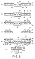
- Referring to Figs. 2(a) to 2(f), a semiconductor device according to a first embodiment of this invention will be successively described in the order of manufacturing processes. In Fig. 2(a), a
semiconductor chip 26 is at first prepared along with a base film sheet depicted at 35. Thesemiconductor chip 26 may be similar to that illustrated in Fig. 1 and has front and back chip surfaces directed upwards and downwards of Fig. 1(a), respectively. - The
base film sheet 35 is composed of an insulator material, namely, a nonconductive material, such as a polyimide resin. Like in Fig. 1, thebase film sheet 35 has a partitioned section or the partial zone which is defined by cut holes (not shown in Fig. 2) and which has a center region and a peripheral region surrounding the center region. Adevice hole 25 is bored in the center region and encompassed by the peripheral region. - Herein, it is to be noted that the illustrated peripheral region has first and second sheet surfaces directed upwards and downwards ie it has a top and a bottom surface and a plurality of via
holes 36 bored in thebase film sheet 35 and contiguous to the first and the second sheet surfaces. Such formation of the via holes 36 is different from that illustrated in Fig. 1. Such abase film sheet 35 may be called a perforated base film sheet. - As shown in Fig. 2(a), a plurality of
inner leads 28 are laid on the first sheet surface of thebase film sheet 35 and are extended from the peripheral region of thebase film sheet 35 inside of thedevice hole 25. Each of the inner leads 28 has an inside end positioned within thedevice hole 25 and an outside end placed on the first sheet surface of the peripheral region. - An electrode pad, namely, a
land 27 is formed on the outside end of eachinner lead 28 which is located on the viahole 36. A cover resistfilm 31 is coated on the first sheet surface of thebase film sheet 35 except for the land orpad 27. In other words, the electrode pads or lands 27 are not covered by the cover resistfilm 31. - On the other hand, the inside end of each
inner lead 28 is bonded onto the chip electrodes (depicted at 37) of thesemiconductor chip 26 and is therefore electrically connected to thesemiconductor chip 26 on the front chip surface. - As shown in Fig. 2(b), the
semiconductor chip 26 is molded on a side of the top chip surface together with the inner leads 28 extended within thedevice hole 25 by aresin mold 39. Thus, the top chip surface of thesemiconductor chip 26 is covered with theresin mold 39 along with bonded portions of the inner leads 28 while the bottom chip surface of thesemiconductor chip 26 is not covered with theresin mold 39, as illustrated in Fig. 2(b). In addition, thelands 27 are also not covered with the cover resistfilm 31 and are exposed to atmosphere. - On the exposed lands 27, ball shaped bumps40 are formed which are projected upwards of Fig. 2(c) and which may be called first bumps 40. The first bumps 40 may be, for example, solder and serve as outer connection electrode members. Thus, a base film member is obtained which includes the
base film sheet 35, thesemiconductor chip 26, and the first bumps 40. - In the illustrated example,.provision is made for a metal plate member, as shown in Fig. 2(d). The metal plate member comprises a
metal plate 45 which has a first (top) plate surface directed upwards of Fig. 2(d) and a second (bottom) plate surface directed downwards. In addition, themetal plate 45 is assumed to have a similar size to thebase film sheet 35 and has a center opening in a center area and a peripheral area surrounding the center opening. The center opening of themetal plate 45 may be identical with thedevice hole 25 of thebase film sheet 35 and can surround thesemiconductor chip 26 like thebase film sheet 35. Therefore, the illustratedmetal plate 45 can completely cover thebase film sheet 35. - On the first plate surface,
second bumps 47 are formed at positions which correspond to the via holes 36 on thebase film sheet 35. The second bumps 47 are composed of solder, like thefirst bumps 40 and are disposed onto the first plate surface so as to project upwards of Fig. 2 (d). The remaining portion of the first plate surface is covered with a solder resistfilm 48. - In Fig. 2(e), the base film member (shown in Fig. 2 (c)) and the metal plate member (shown in Fig. 2(d)) are reversed so that the
second bumps 47 on themetal plate 45 register with the via holes 36 on thebase film sheet 35. As a result, the top chip surface of thesemiconductor chip 26 is directed downwards of Fig. 2(e) while the bottom chip surface is directed upwards. Likewise, the first and the second plate surfaces of themetal plate 45 are directed downwards and upwards of Fig. 2(e), respectively. - Thereafter, the
second bumps 47 are brought into contact with the via holes 36 on thebase film sheet 35 and softened by a heat treatment. Consequently, thesecond bumps 47 are caused to partially flow into the corresponding viaholes 36 and are electrically connected to the inner leads 28 through the via holes 36. Thus, it is possible to obtain a semiconductor device which has the first and thesecond bumps base film sheet 35.Such bumps - In Fig. 2(f), a connection between the first and the
second bumps base film sheet 35 is covered with anadhesive film 49 on the side of thefirst bumps 40, as shown in Fig. 2(f). In addition, theland 27 is formed on theadhesive film 49 and is contacted with the first and thesecond bumps - Referring to Figs. 3(a) and (b), the semiconductor device illustrated in Fig. 2(e) is seen from the sides of the
first bumps 40 and themetal plate 45, respectively. As shown in Fig. 3(a), thefirst bumps 40 are arranged in a matrix manner on the peripheral region of thebase film sheet 35 around thesemiconductor chip 26 molded by theresin mold 39. The first bumps 40 are connected to the inner leads 28, as shown in Fig. 2(e) and are encompassed by the cover resistfilm 31, as illustrated in Fig. 3(a). In addition, the top chip surface of thesemiconductor chip 26 is covered with theresin mold 39, as is apparent from Fig. 3(a). - On the other hand, the bottom chip surface of the
semiconductor chip 26 is exposed on the side of themetal plate 45 without being covered with theresin mold 39 and themetal plate 45, as shown in Fig. 3(b). - Thus, the
semiconductor chip 26 molded is surrounded by themetal plate 45. The second bumps 47 are extended downwards of Fig. 3(b), as symbolized by broken line circles, and are small in number in comparison with thefirst bumps 40 shown in Fig. 3(a). This shows that thesecond bumps 47 are electrically connected only to a restricted number of the inner leads 28 and serve to supply the same potential to the restricted number of the inner leads 28. In other words, themetal plate 45 is operable to give a ground potential or a predetermined source potential to the restricted number of the inner leads 28. - With this structure, it is possible to reduce resistance or inductance of a power supply circuit by 1/5 - 1/10, by impressing the ground potential or the predetermined source potential, for example, Vcc onto the
metal plate 45. - Attachment of the
metal plate 45 to thebase film sheet 35 serves to electromagnetically shield the first bumps 40. Therefore, the semiconductor device is rarely influenced by an external noise. Moreover, thebase film sheet 35 has the via holes 36, which is useful to reduce warp or bend in thebase film sheet 35. - Referring to Figs. 4(a) and (b), a semiconductor device according to a second embodiment of this invention comprises a
metal plate 45a (Fig. 4(a)) which is different from that illustrated in Figs. 2 and 3. More specifically, the illustratedmetal plate 45a has no opening in the centre area thereof. Instead, asolder portion 50 of silver paste is located at the center area of themetal plate 45a. In addition, the cover resistfilm 48 is coated on the peripheral area of themetal plate 45a with the lands for thesecond bumps 47 left uncovered, like in Fig. 2. - As shown in Fig. 4(b), the
metal plate 45a illustrated in Fig. 4(a) is mounted on the base film member with thesecond bumps 47 directed downwards. Like in Fig. 2(c), the base film member has the via holes 36 and thesemiconductor chip 26 attached to thebase film sheet 35. - Thus, the base film member has a perforated
base film sheet 35 and thesecond bumps 47 are placed at positions which correspond to the via holes 36 of thebase film sheet 35. On the other hand, thesolder portion 50 is brought into contact with the back chip surface of thesemiconductor chip 26, as illustrated in Fig. 4(b). - Under the circumstances, the
second bumps 47 and thesolder portion 50 are subjected to a heat treatment to be softened or molten. The resultantsecond bumps 47 are caused to partially flow into the via holes 36 to be electrically connected to thelands 27 of the inner leads 28 while theresultant solder portion 50 mechanically connects themetal plate 45a to thesemiconductor chip 26. Thus, themetal plate 45a is mechanically fixed to thesemiconductor chip 26. - With this structure, the
metal plate 45a acts as a heat spreader for radiating heat from thesemiconductor chip 26 because themetal plate 45a is directly contacted with thesemiconductor chip 26. In addition, themetal plate 45a also serves as a shield plate like in Figs. 2 and 3 because elements in thesemiconductor chip 26 can be electromagnetically shielded by themetal plate 45a. - Furthermore, the
second bumps 47 may be connected to a predetermined or restricted number of the inner leads 28 when themetal plate 45a is given a predetermined potential, as mentioned in conjunction with Figs. 2 and 3. - As illustrated in Fig. 4(b), the first and the
second bumps base film sheet 35, like in Fig. 2. - Referring to Fig. 5, a semiconductor device according to a third embodiment of this invention is similar to that illustrated in Figs. 4(a) and (b) except that a
metal plate 45b has a plurality of throughholes 52 which correspond to the via holes 36 formed in thebase film sheet 35. Themetal plate 45b lends itself to a heat spreader like themetal plate 45a shown in Figs. 4(a) and (b). - The illustrated semiconductor device can be manufactured by preparing the
base film sheet 35 which has the via holes 36 and the first and the second sheet surfaces directed downwards and upwards of Fig. 5, respectively, and by projecting the first and thesecond bumps base film sheet 35, respectively. In this case, the first and thesecond bumps - As shown in Fig. 5, the
second bumps 47 are partially introduced into the throughholes 52 formed within themetal plate 45b. In this case, tops of thesecond bumps 47 can be seen on an upper side of Fig. 5 and can be contacted by the use of an electric testing probe (not shown). This means that the illustrated semiconductor device can be checked even after the semiconductor device is mounted on a circuit board (not shown). Incidentally, the first and thesecond bumps film 31, like in the other figures. - Referring to Fig. 6, a semiconductor device according to a fourth embodiment of this invention has a structure similar to that illustrated in Figs. 2(a) to (f) in view of the fact that two semiconductor devices as shown in Figs. 2(a) to (f) are stacked in a thickness direction of
semiconductor chips 26 and 26'.
Accordingly, similar reference numerals will be attached to the corresponding portions and elements for a better understanding of this invention. In this case, the two semiconductor devices are similar in structure to each other and will be called first and second semiconductor units hereinunder. - More particularly, the first semiconductor unit includes the
base film sheet 35 having the via holes 36, thesemiconductor chip 26 molded by theresin mold 39, and the inner leads 28 connected to thechip electrodes 37 and thelands 27 formed on thebase film sheet 35. In the first semiconductor unit, bumps 40 are mounted on thelands 27 as first unit bumps and projected from thelands 27 downwards of Fig. 6. - On the via holes 36 of the
base film sheet 35, bumps 40' are located and may be called second unit bumps. The second unit bumps 40' are electrically connected to the first unit bumps 40 through the via holes 36 bored within thebase film sheet 35 of the first semiconductor unit. - As is apparent from Fig. 6, the second semiconductor unit includes, together with the second unit bumps 40', the base film sheet 35' having the via holes 36', the semiconductor chip 26' molded by the resin mold 39', and the inner lands 28'. The second unit bumps 40' are directed downwards of Fig. 6 and are connected to the first unit bumps 40 through the via holes 36 formed within the
base film sheet 35, as mentioned before. - The via holes 36' of the second semiconductor unit are located at positions from which the second unit bumps 40' are projected. In this event, all of the via holes 36' may not be located at the positions of the second unit bumps 40', although not shown in Fig. 6.
- In the illustrated example, a metal plate member is mounted on the second semiconductor unit and is similar in structure to that illustrated in Fig. 2(d). Specifically, the metal plate member includes the
metal plate 45 and thebumps 47 surrounded by the cover resistfilm 48. Thebumps 47 are electrically connected to the bumps 40' of the second semiconductor unit through the via holes 36' formed within the base film sheet 35'. - With this structure, an electric potential can be given to the inner leads 28 and 28' electrically connected to the
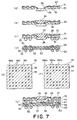
bumps - Referring to Fig. 7(a) to (g), a semiconductor device is manufactured through processes illustrated in Figs. 7(a) through (d). In Fig. 7(a), a
base film sheet 35 is prepared which has upper and lower surfaces, a plurality of viaholes 36 and adevice hole 25, like in Fig. 2. Inner leads 28 are laid on an upper surface of thebase film sheet 35 and are electrically connected to chip electrodes of asemiconductor chip 26 and lands 27 formed on the via holes 36. Thus, thesemiconductor chip 26 is fixed to thebase film sheet 35 by the inner leads 28. A cover resistfilm 31 is formed on the upper surface of thebase film sheet 35 with thelands 27 exposed - The
semiconductor chip 26 is molded by aresin mold 39 on the front chip surface directed upwards of Fig. 7(b). As illustrated in Fig. 7(b), theresin mold 39 covers the top chip surface of thesemiconductor chip 26 but does not cover the bottom chip surface. - As shown in Fig. 7(c), bumps 40 which may be called first bumps are projected from the lower surface of the
base film sheet 35 downwards and are electrically connected to thelands 27 formed on the upper surface of thebase film sheet 35. Thus, thefirst bumps 40 illustrated in Fig. 7(c) have portions buried into the via holes 36 and portions projected from thebase film sheet 35. The illustrated lands 27 are not covered by the cover resistfilm 31 and are therefore exposed to atmosphere. - Furthermore, a
circuit board 55 which may be formed by ceramics, glass epoxy, is prepared as shown in Fig. 7(d). The illustratedcircuit board 55 is formed by a multilayer printed circuit board which includes asource layer 56 and aground layer 57 wired within theboard 55. Thesource layer 56 is electrically connected to firstspecific lands 61 placed on both upper and lower board surfaces of thecircuit board 55 while theground layer 57 is electrically connected to secondspecific lands 62 placed on both surfaces of thecircuit board 55. The upper and the lower board surfaces may be referred to as first and second board surfaces, respectively. To the lands formed on the lower board surface of thecircuit board 55, ball bumps 63 of, for example, solder are attached as external connection electrode members and may be referred to as second bumps, like in the previous embodiments. - It is to be noted here that the
first bumps 40 on thebase film sheet 35 include bumps for an electric source, bumps for ground, and bumps for transferring information signals. In this event, the bumps for the electric source and the bumps for the ground can use the source and the ground layers 56 and 57 in common, respectively. Therefore, thesecond bumps 63 projected from thecircuit board 55 may be reduced in. number as compared with thefirst bumps 40 projected from thebase film sheet 35. - Referring to Figs. 7(e) and (f), the
source layer 56 and theground layer 57 in thecircuit board 55 will be described in detail. In Fig. 7(e), thesource layer 56 has a plurality of via holes as collectively depicted at 58. The via holes 58 include viaholes holes 581 for the electric source are electrically connected to thesource layer 56, as shown by single circles, while the remaining viaholes source layer 56. Specifically, thesource layer 56, as shown by double circles. - Herein, the via
holes 581 are electrically connected to thebumps 40 for the electric source while the viaholes bumps 40 for the ground and the information signals. Under the circumstances, thesource layer 56 is electrically connected only to thebumps 40 for the electric source and is disconnected to thebumps 40 for the ground and the information signals. - In Fig. 7(f), the
ground layer 57 has also viaholes holes 582a for the ground are electrically connected to theground layer 57 while the remaining viaholes ground layer 57, as readily understood from Fig. 7(f). - Referring to Fig. 7(g), the base film member illustrated in Fig. 7(c) is mounted on the
circuit board 55 shown in Fig. 7(d). In this event, the base film member is positioned on thecircuit board 55 so that thefirst bumps 40 are brought into contact with thelands 61 of thecircuit board 55. Thus, thefirst bumps 40 of the base film member are electrically connected to thesecond bumps 63 on thecircuit board 55. - In the example illustrated in Figs. 7(a) through (g), the
lands 27 on thebase film sheet 35 are exposed to atmosphere and may be therefore visibly observed and contacted by a bonding tool or an electric testing probe. Therefore, the illustrated semiconductor device can be bonded by the bonding tool onto any other circuit board or tested by the testing probe after it is bonded. - In addition, ground and source electrodes formed by the
bumps 40 are unified into single ground and source layers 57 and 56, respectively, in thecircuit board 55 placed under the base film member. This structure makes it possible to reduce resistance and inductance values of the ground and the source electrodes by 30% - 50%. Moreover, thecircuit board 55 serves as a heat spreader and can reduce a thermal resistance to 10°C /W. Like in the other embodiments, it is possible to avoid warping of thebase film sheet 35 because the via holes 40 are bored in thebase film sheet 35. - Referring to Figs. 8(a) to (e), another semiconductor device will be described with reference to its manufacturing processes. In Figs. 8(a) and (b), the
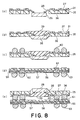
semiconductor chip 26 is attached to the inner leads 28 extended into thedevice hole 25 of thebase film sheet 35 and is molded by theresin mold 39, like in Figs. 7(a) and (b). It is needless to say that the illustratedbase film sheet 35 also has the via holes 36 bored within the peripheral region thereof and thelands 27 which are formed at the ends of the inner leads 28 and which are not covered by the cover resistfilm 31 as already described. - Herein, it is noted in Fig. 8(c) that the
base film sheet 35 has the front sheet surface and the back sheet surface directed upwards and downwards of Fig. 8(c), respectively, andfirst bumps 40 projected from thelands 27 of the front sheet surface in an upper direction of Fig. 7(c). As a result, thefirst bumps 40 are projected in the direction different from that illustrated in Fig. 7(c). In this connection, the via holes 36 are not filled with thefirst bumps 40 and thelands 27 can be viewed through the via holes 36. Thus, a base film member is obtained which is somewhat different from that shown in Fig. 7(c). - In Fig. 8(d), a
circuit board 55 is prepared which is similar in structure to that illustrated in Fig. 7(d). Specifically, thecircuit board 55 has thesource layer 56 and theground layer 57 therein and thelands circuit board 55 and electrically connected to the source and the ground layers 56 and 57. On thelands 62 directed downwards of Fig. 8(d), board bumps 63 are formed to mount thecircuit board 55 onto a mother board or so and may be called second bumps. - As shown in Fig. 8(e), the base film member illustrated in Fig. 8(c) is reversed so that the
first bumps 40 register with thelands 61 of thecircuit board 55. Thereafter, the base film member and thecircuit board 55 are adjusted to each other to locate thefirst bumps 40 on thelands 61 of thecircuit board 55. Under the circumstances, thefirst bumps 40 are softened by a heat treatment to be fixed to thelands 61. Thus, the base film member is mounted on thecircuit board 55 and the semiconductor device is completed. - With this structure, the back chip surface of the
semiconductor chip 26 and the via holes 36 are exposed to atmosphere Consequently, thelands 27 can be visibly observed through the via holes 36 and can be directly touched with the electric testing probe or the like. Therefore, each of the inner leads 28 can be electrically tested through the via holes 36 even after the base film member is mounted on thecircuit board 55 or after thecircuit board 55 is mounted on the mother board. - Referring to Figs. 9(a) to (c), these figures illustrate a semiconductor device similar in structure to that illustrated in Fig. 8 except that the
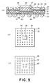
first bumps 40 in Fig. 8 are eliminated from Fig. 9 and that thecircuit board 55 illustrated in Fig. 9 (a) has a recessed portion, namely, acavity portion 65 at the center region thereof and asilver paste 66 filled in the cavity portion. - More specifically, the
lands 61 are formed on an upper board surface of thecircuit board 55 while thesemiconductor chip 26 is located within the device hole of thebase film sheet 35 and is molded by theresin mold 39 with the top chip surface of thesemiconductor chip 26 directed upwards of Fig. 9(a). Like in Fig. 8(b), thelands 27 are exposed to atmosphere and can be seen through the via holes 36. In Fig. 9(a), the base film member is directly located on thecircuit board 55 without any bumps interposed. In this event, theresin mold 39 is brought into contact with thesilver paste 65. Consequently, the base film member is in close contact with thecircuit board 55. - On the other hand, the
lands 27 of the inner leads 28 are directly bonded to thelands 61 on thecircuit board 55 by the use of a bonding tool to formbonding portions 70. Such bonding portions can be formed by inserting the bonding tool into the via holes 36 and by bonding thelands 27 or the inner leads 28 to thelands 61 by a single point method. Accordingly, thebonding portions 70 can be seen through the via holes 36 of thebase film sheet 35, as illustrated in Fig. 9(b). - With this structure, the
second bumps 63 on thecircuit board 55 include bumps which are thermally coupled through thermal via holes of thecircuit board 55 to thesilver paste 66 filled in thecavity portion 65. In order to improve a heat radiation characteristic of the semiconductor device, dummy bumps 63' may be included in thesecond bumps 63, as shown in Fig. 9(c). - At any rate, the
semiconductor chip 26 is thermally coupled to thecircuit board 55 through thesilver paste 66. Therefore, heat is effectively radiated from thesemiconductor chip 26 through thecircuit board 55. - Referring to Fig. 10, this figure illustrates a semiconductor device similar to that illustrated in Fig. 9(a) except that the bottom chip surface of the semiconductor chip 26 (Fig. 10) is brought into contact with the
silver paste 66 filled in thecavity portion 65 formed in thecircuit board 55. In this case, the top chip surface of thesemiconductor chip 26 is directed upwards of Fig. 10 and covered with theresin mold 39, as shown in Fig. 10. In other words, thesemiconductor chip 26 illustrated in Fig. 10 is reversed relative to that illustrated in Fig. 9 and mounted on thecavity portion 65 of thecircuit board 55. - In the illustrated example, the
lands 62 which are formed on a lower board surface of thecircuit board 55 to mount thesecond bumps 63 and are extended through thecircuit board 55 into the via holes 36 bored in thebase film sheet 35. In other words, thelands 62 are projected into the via holes 36 in the form of electrode pins 69 which are electrically connected to the inner leads 28. In addition, thesecond bumps 63 include bumps which are thermally coupled to thesilver paste 66 in thecavity portion 65, which serves to improve the heat radiation characteristic. - It is to be noted in connection with all embodiments that the via holes 36 have internal side surfaces which are not covered by any conduction materials.
- While this invention has far been described in conjunction with several embodiments thereof, it will readily be possible for those skilled in the art to put this invention into practice in various other manners. For example, the
circuit board 55 may include pins in lieu of thesecond bumps 63 illustrated in Figs. 7 through 10. Thus, it is possible to improve electric and thermal characteristics and/or to increase a packing density by forming via holes in the base film sheet.
Claims (7)
- A semiconductor device, comprising:a base film sheet (35) which has a center region, a device hole (25) in said center region, a peripheral region surrounding said center region, and a plurality of via holes (36) bored on the peripheral region;a semiconductor chip attached to said base film sheet in said device hole of said center region;an electric connection member which is laid on said peripheral region and electrically connected to said semiconductor chip, said electric connection member comprising a plurality of lands (27) arranged on said peripheral portion of said base film sheet and located at the position of said plurality of said via holes, and a plurality of inner leads (28) connected to said lands and said semiconductor chip;an outer electrode member which has a portion positioned at said plurality of via holes and which is electrically connected to said electric connection member, said outer electrode member comprising a plurality of first bumps (40) mounted on said lands and projecting from said base film sheet; anda metal plate member (45) electrically connected to said first bumps through said plurality of via holes, said metal plate member comprising a plate surface and a plurality of second bumps (47) attached to said plate surface facing said via holes of said base film sheet and electrically connected to said first bumps through said via holes, said metal plate having a center area, a peripheral area which surrounds said center area on said plate surface, and a hole formed on said center area and covering the peripheral region of said base film sheet with said semiconductor chip left uncovered, said second bumps being formed on said peripheral area and projecting towards said base film sheet.
- A semiconductor device, comprising:a base film sheet (35) which has a center region, a device hole (25) in said center region, a peripheral region surrounding said center region, and a plurality of via holes (36) bored on the peripheral region;a semiconductor chip (26) attached to said base film sheet in said device hole of said center region;an electric connection member which is laid on said peripheral region and electrically connected to said semiconductor chip, said electric connection member comprising a plurality of lands (27) arranged on said peripheral portion of said base film sheet and located at the position of said plurality of said via holes, and a plurality of inner leads (28) connected to said lands and said semiconductor chip;an outer electrode member which has a portion positioned at said plurality of via holes and which is electrically connected to said electric connection member, said outer electrode member comprising a plurality of first bumps (40) mounted on said lands and projecting from said base film sheet; anda metal plate member (45a; 45b) electrically connected to said first bumps through said plurality of via holes, said metal plate member comprising a plate surface and a plurality of second bumps (47) attached to said plate surface facing said via holes of said base film sheet and electrically connected to said first bumps through said via holes, said metal plate having on the plate surface a center area, a peripheral area surrounding said center area, and a solder layer (50) which is formed on said center area and which is brought into contact with said semiconductor chip, said second bumps being formed on said peripheral area and projecting towards said base film sheet.
- A semiconductor device as claimed in claim 2, wherein said metal plate (45b) has a plurality of through holes (52) on said peripheral area, said second bumps extending into said through holes.
- A semiconductor device according to any preceding claim, wherein the metal plate member is electrically grounded.
- A semiconductor device according to any of Claims 1 to 3, wherein the metal plate member is connected to a source of electrical potential.
- A semiconductor device according to any preceding claim, wherein the metal plate member serves to electromagnetically shield the first bumps (40).
- A stacked semiconductor device comprising a first semiconductor device according to any preceding claim and a second semiconductor device stacked to the first semiconductor device via said first bumps so as to be electrically connected to the first semiconductor device.
Applications Claiming Priority (3)
| Application Number | Priority Date | Filing Date | Title |
|---|---|---|---|
| JP236985/94 | 1994-09-30 | ||
| JP23698594 | 1994-09-30 | ||
| JP6236985A JP2780649B2 (en) | 1994-09-30 | 1994-09-30 | Semiconductor device |
Publications (3)
| Publication Number | Publication Date |
|---|---|
| EP0704897A2 EP0704897A2 (en) | 1996-04-03 |
| EP0704897A3 EP0704897A3 (en) | 1997-07-16 |
| EP0704897B1 true EP0704897B1 (en) | 2002-02-13 |
Family
ID=17008691
Family Applications (1)
| Application Number | Title | Priority Date | Filing Date |
|---|---|---|---|
| EP95306885A Expired - Lifetime EP0704897B1 (en) | 1994-09-30 | 1995-09-29 | Semiconductor device with metal plate |
Country Status (5)
| Country | Link |
|---|---|
| US (1) | US5763939A (en) |
| EP (1) | EP0704897B1 (en) |
| JP (1) | JP2780649B2 (en) |
| KR (1) | KR100241572B1 (en) |
| DE (1) | DE69525406T2 (en) |
Families Citing this family (87)
| Publication number | Priority date | Publication date | Assignee | Title |
|---|---|---|---|---|
| US5677566A (en) * | 1995-05-08 | 1997-10-14 | Micron Technology, Inc. | Semiconductor chip package |
| JP2899540B2 (en) * | 1995-06-12 | 1999-06-02 | 日東電工株式会社 | Film carrier and semiconductor device using the same |
| JP2891665B2 (en) * | 1996-03-22 | 1999-05-17 | 株式会社日立製作所 | Semiconductor integrated circuit device and method of manufacturing the same |
| US20040061220A1 (en) * | 1996-03-22 | 2004-04-01 | Chuichi Miyazaki | Semiconductor device and manufacturing method thereof |
| JP2755252B2 (en) * | 1996-05-30 | 1998-05-20 | 日本電気株式会社 | Semiconductor device package and semiconductor device |
| JP2770820B2 (en) * | 1996-07-01 | 1998-07-02 | 日本電気株式会社 | Semiconductor device mounting structure |
| US5759737A (en) * | 1996-09-06 | 1998-06-02 | International Business Machines Corporation | Method of making a component carrier |
| US5909058A (en) * | 1996-09-25 | 1999-06-01 | Kabushiki Kaisha Toshiba | Semiconductor package and semiconductor mounting part |
| KR100209760B1 (en) * | 1996-12-19 | 1999-07-15 | 구본준 | Semiconductor package and its manufacturing method |
| JP2982729B2 (en) * | 1997-01-16 | 1999-11-29 | 日本電気株式会社 | Semiconductor device |
| JP2924840B2 (en) * | 1997-02-13 | 1999-07-26 | 日本電気株式会社 | Tape-BGA type semiconductor device |
| JPH10335580A (en) * | 1997-06-02 | 1998-12-18 | Mitsubishi Electric Corp | Semiconductor package and semiconductor module using it |
| US5986209A (en) * | 1997-07-09 | 1999-11-16 | Micron Technology, Inc. | Package stack via bottom leaded plastic (BLP) packaging |
| JP3834426B2 (en) | 1997-09-02 | 2006-10-18 | 沖電気工業株式会社 | Semiconductor device |
| US6573609B2 (en) | 1997-11-25 | 2003-06-03 | Tessera, Inc. | Microelectronic component with rigid interposer |
| US6002168A (en) * | 1997-11-25 | 1999-12-14 | Tessera, Inc. | Microelectronic component with rigid interposer |
| JP3310617B2 (en) * | 1998-05-29 | 2002-08-05 | シャープ株式会社 | Resin-sealed semiconductor device and method of manufacturing the same |
| KR100266693B1 (en) * | 1998-05-30 | 2000-09-15 | 김영환 | Stackable ball grid array semiconductor package and fabrication method thereof |
| US6300679B1 (en) * | 1998-06-01 | 2001-10-09 | Semiconductor Components Industries, Llc | Flexible substrate for packaging a semiconductor component |
| US6451624B1 (en) | 1998-06-05 | 2002-09-17 | Micron Technology, Inc. | Stackable semiconductor package having conductive layer and insulating layers and method of fabrication |
| US6020629A (en) * | 1998-06-05 | 2000-02-01 | Micron Technology, Inc. | Stacked semiconductor package and method of fabrication |
| TW411537B (en) * | 1998-07-31 | 2000-11-11 | Siliconware Precision Industries Co Ltd | Semiconductor package with CSP-BGA structure |
| US6031282A (en) * | 1998-08-27 | 2000-02-29 | Advantest Corp. | High performance integrated circuit chip package |
| US6051887A (en) * | 1998-08-28 | 2000-04-18 | Medtronic, Inc. | Semiconductor stacked device for implantable medical apparatus |
| US6084297A (en) * | 1998-09-03 | 2000-07-04 | Micron Technology, Inc. | Cavity ball grid array apparatus |
| FR2785722A1 (en) * | 1998-11-06 | 2000-05-12 | Bull Sa | THREE-DIMENSIONAL INTERCONNECTION STRUCTURE OF MULTIPLE CIRCUITS TO FORM A MULTI-COMPONENT PACKAGE |
| US6069407A (en) * | 1998-11-18 | 2000-05-30 | Vlsi Technology, Inc. | BGA package using PCB and tape in a die-up configuration |
| JP2000243876A (en) * | 1999-02-23 | 2000-09-08 | Fujitsu Ltd | Semiconductor device and its manufacture |
| US6982478B2 (en) * | 1999-03-26 | 2006-01-03 | Oki Electric Industry Co., Ltd. | Semiconductor device and method of fabricating the same |
| US6636334B2 (en) * | 1999-03-26 | 2003-10-21 | Oki Electric Industry Co., Ltd. | Semiconductor device having high-density packaging thereof |
| JP3844936B2 (en) * | 1999-03-26 | 2006-11-15 | 富士通株式会社 | Semiconductor device |
| JP3576030B2 (en) * | 1999-03-26 | 2004-10-13 | 沖電気工業株式会社 | Semiconductor device and manufacturing method thereof |
| JP3575001B2 (en) * | 1999-05-07 | 2004-10-06 | アムコー テクノロジー コリア インコーポレーティド | Semiconductor package and manufacturing method thereof |
| USRE40112E1 (en) | 1999-05-20 | 2008-02-26 | Amkor Technology, Inc. | Semiconductor package and method for fabricating the same |
| JP3398721B2 (en) * | 1999-05-20 | 2003-04-21 | アムコー テクノロジー コリア インコーポレーティド | Semiconductor package and manufacturing method thereof |
| DE19923523B4 (en) * | 1999-05-21 | 2004-09-30 | Infineon Technologies Ag | Semiconductor module with semiconductor chips arranged one above the other and connected to one another |
| JP2001077301A (en) * | 1999-08-24 | 2001-03-23 | Amkor Technology Korea Inc | Semiconductor package and its manufacturing method |
| US6756253B1 (en) * | 1999-08-27 | 2004-06-29 | Micron Technology, Inc. | Method for fabricating a semiconductor component with external contact polymer support layer |
| US6118179A (en) * | 1999-08-27 | 2000-09-12 | Micron Technology, Inc. | Semiconductor component with external contact polymer support member and method of fabrication |
| US6210992B1 (en) * | 1999-08-31 | 2001-04-03 | Micron Technology, Inc. | Controlling packaging encapsulant leakage |
| US6303981B1 (en) | 1999-09-01 | 2001-10-16 | Micron Technology, Inc. | Semiconductor package having stacked dice and leadframes and method of fabrication |
| US6645794B2 (en) | 2000-10-18 | 2003-11-11 | Hitachi, Ltd. | Method of manufacturing a semiconductor device by monolithically forming a sealing resin for sealing a chip and a reinforcing frame by transfer molding |
| US6564454B1 (en) | 2000-12-28 | 2003-05-20 | Amkor Technology, Inc. | Method of making and stacking a semiconductor package |
| DE10110203B4 (en) * | 2001-03-02 | 2006-12-14 | Infineon Technologies Ag | Electronic component with stacked semiconductor chips and method for its production |
| KR100781146B1 (en) * | 2001-08-09 | 2007-11-30 | 삼성테크윈 주식회사 | BGA semiconductor package using TAB bonding and the fabrication method thereof |
| WO2003019654A1 (en) * | 2001-08-22 | 2003-03-06 | Tessera, Inc. | Stacked chip assembly with stiffening layer |
| US20030038356A1 (en) * | 2001-08-24 | 2003-02-27 | Derderian James M | Semiconductor devices including stacking spacers thereon, assemblies including the semiconductor devices, and methods |
| US6882034B2 (en) * | 2001-08-29 | 2005-04-19 | Micron Technology, Inc. | Routing element for use in multi-chip modules, multi-chip modules including the routing element, and methods |
| US6611052B2 (en) | 2001-11-16 | 2003-08-26 | Micron Technology, Inc. | Wafer level stackable semiconductor package |
| US6885107B2 (en) * | 2002-08-29 | 2005-04-26 | Micron Technology, Inc. | Flip-chip image sensor packages and methods of fabrication |
| US6737742B2 (en) * | 2002-09-11 | 2004-05-18 | International Business Machines Corporation | Stacked package for integrated circuits |
| JP3891123B2 (en) * | 2003-02-06 | 2007-03-14 | セイコーエプソン株式会社 | SEMICONDUCTOR DEVICE, ELECTRONIC DEVICE, ELECTRONIC DEVICE, AND SEMICONDUCTOR DEVICE MANUFACTURING METHOD |
| US7191516B2 (en) * | 2003-07-16 | 2007-03-20 | Maxwell Technologies, Inc. | Method for shielding integrated circuit devices |
| US6936922B1 (en) | 2003-09-26 | 2005-08-30 | Amkor Technology, Inc. | Semiconductor package structure reducing warpage and manufacturing method thereof |
| US20070145548A1 (en) * | 2003-12-22 | 2007-06-28 | Amkor Technology, Inc. | Stack-type semiconductor package and manufacturing method thereof |
| US7009296B1 (en) | 2004-01-15 | 2006-03-07 | Amkor Technology, Inc. | Semiconductor package with substrate coupled to a peripheral side surface of a semiconductor die |
| JP2005223036A (en) * | 2004-02-04 | 2005-08-18 | Alps Electric Co Ltd | Electronic part and its manufacturing method |
| KR100688500B1 (en) * | 2004-09-06 | 2007-03-02 | 삼성전자주식회사 | Multi stack package having dummy package substrate for protection of semiconductor chip and method of fabricating the same |
| US7183638B2 (en) * | 2004-12-30 | 2007-02-27 | Intel Corporation | Embedded heat spreader |
| TW200636946A (en) * | 2005-04-12 | 2006-10-16 | Advanced Semiconductor Eng | Chip package and packaging process thereof |
| DE102005039365B4 (en) * | 2005-08-19 | 2022-02-10 | Infineon Technologies Ag | Gate-controlled fin resistive element operating as a pinch - resistor for use as an ESD protection element in an electrical circuit and a device for protecting against electrostatic discharges in an electrical circuit |
| JP2007201254A (en) * | 2006-01-27 | 2007-08-09 | Ibiden Co Ltd | Built-in semiconductor-element including board, and built-in semiconductor-element including multilayer circuit board |
| US7652361B1 (en) | 2006-03-03 | 2010-01-26 | Amkor Technology, Inc. | Land patterns for a semiconductor stacking structure and method therefor |
| US9466545B1 (en) | 2007-02-21 | 2016-10-11 | Amkor Technology, Inc. | Semiconductor package in package |
| TWI335070B (en) * | 2007-03-23 | 2010-12-21 | Advanced Semiconductor Eng | Semiconductor package and the method of making the same |
| TWI473553B (en) | 2008-07-03 | 2015-02-11 | Advanced Semiconductor Eng | Chip package structure |
| US8012797B2 (en) * | 2009-01-07 | 2011-09-06 | Advanced Semiconductor Engineering, Inc. | Method for forming stackable semiconductor device packages including openings with conductive bumps of specified geometries |
| US20100171206A1 (en) * | 2009-01-07 | 2010-07-08 | Chi-Chih Chu | Package-on-Package Device, Semiconductor Package, and Method for Manufacturing The Same |
| TWI499024B (en) * | 2009-01-07 | 2015-09-01 | Advanced Semiconductor Eng | Package-on-package device, semiconductor package and method for manufacturing the same |
| US20110024899A1 (en) * | 2009-07-28 | 2011-02-03 | Kenji Masumoto | Substrate structure for cavity package |
| TWI469283B (en) * | 2009-08-31 | 2015-01-11 | Advanced Semiconductor Eng | Package structure and package process |
| JP5574667B2 (en) * | 2009-10-21 | 2014-08-20 | キヤノン株式会社 | Package, semiconductor device, manufacturing method and equipment thereof |
| US8198131B2 (en) * | 2009-11-18 | 2012-06-12 | Advanced Semiconductor Engineering, Inc. | Stackable semiconductor device packages |
| TWI408785B (en) * | 2009-12-31 | 2013-09-11 | Advanced Semiconductor Eng | Semiconductor package |
| US8569894B2 (en) | 2010-01-13 | 2013-10-29 | Advanced Semiconductor Engineering, Inc. | Semiconductor package with single sided substrate design and manufacturing methods thereof |
| TWI419283B (en) * | 2010-02-10 | 2013-12-11 | Advanced Semiconductor Eng | Package structure |
| TWI411075B (en) | 2010-03-22 | 2013-10-01 | Advanced Semiconductor Eng | Semiconductor package and manufacturing method thereof |
| CN102201382B (en) * | 2010-03-26 | 2013-01-23 | 日月光半导体制造股份有限公司 | Semiconductor packaging piece and manufacturing method thereof |
| US8278746B2 (en) * | 2010-04-02 | 2012-10-02 | Advanced Semiconductor Engineering, Inc. | Semiconductor device packages including connecting elements |
| US8624374B2 (en) | 2010-04-02 | 2014-01-07 | Advanced Semiconductor Engineering, Inc. | Semiconductor device packages with fan-out and with connecting elements for stacking and manufacturing methods thereof |
| TWI451546B (en) | 2010-10-29 | 2014-09-01 | Advanced Semiconductor Eng | Stacked semiconductor package, semiconductor package thereof and method for making a semiconductor package |
| KR20120068216A (en) * | 2010-12-17 | 2012-06-27 | 에스케이하이닉스 주식회사 | Semiconductor integrated circuit |
| TWI445155B (en) | 2011-01-06 | 2014-07-11 | Advanced Semiconductor Eng | Stacked semiconductor package and method for making the same |
| US9171792B2 (en) | 2011-02-28 | 2015-10-27 | Advanced Semiconductor Engineering, Inc. | Semiconductor device packages having a side-by-side device arrangement and stacking functionality |
| US9557370B2 (en) * | 2012-02-10 | 2017-01-31 | Taiwan Semiconductor Manufacturing Company, Ltd. | Methods of improving bump allocation for semiconductor devices and semiconductor devices with improved bump allocation |
| CN103050450B (en) * | 2012-11-14 | 2015-10-28 | 日月光半导体制造股份有限公司 | Chip encapsulation construction and manufacture method thereof |
| US20150132148A1 (en) | 2013-11-13 | 2015-05-14 | Reza Afshar | Dual speed motor controller and method for operation thereof |
Family Cites Families (8)
| Publication number | Priority date | Publication date | Assignee | Title |
|---|---|---|---|---|
| JPS6057222B2 (en) * | 1980-03-26 | 1985-12-13 | シャープ株式会社 | Film carrier type semiconductor device |
| JPH02252251A (en) * | 1989-03-27 | 1990-10-11 | Nec Corp | Film carrier tape |
| US5045914A (en) * | 1989-12-26 | 1991-09-03 | Motorola, Inc. | Plastic pad array electronic AC device |
| US5045921A (en) * | 1989-12-26 | 1991-09-03 | Motorola, Inc. | Pad array carrier IC device using flexible tape |
| JPH03272152A (en) * | 1990-03-22 | 1991-12-03 | Fujitsu Ltd | Semiconductor package |
| JPH0694881A (en) | 1992-09-10 | 1994-04-08 | Hitachi Ltd | Emergency cooling system for atomic reactor |
| US5291062A (en) * | 1993-03-01 | 1994-03-01 | Motorola, Inc. | Area array semiconductor device having a lid with functional contacts |
| JPH06268101A (en) * | 1993-03-17 | 1994-09-22 | Hitachi Ltd | Semiconductor device and its manufacture, electronic device, lead frame, and mounting substrate |
-
1994
- 1994-09-30 JP JP6236985A patent/JP2780649B2/en not_active Expired - Fee Related
-
1995
- 1995-09-18 US US08/529,341 patent/US5763939A/en not_active Expired - Fee Related
- 1995-09-27 KR KR1019950032155A patent/KR100241572B1/en not_active IP Right Cessation
- 1995-09-29 DE DE69525406T patent/DE69525406T2/en not_active Expired - Fee Related
- 1995-09-29 EP EP95306885A patent/EP0704897B1/en not_active Expired - Lifetime
Also Published As
| Publication number | Publication date |
|---|---|
| DE69525406D1 (en) | 2002-03-21 |
| JPH08111433A (en) | 1996-04-30 |
| DE69525406T2 (en) | 2002-11-07 |
| JP2780649B2 (en) | 1998-07-30 |
| KR100241572B1 (en) | 2000-02-01 |
| US5763939A (en) | 1998-06-09 |
| EP0704897A2 (en) | 1996-04-03 |
| EP0704897A3 (en) | 1997-07-16 |
Similar Documents
| Publication | Publication Date | Title |
|---|---|---|
| EP0704897B1 (en) | Semiconductor device with metal plate | |
| US5399903A (en) | Semiconductor device having an universal die size inner lead layout | |
| KR900003828B1 (en) | Semiconductor device and manufacturing method thereof | |
| US5620928A (en) | Ultra thin ball grid array using a flex tape or printed wiring board substrate and method | |
| EP0684641B1 (en) | Semiconductor device moulding capable of accomplishing a high moisture proof | |
| KR100899314B1 (en) | Semiconductor device and method of manufacturing the same | |
| KR970004217B1 (en) | Semiconductor device | |
| US6359341B1 (en) | Ball grid array integrated circuit package structure | |
| KR100716871B1 (en) | Carrier frame for semiconductor package and semiconductor package using it and its manufacturing method | |
| US6468834B1 (en) | Method of fabricating a BGA package using PCB and tape in a die-up configuration | |
| JP2744685B2 (en) | Semiconductor device | |
| US6046495A (en) | Semiconductor device having a tab tape and a ground layer | |
| US6201298B1 (en) | Semiconductor device using wiring tape | |
| US5168345A (en) | Semiconductor device having a universal die size inner lead layout | |
| US6166435A (en) | Flip-chip ball grid array package with a heat slug | |
| US6037656A (en) | Semiconductor integrated circuit device having short signal paths to terminals and process of fabrication thereof | |
| US5910686A (en) | Cavity down HBGA package structure | |
| US4831495A (en) | Unitized packaging arrangement for an energy dissipating device | |
| US6844219B2 (en) | Semiconductor device and lead frame therefor | |
| JP3450477B2 (en) | Semiconductor device and manufacturing method thereof | |
| KR100216063B1 (en) | Metal ball grid array package | |
| JPH0786335A (en) | Semiconductor mounting structure and resin-sealed semiconcuctor device used therein | |
| JPH08250529A (en) | Plastic molded type semiconductor device and manufacture thereof | |
| JPH09148482A (en) | Semiconductor device | |
| JP4122560B2 (en) | Semiconductor device and mounting structure of semiconductor device |
Legal Events
| Date | Code | Title | Description |
|---|---|---|---|
| PUAI | Public reference made under article 153(3) epc to a published international application that has entered the european phase |
Free format text: ORIGINAL CODE: 0009012 |
|
| AK | Designated contracting states |
Kind code of ref document: A2 Designated state(s): DE FR GB |
|
| PUAL | Search report despatched |
Free format text: ORIGINAL CODE: 0009013 |
|
| AK | Designated contracting states |
Kind code of ref document: A3 Designated state(s): DE FR GB |
|
| 17P | Request for examination filed |
Effective date: 19970802 |
|
| 17Q | First examination report despatched |
Effective date: 19980924 |
|
| RTI1 | Title (correction) |
Free format text: BGA SEMICONDUCTOR DEVICE WITH METAL PLATE |
|
| GRAG | Despatch of communication of intention to grant |
Free format text: ORIGINAL CODE: EPIDOS AGRA |
|
| GRAG | Despatch of communication of intention to grant |
Free format text: ORIGINAL CODE: EPIDOS AGRA |
|
| GRAH | Despatch of communication of intention to grant a patent |
Free format text: ORIGINAL CODE: EPIDOS IGRA |
|
| GRAH | Despatch of communication of intention to grant a patent |
Free format text: ORIGINAL CODE: EPIDOS IGRA |
|
| RTI1 | Title (correction) |
Free format text: SEMICONDUCTOR DEVICE WITH METAL PLATE |
|
| GRAA | (expected) grant |
Free format text: ORIGINAL CODE: 0009210 |
|
| REG | Reference to a national code |
Ref country code: GB Ref legal event code: IF02 |
|
| AK | Designated contracting states |
Kind code of ref document: B1 Designated state(s): DE FR GB |
|
| REF | Corresponds to: |
Ref document number: 69525406 Country of ref document: DE Date of ref document: 20020321 |
|
| ET | Fr: translation filed | ||
| PGFP | Annual fee paid to national office [announced via postgrant information from national office to epo] |
Ref country code: GB Payment date: 20020923 Year of fee payment: 8 |
|
| PGFP | Annual fee paid to national office [announced via postgrant information from national office to epo] |
Ref country code: DE Payment date: 20021122 Year of fee payment: 8 |
|
| PLBE | No opposition filed within time limit |
Free format text: ORIGINAL CODE: 0009261 |
|
| STAA | Information on the status of an ep patent application or granted ep patent |
Free format text: STATUS: NO OPPOSITION FILED WITHIN TIME LIMIT |
|
| 26N | No opposition filed |
Effective date: 20021114 |
|
| REG | Reference to a national code |
Ref country code: GB Ref legal event code: 732E |
|
| PGFP | Annual fee paid to national office [announced via postgrant information from national office to epo] |
Ref country code: FR Payment date: 20030909 Year of fee payment: 9 |
|
| REG | Reference to a national code |
Ref country code: FR Ref legal event code: TP |
|
| PG25 | Lapsed in a contracting state [announced via postgrant information from national office to epo] |
Ref country code: GB Free format text: LAPSE BECAUSE OF NON-PAYMENT OF DUE FEES Effective date: 20030929 |
|
| PG25 | Lapsed in a contracting state [announced via postgrant information from national office to epo] |
Ref country code: DE Free format text: LAPSE BECAUSE OF NON-PAYMENT OF DUE FEES Effective date: 20040401 |
|
| GBPC | Gb: european patent ceased through non-payment of renewal fee |
Effective date: 20030929 |
|
| PG25 | Lapsed in a contracting state [announced via postgrant information from national office to epo] |
Ref country code: FR Free format text: LAPSE BECAUSE OF NON-PAYMENT OF DUE FEES Effective date: 20050531 |
|
| REG | Reference to a national code |
Ref country code: FR Ref legal event code: ST |