EP0704793A2 - Verbesserungen an oder in Bezug auf eine Vergleicherschaltung - Google Patents
Verbesserungen an oder in Bezug auf eine Vergleicherschaltung Download PDFInfo
- Publication number
- EP0704793A2 EP0704793A2 EP95306861A EP95306861A EP0704793A2 EP 0704793 A2 EP0704793 A2 EP 0704793A2 EP 95306861 A EP95306861 A EP 95306861A EP 95306861 A EP95306861 A EP 95306861A EP 0704793 A2 EP0704793 A2 EP 0704793A2
- Authority
- EP
- European Patent Office
- Prior art keywords
- result
- sum
- determining
- predetermined value
- mathematical operation
- Prior art date
- Legal status (The legal status is an assumption and is not a legal conclusion. Google has not performed a legal analysis and makes no representation as to the accuracy of the status listed.)
- Granted
Links
Images
Classifications
-
- G—PHYSICS
- G06—COMPUTING; CALCULATING OR COUNTING
- G06F—ELECTRIC DIGITAL DATA PROCESSING
- G06F7/00—Methods or arrangements for processing data by operating upon the order or content of the data handled
- G06F7/38—Methods or arrangements for performing computations using exclusively denominational number representation, e.g. using binary, ternary, decimal representation
- G06F7/48—Methods or arrangements for performing computations using exclusively denominational number representation, e.g. using binary, ternary, decimal representation using non-contact-making devices, e.g. tube, solid state device; using unspecified devices
- G06F7/57—Arithmetic logic units [ALU], i.e. arrangements or devices for performing two or more of the operations covered by groups G06F7/483 – G06F7/556 or for performing logical operations
-
- G—PHYSICS
- G06—COMPUTING; CALCULATING OR COUNTING
- G06F—ELECTRIC DIGITAL DATA PROCESSING
- G06F7/00—Methods or arrangements for processing data by operating upon the order or content of the data handled
- G06F7/02—Comparing digital values
- G06F7/026—Magnitude comparison, i.e. determining the relative order of operands based on their numerical value, e.g. window comparator
-
- G—PHYSICS
- G06—COMPUTING; CALCULATING OR COUNTING
- G06F—ELECTRIC DIGITAL DATA PROCESSING
- G06F7/00—Methods or arrangements for processing data by operating upon the order or content of the data handled
- G06F7/38—Methods or arrangements for performing computations using exclusively denominational number representation, e.g. using binary, ternary, decimal representation
- G06F7/48—Methods or arrangements for performing computations using exclusively denominational number representation, e.g. using binary, ternary, decimal representation using non-contact-making devices, e.g. tube, solid state device; using unspecified devices
- G06F7/50—Adding; Subtracting
- G06F7/505—Adding; Subtracting in bit-parallel fashion, i.e. having a different digit-handling circuit for each denomination
Definitions
- This invention relates to improvements in comparator schemes, as carried out in the Arithmetic Logic Unit (ALU) of a microprocessor.
- ALU Arithmetic Logic Unit
- a typical microprocessor includes the following functional blocks.
- a central Processing Unit which comprises circuitry required to access the appropriate locations in memory and interpret resulting instructions. The execution of the instructions take place in the CPU.
- the CPU contains the Arithmetic Logic Unit (ALU), a control section, various registers etc.. The exact content of the CPU will obviously vary depending on the application of the microprocessor.
- the ALU is a combinational network that performs arithmetic and logical operations on data. Typical operations which are carried out include adding, subtracting, multiplying, dividing and comparing operations.
- the speed of the processor is dependent on the speed of operation of any of the individual blocks within the processor. In addition there is constant effort being undertaken to make the components of the processor both smaller and less speed critical.
- One object of the present invention is to provide a method which tests whether the sum is equal to, greater than or smaller than the constant value with one simple test.
- a comparator scheme for determining the result of a mathematical operation without carrying out said mathematical operation, comprising the steps of: obtaining the value of two or more variables; comparing said variables with a plurality of predetermined conditions thereby determining whether the result of the mathematical operation will be equal to a predetermined value; determining if the test is positive in which case concluding that the result of the mathematical operation is the predetermined value; determining if the test is negative in which case concluding that the result of the mathematical operation is not the predetermined value; and in the event that the test is negative using the results of the comparison to determine whether the result of the mathematical operation is greater than or less than the predetermined value.
- the invention is concerned with identifying the value of the sum of A and B relative to a predetermined value V.
- the following is one method by which the method operates.
- EITHER the Sum is known, OR the relationship to the previous bit is known. If the full result of the ADD is known, all that is required to test if the answer is the required value, is for each bit to say if it is correct, (i.e. invert if testing for zero, pass if testing for 1), and put these into a wide fast parallel AND gate.
- This method does not wait on the SUM at each bit to be available, but considers overlapping pairs.
- the TEST at each bit is a double test, EITHER Sum[n] is known, and it is correct, OR IF Sum[n] is not known, its relationship to Sum[n-1] must be correct. If the double test PASSES at EVERY bit position the answer WILL be the required result. If this double test FAILS at any bit position the result WILL NOT be the required result.
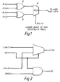
- the circuit of figure 1 may be used.
- This circuit uses eight more transistors than the XOR gate that is required if the Sum is used, but these gates are now not speed critical, and so could be substantially smaller than would previously have been the case.
- a circuit to carry out the invention may comprise two XNOR gates 12, 14 and a MUX 16. Outputs of the XNOR gates are passed to the MUX and the register value R[n-1] determines which to pass to the AND gate. Obviously this is just one means by which the function of this invention can be achieved. As will be apparent to the man skilled in the art other Boolean architectures can be chosen which have the same result.
- the second part of the new circuit takes these results a stage further by indicating what the effect of the incorrect carry value will be. This is achieved by comparing the required 'carry in" at every bit position to produce the target result with the actual carry in. If the carry required to produce the target value is a 1, but the actual carry is a 0 the result will be less than the target value. If the required carry is a 0, but the actual carry is a 1, the result will be more than the target value.
- FIG. 3 shows the basic building block for this.
- the Z and H values are used to determine if the sum A+B will be equal to K. If they are not, the value of the required carry-in at the left most failing position determines which is the larger, A+B or K
- this circuit is significantly faster than performing the addition and then passing the result to a magnitude comparator.
- the number of transistor per bit required for this circuit is constant, and the delay increases only logarithmically.
- Cinr V xor p 111011
Landscapes
- Engineering & Computer Science (AREA)
- General Physics & Mathematics (AREA)
- Physics & Mathematics (AREA)
- Theoretical Computer Science (AREA)
- Mathematical Analysis (AREA)
- Pure & Applied Mathematics (AREA)
- Computational Mathematics (AREA)
- Mathematical Optimization (AREA)
- General Engineering & Computer Science (AREA)
- Computing Systems (AREA)
- Error Detection And Correction (AREA)
- Test And Diagnosis Of Digital Computers (AREA)
- Tests Of Electronic Circuits (AREA)
- Detection And Correction Of Errors (AREA)
Applications Claiming Priority (2)
| Application Number | Priority Date | Filing Date | Title |
|---|---|---|---|
| GB9419614 | 1994-09-29 | ||
| GB9419614A GB2293665A (en) | 1994-09-29 | 1994-09-29 | A look-ahead scheme. |
Publications (3)
| Publication Number | Publication Date |
|---|---|
| EP0704793A2 true EP0704793A2 (de) | 1996-04-03 |
| EP0704793A3 EP0704793A3 (de) | 1996-05-01 |
| EP0704793B1 EP0704793B1 (de) | 2002-05-08 |
Family
ID=10762062
Family Applications (1)
| Application Number | Title | Priority Date | Filing Date |
|---|---|---|---|
| EP95306861A Expired - Lifetime EP0704793B1 (de) | 1994-09-29 | 1995-09-28 | Verfahren und Schaltungsanordnung zum Vergleichen der Summe zweier Zahlen mit einer dritten Zahl |
Country Status (5)
| Country | Link |
|---|---|
| US (1) | US5739745A (de) |
| EP (1) | EP0704793B1 (de) |
| JP (1) | JP3696669B2 (de) |
| DE (1) | DE69526618T2 (de) |
| GB (1) | GB2293665A (de) |
Families Citing this family (1)
| Publication number | Priority date | Publication date | Assignee | Title |
|---|---|---|---|---|
| KR100305679B1 (ko) * | 1999-02-24 | 2001-09-26 | 윤종용 | 반도체 메모리 장치의 테스터의 테스터 방법 및 그 장치 |
Family Cites Families (7)
| Publication number | Priority date | Publication date | Assignee | Title |
|---|---|---|---|---|
| DE191452C (de) * | ||||
| BE636282A (de) * | 1962-08-29 | 1900-01-01 | ||
| EP0191452B1 (de) * | 1985-02-11 | 1989-05-10 | Siemens Aktiengesellschaft | Verfahren und Schaltungsanordnung zur Überwachung der Summe bzw. Differenz zweier Grössen durch Vergleich mit einer dritten Grösse in binärer Darstellung |
| US4737926A (en) * | 1986-01-21 | 1988-04-12 | Intel Corporation | Optimally partitioned regenerative carry lookahead adder |
| US4924422A (en) * | 1988-02-17 | 1990-05-08 | International Business Machines Corporation | Method and apparatus for modified carry-save determination of arithmetic/logic zero results |
| US4935719A (en) * | 1989-03-31 | 1990-06-19 | Sgs-Thomson Microelectronics, Inc. | Comparator circuitry |
| US5528181A (en) * | 1994-11-02 | 1996-06-18 | Advanced Micro Devices, Inc. | Hazard-free divider circuit |
-
1994
- 1994-09-29 GB GB9419614A patent/GB2293665A/en not_active Withdrawn
-
1995
- 1995-09-28 DE DE69526618T patent/DE69526618T2/de not_active Expired - Lifetime
- 1995-09-28 EP EP95306861A patent/EP0704793B1/de not_active Expired - Lifetime
- 1995-09-28 JP JP25146595A patent/JP3696669B2/ja not_active Expired - Fee Related
-
1997
- 1997-03-04 US US08/811,333 patent/US5739745A/en not_active Expired - Lifetime
Non-Patent Citations (1)
| Title |
|---|
| None |
Also Published As
| Publication number | Publication date |
|---|---|
| DE69526618D1 (de) | 2002-06-13 |
| JP3696669B2 (ja) | 2005-09-21 |
| US5739745A (en) | 1998-04-14 |
| EP0704793B1 (de) | 2002-05-08 |
| EP0704793A3 (de) | 1996-05-01 |
| DE69526618T2 (de) | 2002-10-31 |
| JPH08185310A (ja) | 1996-07-16 |
| GB9419614D0 (en) | 1994-11-16 |
| GB2293665A (en) | 1996-04-03 |
Similar Documents
| Publication | Publication Date | Title |
|---|---|---|
| US5586069A (en) | Arithmetic logic unit with zero sum prediction | |
| US5317527A (en) | Leading one/zero bit detector for floating point operation | |
| EP0585619B1 (de) | Verfahren zur Feststellung eines nullwertigen Ergebnisses als Folge einer arithmetischen oder logischen Berechnung und Schaltung hierfür | |
| JPH0542011B2 (de) | ||
| US20130151579A1 (en) | Apparatuses and related methods for overflow detection and clamping with parallel operand processing | |
| US4618956A (en) | Method of operating enhanced alu test hardware | |
| EP0487814A2 (de) | Überlauferkennung für Drei-Operand-ALUs in einem Rechner mit skalierbarem, zusammensetzbarem Befehlssatz | |
| US4811272A (en) | Apparatus and method for an extended arithmetic logic unit for expediting selected floating point operations | |
| US6629118B1 (en) | Zero result prediction | |
| EP0539010B1 (de) | Verfahren und Anordung zur Erzeugung von Summeinformation-/Rundungskontrolle-Signal | |
| CA1173918A (en) | Cmos static alu | |
| EP0704793A2 (de) | Verbesserungen an oder in Bezug auf eine Vergleicherschaltung | |
| US5257217A (en) | Area-efficient multiplier for use in an integrated circuit | |
| US20030061253A1 (en) | Adder increment circuit | |
| US5644521A (en) | Comparator scheme | |
| EP0762268A1 (de) | Apparat und Verfahren zur Feststellung des höchstwertigen Bit | |
| JPH01304542A (ja) | パリテイ予測回路 | |
| EP0328779A2 (de) | Sprungvorhersagevorrichtung für Komputerbefehle | |
| EP0313817A2 (de) | Verfahren und Vorrichtung zur eindeutigen Schätzung von Bedingungen in einem Datenprozessor | |
| US6631393B1 (en) | Method and apparatus for speculative addition using a limited carry | |
| US5051943A (en) | Adder circuit with an encoded carry | |
| US6820109B2 (en) | System and method for predictive comparator following addition | |
| CA1127313A (en) | Fibonacci p-code parallel adder | |
| JPS61275936A (ja) | 条件決定装置 | |
| JPH03105615A (ja) | 最大値または最小値検出機能をそなえた乗算および加算複合演算回路 |
Legal Events
| Date | Code | Title | Description |
|---|---|---|---|
| PUAI | Public reference made under article 153(3) epc to a published international application that has entered the european phase |
Free format text: ORIGINAL CODE: 0009012 |
|
| PUAL | Search report despatched |
Free format text: ORIGINAL CODE: 0009013 |
|
| AK | Designated contracting states |
Kind code of ref document: A2 Designated state(s): DE FR GB IT NL |
|
| RTI1 | Title (correction) | ||
| RTI1 | Title (correction) | ||
| AK | Designated contracting states |
Kind code of ref document: A3 Designated state(s): DE FR GB IT NL |
|
| 17P | Request for examination filed |
Effective date: 19961014 |
|
| 17Q | First examination report despatched |
Effective date: 20000204 |
|
| GRAG | Despatch of communication of intention to grant |
Free format text: ORIGINAL CODE: EPIDOS AGRA |
|
| GRAG | Despatch of communication of intention to grant |
Free format text: ORIGINAL CODE: EPIDOS AGRA |
|
| GRAH | Despatch of communication of intention to grant a patent |
Free format text: ORIGINAL CODE: EPIDOS IGRA |
|
| REG | Reference to a national code |
Ref country code: GB Ref legal event code: IF02 |
|
| GRAH | Despatch of communication of intention to grant a patent |
Free format text: ORIGINAL CODE: EPIDOS IGRA |
|
| GRAA | (expected) grant |
Free format text: ORIGINAL CODE: 0009210 |
|
| AK | Designated contracting states |
Kind code of ref document: B1 Designated state(s): DE FR GB IT NL |
|
| PG25 | Lapsed in a contracting state [announced via postgrant information from national office to epo] |
Ref country code: NL Free format text: LAPSE BECAUSE OF FAILURE TO SUBMIT A TRANSLATION OF THE DESCRIPTION OR TO PAY THE FEE WITHIN THE PRESCRIBED TIME-LIMIT Effective date: 20020508 Ref country code: IT Free format text: LAPSE BECAUSE OF FAILURE TO SUBMIT A TRANSLATION OF THE DESCRIPTION OR TO PAY THE FEE WITHIN THE PRE;WARNING: LAPSES OF ITALIAN PATENTS WITH EFFECTIVE DATE BEFORE 2007 MAY HAVE OCCURRED AT ANY TIME BEFORE 2007. THE CORRECT EFFECTIVE DATE MAY BE DIFFERENT FROM THE ONE RECORDED.SCRIBED TIME-LIMIT Effective date: 20020508 |
|
| REF | Corresponds to: |
Ref document number: 69526618 Country of ref document: DE Date of ref document: 20020613 |
|
| NLV1 | Nl: lapsed or annulled due to failure to fulfill the requirements of art. 29p and 29m of the patents act | ||
| ET | Fr: translation filed | ||
| PLBE | No opposition filed within time limit |
Free format text: ORIGINAL CODE: 0009261 |
|
| STAA | Information on the status of an ep patent application or granted ep patent |
Free format text: STATUS: NO OPPOSITION FILED WITHIN TIME LIMIT |
|
| 26N | No opposition filed |
Effective date: 20030211 |
|
| PGFP | Annual fee paid to national office [announced via postgrant information from national office to epo] |
Ref country code: GB Payment date: 20100809 Year of fee payment: 16 |
|
| PGFP | Annual fee paid to national office [announced via postgrant information from national office to epo] |
Ref country code: DE Payment date: 20100930 Year of fee payment: 16 |
|
| REG | Reference to a national code |
Ref country code: FR Ref legal event code: ST Effective date: 20110531 |
|
| PG25 | Lapsed in a contracting state [announced via postgrant information from national office to epo] |
Ref country code: FR Free format text: LAPSE BECAUSE OF NON-PAYMENT OF DUE FEES Effective date: 20100930 |
|
| PGFP | Annual fee paid to national office [announced via postgrant information from national office to epo] |
Ref country code: FR Payment date: 20090916 Year of fee payment: 15 |
|
| GBPC | Gb: european patent ceased through non-payment of renewal fee |
Effective date: 20110928 |
|
| REG | Reference to a national code |
Ref country code: DE Ref legal event code: R119 Ref document number: 69526618 Country of ref document: DE Effective date: 20120403 |
|
| PG25 | Lapsed in a contracting state [announced via postgrant information from national office to epo] |
Ref country code: DE Free format text: LAPSE BECAUSE OF NON-PAYMENT OF DUE FEES Effective date: 20120403 |
|
| PG25 | Lapsed in a contracting state [announced via postgrant information from national office to epo] |
Ref country code: GB Free format text: LAPSE BECAUSE OF NON-PAYMENT OF DUE FEES Effective date: 20110928 |