EP0695048A2 - Adaptive equalizer for analog optical signal transmission - Google Patents
Adaptive equalizer for analog optical signal transmission Download PDFInfo
- Publication number
- EP0695048A2 EP0695048A2 EP95304878A EP95304878A EP0695048A2 EP 0695048 A2 EP0695048 A2 EP 0695048A2 EP 95304878 A EP95304878 A EP 95304878A EP 95304878 A EP95304878 A EP 95304878A EP 0695048 A2 EP0695048 A2 EP 0695048A2
- Authority
- EP
- European Patent Office
- Prior art keywords
- signal
- phase
- amplitude
- electrical signal
- harmonic distortion
- Prior art date
- Legal status (The legal status is an assumption and is not a legal conclusion. Google has not performed a legal analysis and makes no representation as to the accuracy of the status listed.)
- Withdrawn
Links
- 230000003287 optical effect Effects 0.000 title claims abstract description 100
- 230000003044 adaptive effect Effects 0.000 title claims abstract description 22
- 230000008054 signal transmission Effects 0.000 title 1
- 238000012937 correction Methods 0.000 claims abstract description 85
- 230000010363 phase shift Effects 0.000 claims abstract description 16
- 230000004044 response Effects 0.000 claims abstract description 14
- 239000013598 vector Substances 0.000 claims description 14
- 238000000034 method Methods 0.000 claims description 8
- 230000003321 amplification Effects 0.000 claims description 4
- 238000003199 nucleic acid amplification method Methods 0.000 claims description 4
- 238000010586 diagram Methods 0.000 description 16
- 238000004891 communication Methods 0.000 description 10
- 230000000694 effects Effects 0.000 description 4
- 239000003990 capacitor Substances 0.000 description 3
- 239000000835 fiber Substances 0.000 description 2
- 238000004458 analytical method Methods 0.000 description 1
- 230000005540 biological transmission Effects 0.000 description 1
- 230000001413 cellular effect Effects 0.000 description 1
- 238000006243 chemical reaction Methods 0.000 description 1
- 230000001419 dependent effect Effects 0.000 description 1
- 238000010295 mobile communication Methods 0.000 description 1
- 230000004048 modification Effects 0.000 description 1
- 238000012986 modification Methods 0.000 description 1
- 239000013307 optical fiber Substances 0.000 description 1
- 230000008569 process Effects 0.000 description 1
- 238000012545 processing Methods 0.000 description 1
- 238000010223 real-time analysis Methods 0.000 description 1
Images


Classifications
-
- H—ELECTRICITY
- H04—ELECTRIC COMMUNICATION TECHNIQUE
- H04B—TRANSMISSION
- H04B10/00—Transmission systems employing electromagnetic waves other than radio-waves, e.g. infrared, visible or ultraviolet light, or employing corpuscular radiation, e.g. quantum communication
- H04B10/25—Arrangements specific to fibre transmission
- H04B10/2507—Arrangements specific to fibre transmission for the reduction or elimination of distortion or dispersion
-
- H—ELECTRICITY
- H04—ELECTRIC COMMUNICATION TECHNIQUE
- H04B—TRANSMISSION
- H04B10/00—Transmission systems employing electromagnetic waves other than radio-waves, e.g. infrared, visible or ultraviolet light, or employing corpuscular radiation, e.g. quantum communication
Definitions
- the present invention relates generally to converting electrical signals to optical signals, and more particularly to adaptively equalizing (i.e., nulling) any intermodulation distortion effects resulting from such conversion of electrical signals to optical signals.
- Data transmission over an optical communication medium is typically achieved by first converting a data signal to a modulating signal.
- Both the data signal and the modulating signal are analog RF (radio frequency) modulated electrical signals.
- the modulating signal is applied to a laser to produce a modulated optical signal such that the optical signal is an optical representation of the electrical data signal.
- the optical signal is modulated using the modulating signal such that the optical signal is embedded with the information contained in the data signal. This optical signal is then transmitted to appropriate destinations via the optical communication medium.
- the modulation response of a laser when an analog or digital RF modulating signal is applied is not linear.
- Such nonlinear modulation response characteristics result in the generation of intermodulation distortion on the transmitted signal.
- the intermodulation distortion degrades the quality and fidelity of the optical signal to be transmitted and also limits the span of optical fiber over which the signal may be transmitted.
- a prior solution to this problem involves the use of a tuned hybrid circuit to compensate for a laser's non-linearity modulation response pattern.
- This tuned hybrid circuit generates a first signal and a second signal, where the first signal has a first frequency, a first phase, and a first amplitude, and the second signal has a second frequency, a second phase, and a second amplitude.
- a human operator analyzes the intermodulation distortion products and then implements the tuned hybrid circuit using appropriate passive components (such as capacitors and resistors) so as to set the values of the first and second frequencies, phases, and amplitudes.
- appropriate passive components such as capacitors and resistors
- the first and second frequencies, phases, and amplitudes are set by the human operator so that the first and second signals are equal in amplitude but opposite in phase to the intermodulation distortion products.
- the first and second signals are used to produce the electrical modulating signal such that the optical signal produced by the laser in accordance with the electrical modulating signal does not contain any intermodulation distortion products.
- an adaptive equalizer which, without any human intervention, automatically nulls intermodulation distortion products generated as a result of a laser's non-linear modulation response pattern, and which automatically compensates for phase and/or amplitude changes in the intermodulation distortion products caused by drifting of the laser's modulation response pattern.
- the present invention is directed to an adaptive equalizer (also called a laser interface) for generating an electrical modulating signal for use by a laser to modulate an optical data signal.
- the laser has a non-linear modulation response pattern such that the optical data signal comprises a primary data signal and a plurality of harmonic distortion products.
- the adaptive equalizer operates by generating a correction electrical signal having a frequency equal to a frequency of one of the harmonic distortion products (this harmonic distortion product is nulled by operation of the adaptive equalizer).
- the adaptive equalizer detects the phase and amplitude of the harmonic distortion product. Then, the adaptive equalizer phase shifts the correction electrical signal in accordance with the detected phase such that the correction electrical signal and the harmonic distortion product are conjugately matched.
- the adaptive equalizer amplifies the phase shifted correction electrical signal in accordance with the detected amplitude such that the phase shifted correction electrical signal and the harmonic distortion product are equal in amplitude. Then, the amplified and phase shifted correction electrical signal is combined with an electrical data signal to form the electrical modulating signal.
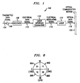
- FIG. 1 is a block diagram of a communication system 102 (only those portions of the communication system 102 relevant to the present invention are shown).
- the communication system 102 includes an antenna 106 which receives a transmitted data signal 104 that was transmitted (i.e., broadcasted) over the air by a mobile communication terminal (such as a cellular telephone, not shown).
- a mobile communication terminal such as a cellular telephone, not shown.
- the transmitted data signal 104 represents digital data or analog that is being carried by an RF (radio frequency) carrier.
- RF radio frequency
- a receiver 108 processes the transmitted data signal 104 in a well known manner to produce a preferably RF electrical data signal 110.
- the electrical data signal 110 is an electrical representation of the transmitted data signal 104. In other words, the electrical data signal 110 contains the data embedded in the transmitted data signal 104.
- a laser interface 112 converts the electrical data signal to a preferably RF electrical modulating signal 114.
- This electrical modulating signal 114 is transferred to a well known laser 116.
- the laser 116 uses the electrical modulating signal 114 in a well known manner to modulate an optical data signal 118 such that the optical data signal 118 is an optical representation of the electrical data signal 110.
- the optical data signal 118 contains the information embedded in the electrical data signal 110.
- the optical data signal 118 is transmitted to appropriate destinations via an optical communication medium 120, such as a fiber optic cable.
- the present invention is adapted for use in wireless communication applications.
- the receiver 108 is shown in FIG. 1 as being connected to the antenna 106.
- the present invention particularly the laser interface 112 may also be used in non-wireless communication applications.
- the laser interface 112 could be used when the data signal originates from a source or transmitter.
- the modulation response of the laser 116 is not linear. Consequently, the laser 116 may generate intermodulation distortion products when using the electrical modulating signal 114 to modulate the optical data signal 118. Such intermodulation distortion products are present in the optical data signal 118, and operate to compromise and distort the optical data signal 118.
- the laser interface 112 generates the electrical modulating signal 114 so as to compensate for any non-linear modulation response characteristics of the laser 116.
- the laser interface 112 identifies and quantifies any intermodulation distortion products contained in the optical data signal 118, and generates a plurality of signals which are herein called correction signals or terms 206, 208.
- correction signals 206, 208 each has a frequency, amplitude, and phase necessary to cancel the intermodulation distortion products when combined with the electrical modulating signal.
- the laser interface 112 uses the correction signals 206, 208 to generate the electrical modulating signal 114, such that the laser 116 does not generate intermodulation distortion products when using the electrical modulating signal 114 to modulate the optical data signal 118.
- the laser interface 112 automatically performs such cancellation (nulling) of the intermodulation distortion products generated by the laser 116. No human intervention is necessary. In particular, it is not necessary for a human operator to manually determine and set the frequency, phase, and/or amplitude of the correction signals 206, 208. Instead, the correction signals 206, 208 are automatically generated.
- the laser interface 112 automatically compensates for any phase and/or amplitude changes in the intermodulation distortion products caused by drifting of the modulation response pattern of the laser 116.
- the laser interface 112 automatically adjusts the phase and/or amplitude of the correction signals 206, 208 to compensate for any changes in the phase and/or amplitude of the intermodulation distortion products generated by the laser 116.
- the laser interface 112 of the present invention is described in detail in the following sections.
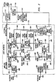
- FIG. 2 is a block diagram of the laser interface 112 according to a preferred embodiment of the present invention.
- FIG. 2 also shows, in block diagram form, details of the well known laser 116 which are pertinent to the present invention.
- the laser 116 includes an electrical-to-optical converter 210 which, in a well known manner, uses the electrical modulating signal 114 (generated by the laser interface 112) to modulate the optical data signal 118 such that the optical data signal 118 is an optical representation of the electrical data signal 110.
- the optical data signal 118 is transmitted to appropriate destinations via an optical communication medium 120 (FIG. 1).
- the optical data signal 118 is also provided to an optical detector 212.
- the optical detector 212 operates in a well known manner to convert the optical data signal 118 to an electrical signal 214, called the "detected signal" in FIG. 2.
- the detected signal 214 is an electrical representation of the optical data signal 118 including any intermodulation distortion products present in the optical data signal 118. As such, any intermodulation distortion products contained in the optical data signal 118 are electrically represented in the detected signal 214.
- the structure and operation of the electrical-to-optical converter 210 and the optical detector will be apparent to persons skilled in the relevant art.
- the optical data signal 118 generated by the laser 116 includes a primary signal and a number of harmonics.
- the primary signal represents the "pure" optical representation of the electrical data signal 110. For example, if the electrical data signal 110 is sin(wt), then the primary signal of the optical data signal 118 is also sin(wt).
- the harmonics of the optical data signal 118 represent the intermodulation distortion effects.
- Such harmonics include a second order harmonic, a third order harmonic, a fourth order harmonic, etc. (These are called, simply, the second harmonic, the third harmonic, etc.) If the electrical data signal 110 is sin(wt), then the second harmonic is sin(2wt), the third harmonic is sin(3wt), etc., as described by the Fourier harmonic series.
- the laser interface 112 includes a linear signal amplifier 202 which amplifies the electrical data signal 110 to produce an amplified data signal 204. Such amplification is necessary to compensate for any losses incurred from prior processing of the electrical data signal 110 by the antenna 106 and/or the receiver 108 (FIG. 1).
- the structure and operation of the linear signal amplifier 202 will be apparent to persons skilled in the relevant art.
- the laser interface 112 also includes a number of components which operate to generate a second harmonic correction term 206 and a third harmonic correction term 208.
- the amplified data signal 204 is combined in a well known manner with the second harmonic correction term 206 and the third harmonic correction term 208 to produce the electrical modulating signal 114 (for example, power representative of the amplified data signal 204, the second harmonic correction term 206, and the third harmonic correction term 208 may be summed).
- the second harmonic correction term 206 has the same frequency and amplitude as the second harmonic of the optical data signal 118.
- the second harmonic correction term 206 and the second harmonic of the optical data signal 118 are conjugately matched with one another (conjugate matching of two sin waves is well known and well documented and states that the mathematical relationship between two conjugately matched sine waves is such that when they are added together they cancel, or null, each other). In the simplest case they would be of the same frequency and amplitude, but with conjugate (i.e., 180° out of phase) phase.
- conjugate i.e. 180° out of phase
- the second harmonic correction term 206 operates to equalize the effects of the second harmonic of the optical data signal 118.
- the second harmonic correction term 206 operates to cancel (or null) the second harmonic of the optical data signal 118. More particularly, by using the second harmonic correction term 206 to produce the electrical modulating signal 114, the electrical modulating signal 114 is adjusted (relative to the immediately preceding version of the electrical modulating signal 114) so that the laser 116 does not produce the second harmonic when using the electrical modulating signal 114 to modulate the optical data signal 118.
- the third harmonic correction term 208 has the same frequency and amplitude as the third harmonic of the optical data signal 118, and is conjugately matched with the third harmonic of the optical data signal 118. Accordingly, the third harmonic correction term 208 operates to equalize the effects of the third harmonic of the optical data signal 118. In other words, the third harmonic correction term 208 operates to cancel (or null) the third harmonic of the optical data signal 118. More particularly, by using the third harmonic correction term 208 to produce the electrical modulating signal 114, the electrical modulating signal 114 is adjusted (relative to the immediately preceding version of the electrical modulating signal 114) so that the laser 116 does not produce the third harmonic when using the electrical modulating signal 114 to modulate the optical data signal 118.
- the laser interface 112 cancels out only the second and third harmonics of the optical data signal 118. This is the case, since the second and third harmonics represent the intermodulation distortion products having the greatest impact on the optical data signal 118. In alternate embodiments of the invention, however, the laser interface 112 cancels out additional harmonics of the optical data signal 118. In such alternate embodiments, the laser interface 112 generates correction terms other than the second harmonic correction term 206 and the third harmonic correction term 208. Modification of the laser interface 112 to generate such additional correction terms will be apparent to persons skilled in the relevant art based on the discussion contained herein.
- FIG. 3 is a flowchart 302 depicting the operation of the laser interface 112.
- the linear signal amplifier 202 in the laser interface 112 amplifies the electrical data signal 110 to produce the amplified data signal 204.
- This amplified data signal 204 is combined with the second harmonic correction term 206 and the third harmonic correction term 208 to produce the electrical modulating signal 114.
- a first voltage controlled oscillator (VCO) 232 generates a signal 236 (called herein the first signal for reference purposes) having the same frequency as the second harmonic of the optical data signal 118.
- a second VCO 234 generates a signal 238 (called herein the second signal for reference purposes) having the same frequency as the third harmonic of the optical data signal 118.
- the first and second VCOs 232, 234 generate the first and second signals 236, 238 at such frequencies in accordance with frequency tuning control signals 230 generated by a frequency tuning control 228.
- the first and second signals 236, 238 could be produced by an auxiliary signal generator.
- the first VCO 232 operates such that the first signal 236 comprises two balanced signals of equal amplitude and having a phase difference of 90 degrees.
- a balanced signal comprises two identical signals that have a phase difference of 180 degrees (they are the inverse of one another).
- the second VCO 234 operates such that the second signal 238 comprises two balanced signals of equal amplitude and having a phase difference of 90 degrees.
- the first and second VCOs 232, 234 are described in a Patent Application entitled "A Modem Having a Phase Corrector and a Voltage Controlled Oscillator Implemented Using A Multi-Stage Ring Oscillator", claiming priority from U.S. patent application 08/280 638 of 25.7.94.
- an error signal detector 216 in the laser interface 112 receives the detected signal 214 that was generated by the optical detector 212 in the laser 116.
- the detected signal 214 is an electrical representation of the optical data signal 118.
- the detector 218 can reside external to the laser 116.
- the error signal detector 216 identifies and quantifies the intermodulation distortion products contained in the detected signal 214 (step 314). Specifically, the error signal detector 216 determines the phase and the amplitude of preferably the second and third harmonics contained in the optical data signal 118 (as electrically represented in the detected signal 214). Such phase information and amplitude information for the second and third harmonics are encapsulated in an error signal 218, which is provided to a vector modulation controller 220.
- the vector modulation controller 220 uses the error signal 218 to generate phase control signals 252, 254 and amplitude control signals 256, 258.
- the phase control signal 252 indicates the degree to which the phase of the first signal 236 must be modified so that the first signal 236 is conjugately matched with the second harmonic of the optical data signal 118.
- the phase control signal 254 indicates the degree to which the phase of the second signal 238 must be modified so that the second signal 238 is conjugately matched with the third harmonic of the optical data signal 118.
- the amplitude control signal 256 indicates the degree to which the amplitude of the first signal 236 must be modified so that the first signal 236 has the same amplitude as the second harmonic of the optical data signal 118.
- the amplitude control signal 258 indicates the degree to which the amplitude of the second signal 238 must be modified so that the second signal 238 has the same amplitude as the third harmonic of the optical data signal 118.
- the phase control signal 252 is provided to a first RF phase modulator 240.
- the first RF phase modulator 240 generates, in accordance with the phase control signal 252, a phase shifted first signal 244 from the first signal 236, wherein the phase shifted first signal 244 is conjugately matched to the appropriate distortion product (the second harmonic in this case) of the optical data signal 118.
- the amplitude control signal 256 is provided to a first RF amplitude modulator 248.
- the first RF amplitude modulator 248 generates, in accordance with the amplitude control signal 256, a second harmonic correction term 206 from the phase shifted first signal 244, wherein the amplitude of the second harmonic correction term 206 is such as to null out the second harmonic of the optical data signal 118.
- the frequency of the second harmonic correction term 206 is such as to null out the second harmonic of the optical data signal 118.
- the phase shifted first signal 244 is conjugately matched to the second harmonic of the optical data signal 118. Conjugate matching of the first signal 244 with the appropriate distortion product in the optical data signal 118 will cancel (or null) the distortion in the optical data signal 118.
- a second phase control signal 254 is provided to a second RF phase modulator 242.
- the second RF phase modulator 242 generates, in accordance with the phase control signal 254, a phase shifted second signal 246 from the second signal 238, wherein the phase shifted second signal 246 is conjugately matched to the third harmonic of the optical data signal 118.
- the amplitude control signal 258 is provided to a second RF amplitude modulator 250.
- the second RF amplitude modulator 250 generates, in accordance with the amplitude control signal 258, a third harmonic correction term 208 from the phase shifted second signal 246, wherein the amplitude of the third harmonic correction term 208 is such as to null out the third harmonic of the optical data signal 118.
- the frequency of the third harmonic correction term 208 is such as to null out the third harmonic of the optical data signal 118.
- the phase shifted second signal 246 is conjugately matched to the third harmonic of the optical data signal 118. Conjugate matching of the second signal 246 with the appropriate distortion product in the optical data signal 118 will cancel (or null) the distortion in the optical data signal 118.
- the second harmonic correction term 206 and the third harmonic correction term 208 are combined with the amplified data signal 204 to produce the electrical modulating signal 114, as discussed above (step 308).
- the present invention automatically cancels (without any human intervention) any intermodulation distortion products generated by the laser 116 when using the electrical modulating signal 114 to modulate the optical data signal 118.
- Such automatic cancellation of intermodulation distortion products is achieved by producing the electrical modulating signal 114 using correction term signals (i.e., the second harmonic correction term 206 and the third harmonic correction term 208) which are conjugately matched and thus have an appropriate frequency, amplitude, and phase with respect to the intermodulation distortion products so as to exactly cancel the intermodulation distortion products, and by automatically and continuously generating such correction term signals 206, 208 based on a real-time analysis of the detected signal 214 (which is an electrical representation of the optical data signal 118).
- correction term signals i.e., the second harmonic correction term 206 and the third harmonic correction term 208
- the present invention automatically adjusts to changes in the frequency, amplitude and phase of the intermodulation distortion products (caused by drifting of the modulation response pattern of the laser 116).
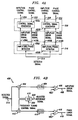
- FIG. 4A is a block diagram of the error signal detector 216 and the vector modulation controller 220.
- the error signal detector 216 is considered in this section and the vector modulation controller 220 is considered in the next section.
- the error signal detector 216 includes an amplitude/phase detector 430 for each harmonic of the optical data signal 118 that is being nulled. Thus, since preferably the second and the third harmonics are being nulled, the error signal detector 216 includes two amplitude/phase detectors 430A, 430B. Each of the amplitude/phase detectors 430 receives the detected signal 214 (generated by the optical detector 212 in the laser 116, FIG. 2) and generates an amplitude error signal 408 and a phase error signal 418.
- FIG. 4B is a more detailed block diagram of the amplitude/phase detectors 430.
- Each amplitude/phase detector 430 includes a voltage controlled oscillator 410 which generates a signal having a frequency appropriate to cancel the harmonic in question.
- the VCO 410 in the amplitude/phase detector 430A associated with the second harmonic of the optical data signal 118 generates a signal having a frequency equal to the frequency of the second harmonic.
- the VCO 410 is phase locked to the electrical data signal 110 (FIG. 1), such that the signal generated by the VCO 410 has the same phase as the electrical data signal 110.
- an external reference selector 224 which is a well known frequency divider (also called a prescaler), generates an adjusted reference signal 223 from a reference signal 222. This reference signal 222 has the same phase as the electrical data signal 110.
- the signal generated by the VCO 410 includes a sine component and a cosine component.
- the detected signal 214 may be represented a sine wave.
- the sine component of the signal produced by the VCO 410 is combined with the detected signal 214 in a well known mixer 402.
- the structure and operation of the mixer 402 will be apparent to persons skilled in the relevant art.
- the output of this mixer 402 is a DC voltage having a magnitude proportional to the magnitude of the harmonic in question.
- the output of the mixer 402 in the amplitude/phase detector 430A associated with the second harmonic of the optical data signal 118 is a DC voltage having a magnitude substantially equal to the magnitude of the second harmonic.
- the DC voltage output from the mixer 402 is applied to a well known filter 404 which operates in a well known manner to filter out any remaining AC components from the DC voltage.
- the filter 404 comprises a switched capacitor filter which operates to remove excess noise and spurious RF signals from the true error signal.
- the filtered DC voltage output from the filter 404 is applied to a voltage comparator 406.
- the voltage comparator 406 operates in a well known manner to compare this filtered DC voltage to a reference voltage Vref.
- the comparator 406 functions as a well known slice amplifier and level comparator to provide discrete error signal levels of the appropriate voltage to allow the modulation controller 220 to function properly.
- the cosine component of the signal produced by the VCO 410 is combined with the detected signal 214 in a well known mixer 412.
- the structure and operation of the mixer 412 will be apparent to persons skilled in the relevant art.
- the output of this mixer 412 is a DC voltage having a magnitude proportional to the phase of the harmonic distortion term in the optical signal 118.
- the output of the mixer 412 in the amplitude/phase detector 430A associated with the second harmonic of the optical data signal 118 is a DC voltage having a magnitude proportional to the phase of the second harmonic.
- the DC voltage output from the mixer 412 is applied to a well known filter 414 which operates in a well known manner to filter out any remaining AC components from the DC voltage.
- the filter 414 includes a switched capacitor low-pass filter which operates to remove excess noise and spurious RF signals from the true error signal.
- the filtered DC voltage output from the filter 414 is applied to a voltage comparator 416.
- the voltage comparator 416 operates in a well known manner to compare this filtered DC voltage to a reference voltage Vref'.
- the voltage comparator 416 in a well known manner, outputs a voltage signal, called the phase error signal 418, having one of a discrete number of logic levels (preferably, between five to ten discrete logic levels are used) closest to the magnitude of the filtered DC voltage output from the filter 414.
- the comparator 416 functions as a well known slice amplifier and level comparator to provide discrete error signal levels of the appropriate voltage to allow the modulation controller 220 to function properly.
- the vector modulation controller 220 includes a control signal generator 432 for each harmonic of the optical data signal 118 that is being nulled.
- the vector modulation controller 220 includes two control signal generators 432A, 432B.
- Each of the control signal generators 432 receives the amplitude error signal 408 and the phase error signal 418 from the corresponding amplitude/phase detector 430 in the error signal detector 216, and generates an amplitude control signal 256 and a phase control signal 252.
- FIG. 5 is a block diagram of the control signal generators 432.
- Each control signal generator 432 includes a buffer 502 which receives the respective amplitude error signal 408.
- the buffer 502 is a well known sample and hold amplifier, and operates to store the voltage that is present at its input (i.e., the amplitude error signal 408).
- the stored amplitude error signal 408 is output from the buffer 502 as a VAGC signal 506 (VAGC stands for voltage amplifier gain control).
- VAGC voltage amplifier gain control
- the buffer 502 also outputs a VAGCB signal 508 (the "B” stands for "bar”, i.e., "inverse"), which is identical to the VAGC signal 506 except that it has opposite phase (i.e., the VAGC signal 506 and the VAGCB signal 508 are 180 degrees out of phase).
- the manner in which the VAGCB signal 508 may be generated from the VAGC signal 506 will be apparent to persons skilled in the relevant art.
- the VAGC signal 506 and the VAGCB signal 508 collectively represent the amplitude control signal 256 or 258.
- Each control signal generator 432 also includes a digital signal processor (DSP) 504 which receives the respective phase error signal 418.
- the DSP 504 analyzes the phase error signal 418 and determines the phase shift that is necessary to make the respective correction term 206 or 208 cancel the harmonic in question.
- the DSP 504 in the control signal generator 432A associated with the second harmonic analyzes the phase error signal 418A and determines the phase shift that is necessary to make the second harmonic correction term 206 cancel the second harmonic of the optical data signal 118.
- the DSP 504 represents this phase shift by appropriately outputing an A voltage 510, a B digital value 512, and a C digital value 514.
- the B digital value 512 is set to 1 and the C digital value 514 is set to 1.
- the B and C digital values 512, 514 are set to "01", "10", or "00", respectively.
- the A voltage 510 determines the exact phase shift within a range. For example, if the B and C digital values 512, 514 are set to "01" such that the phase shift is within the range from 90 to 180 degrees, the A voltage 510 indicates the exact phase shift within the range (whether the phase shift is 91 degrees, 92 degrees, etc.).
- the DSP 504 operates as follows to generate the A voltage 510, the B digital value 512, and the C digital value 514.
- the DSP 504 operates as a programmable digital logic element which provides the control signals to operate the phase shifter elements within the integrated circuit (IC).
- the DSP 504 functions as an 4-bit magnitude comparator with an input buffer amplifier and a digital and carry output.
- the magnitude of the phase error signal 418 at the appropriate frequency is buffered to adjust the input voltage range to a necessary level for the magnitude comparator to operate correctly.
- the comparator then generates a successive approximation of the magnitude of the input phase error signal 418 and enables a digital latch buffer connected to lines 512, 514, 518, and 520.
- the latched output from the comparator provides a digital output control in lines 512, 514, 518, and 520.
- the magnitude of the carry output is again buffered to provide an appropriate voltage level control signal on lines 510 and 516.
- the DSP 504 contains monitor taps so that the voltage value of all control lines can be monitored and the DSP 504 can also be reset by applying an external strobe input to the DSP 504.
- the DSP 504 also outputs AB, BB, and CB signals 516, 518, 520, which are identical to but opposite in phase to the A, B, and C signals 510, 512, 514, respectively.
- the manner in which the AB, BB, and CB signals 516, 518, 520 may be generated from the A, B, and C signals 510, 512, 514 will be apparent to persons skilled in the relevant art.
- the A, B, and C signals 510, 512, 514 and the AB, BB, and CB signals 516, 518, 520 collectively represent the phase control signal 252 or 254.
- FIG. 6 is a circuit diagram of the first RF phase modulator 240 according to a preferred embodiment of the present invention.
- the structure and operation of the second RF phase modulator 242 is identical to that of the first RF phase modulator 240. Therefore, the circuit diagram shown in FIG. 6, as well as the following discussion, apply equally well to the second RF phase modulator 242.
- the A, B, and C signals 510, 512, 514 and the AB, BB, and CB signals 516, 518, 520 generated by the DSP 504 in the control signal generator 432A in the vector modulation controller 220 are applied to the bases of transistors Q3, Q5, Q6, Q21, Q19, and Q18, respectively.
- the first signal 236 generated by the first VCO 232 is applied to the base of transistor Q1.
- a first signal bar 602 which is identical to the first signal 236 except opposite in phase (180 degree phase difference), is applied to the base of transistor Q2. The manner in which the first signal bar 602 may be generated from the first signal 236 will be apparent to persons skilled in the relevant art.
- the first signal 236 and the first signal bar 602 represent the first balanced signal generated by the first VCO 232.
- the second balanced signal generated by the first VCO 232 which is equal in magnitude but 90 degrees out of phase with the first balanced signal, is represented by a V90 signal and a V90B signal.
- the V90 signal is applied to the base of transistor Q23 and the V90B signal is applied to the base of transistor Q22.
- the first RF phase modulator 240 operates to shift the phase of the first signal 236 by an amount designated by the A, B, and C signals 510, 512, and 514. For example, as discussed above, if the B and C digital values 512, 514 are equal to "01", then the phase of the first signal 236 is shifted from 90 to 180 degrees. The A voltage 510 indicates the exact phase shift within this range of 90 to 180 degrees.
- the first RF modulator 240 generates a balanced output voltage signal VO/VOB, which represents the first signal 236 after its phase has been shifted as discussed above.
- the frequency of the balanced output voltage signal VO/VOB is equal to the frequency of the first signal 236.
- the signals VO and VOB are 180 degrees out of phase.
- the balanced output voltage signal VO/VOB is provided as the phase shifted first signal 244 to the first RF amplitude modulator 248 (in other words, the balanced output voltage signal VO/VOB and the phase shifted first signal 244 are the same).
- the phase shifted first signal 704 is equal to VO and the phase shifted first signal (bar) 702 is equal to VOB (see Fig. 7).
- the first RF phase modulator 240 operates to generate the output voltage signal VO as follows.
- the first RF phase modulator 240 provides a phase shift between 0 and 360 degrees.
- the actual phase shift is achieved by taking a linear combination of the basis vector signals which are equivalent to the first and second signals generated by the first VCO 232.
- the phase difference between the first and second balanced signals of VCO 232 equals 90 degrees. Therefore, the two balanced signals are orthogonal and by taking a linear combination of the two balanced vectors by adjusting the control signals 510, 512, 514, 516, 518, and 520, the phase at the output VO/VOB may be varied continuously over the full 360 degree cycle.
- the output balanced signal VO/VOB will have constant amplitude over the full 360 degree phase space.
- the above also describes the operation of the second RF phase modulator 242. Further details- pertaining to the first RF phase modulator 240 will be apparent to persons skilled in the relevant art based on the teachings contained herein.
- FIG. 7 is a circuit diagram of the first RF amplitude modulator 248 according to a preferred embodiment of the present invention.
- the structure and operation of the second RF amplitude modulator 250 is identical to that of the first RF amplitude modulator 248. Therefore, the circuit diagram shown in FIG. 7, as well as the following discussion, apply equally well to the second RF amplitude modulator 250.
- the first RF amplitude modulator 248 includes a predistortion stage 710 and an amplifier stage 712.
- the VAGC signal 506 and the VAGCB signal 508 from the buffer 502 in the control signal generator 432A of the error signal detector 216 are applied to the bases of transistors T2 and T5, respectively, in the predistortion stage 710.
- the phase shifted first signal 244 and the phase shifted first signal (bar) 702 are applied to the bases of transistors T13 and T9, respectively, in the amplifier stage 712.
- the predistortion stage 710 operates in a well known manner to enable linear control of the gain of the amplifier stage 712.
- the predistortion stage 710 operates to generate a gain control voltage 714 that is applied to the bases of transistors T7 and T12 and gain control voltage (bar) 716 that is applied to the bases of transistors T8 and T11.
- the manner in which this balanced gain control voltage 714/716 is generated is as follows.
- Voltages VAGC and VAGCB represent a balanced voltage VAGC'. This balanced voltage VAGC' is applied at the bases of transistors T2 and T5 which represent an emitter coupled pair. For most cases resistor RE1 is used to linearize the operation of T2 and T5.
- This emitter coupled pair converts the voltage VAGC' into a differential current present at the collectors of T2 and T5. This current next generates a differential logarithmic voltage across transistors T1 and T4. This voltage is then applied to the bases of transistors T7, T8, and T12, T11 each representing emitter coupled pairs. As will be appreciated by persons skilled in the relevant art, when the logarithmic voltage is applied in this fashion to the bases of the emitter coupled pairs, the gain of the amplifier stage 712 is linearized with respect to VAGC'.
- the amplifier stage 712 operates to amplify the phase shifted first signal 244 to thereby generate an output voltage signal Vout that has an amplitude appropriate to cancel the second harmonic of signal 118.
- the output voltage signal Vout has the appropriate frequency as the second harmonic, and is of appropriate phase to cancel the second harmonic of signal 118.
- the output voltage signal Vout represents the second harmonic correction term 206 (FIG. 2), which is used to produce the electrical modulating signal 114.
- the amplifier stage 712 functions as a variable gain stage where the voltage gain depends on the VAGC' voltage. If the VAGC' voltage (506-508) is increased, more current flows in the collectors of transistors T8 and T11 as compared to transistors T7 and T12. This causes the amplifier gain to decrease since now more of the current of collectors T9 and T13 is steered to transistors T8 and T11 (away from loads RE2 and RE3) which are loaded by a short to VCC. Transistors T7 and T8, T11 and T12 are used as a steering switch to direct current toward and away from RE2 and RE3, thereby adjusting the voltage gain of the amplifier stage 712. The above also applies to the second RF amplitude modulator 250.
- the gain of the amplifier stage 712 ranges from 0 (if the magnitude of VAGC 506 is high) to 2*RE2*(amplitude of the phase shifted first signal 244)/RE4 (if the magnitude of VAGC 506 is low).
- RE2 and RE3 are each equal to 100 ohms and RE4 is equal to 25 ohms. However, these values are implementation dependent.
- the RF amplitude modulator 248 can be cascaded with other amplitude modulators if necessary to achieve the desired amplification/attenuation.
- the manner in which the laser interface 112 can be modified to include cascaded RF amplitude modulators will be apparent to persons skilled in the art based on the discussion contained herein.
Landscapes
- Physics & Mathematics (AREA)
- Electromagnetism (AREA)
- Engineering & Computer Science (AREA)
- Computer Networks & Wireless Communication (AREA)
- Signal Processing (AREA)
- Optical Communication System (AREA)
Applications Claiming Priority (2)
| Application Number | Priority Date | Filing Date | Title |
|---|---|---|---|
| US08/280,639 US5473460A (en) | 1994-07-25 | 1994-07-25 | Adaptive equalizer for analog optical signal transmission |
| US280639 | 2002-10-24 |
Publications (1)
| Publication Number | Publication Date |
|---|---|
| EP0695048A2 true EP0695048A2 (en) | 1996-01-31 |
Family
ID=23073969
Family Applications (1)
| Application Number | Title | Priority Date | Filing Date |
|---|---|---|---|
| EP95304878A Withdrawn EP0695048A2 (en) | 1994-07-25 | 1995-07-12 | Adaptive equalizer for analog optical signal transmission |
Country Status (5)
| Country | Link |
|---|---|
| US (1) | US5473460A (ko) |
| EP (1) | EP0695048A2 (ko) |
| JP (1) | JP3429395B2 (ko) |
| KR (1) | KR100325573B1 (ko) |
| TW (1) | TW260783B (ko) |
Families Citing this family (13)
| Publication number | Priority date | Publication date | Assignee | Title |
|---|---|---|---|---|
| US5710653A (en) * | 1995-03-06 | 1998-01-20 | Fiber Optic Network Solutions Corp. | Linear multi-output optical transmitter system |
| IL118873A0 (en) * | 1996-07-16 | 1996-10-31 | I R Lan Ltd | Optical detector system and optical communication apparatus including same |
| WO2002062221A1 (en) * | 2001-02-07 | 2002-08-15 | East Carolina University | Hearing assessment via computer network |
| US7003228B2 (en) * | 2001-09-11 | 2006-02-21 | Vitesse Semiconductor Corporation | Method and apparatus for improved high-speed adaptive equalization |
| US7466925B2 (en) * | 2004-03-19 | 2008-12-16 | Emcore Corporation | Directly modulated laser optical transmission system |
| JP2005317666A (ja) * | 2004-04-27 | 2005-11-10 | Sumitomo Electric Ind Ltd | レーザ駆動回路 |
| US8792640B2 (en) | 2008-01-29 | 2014-07-29 | Sony Corporation | Systems and methods for securing a digital communications link |
| US10368785B2 (en) | 2008-10-24 | 2019-08-06 | East Carolina University | In-ear hearing test probe devices and methods and systems using same |
| WO2011006051A1 (en) * | 2009-07-09 | 2011-01-13 | Georgia Tech Research Corporation | Systems and methods for providing physical layer security |
| US8855175B2 (en) | 2012-08-02 | 2014-10-07 | Telefonaktiebolaget L M Ericsson (Publ) | Low complexity all-digital PIM compensator |
| US8890619B2 (en) | 2012-08-02 | 2014-11-18 | Telefonaktiebolaget L M Ericsson (Publ) | PIM compensation in a receiver |
| US9184652B2 (en) * | 2012-08-28 | 2015-11-10 | Enphase Energy, Inc. | Method and apparatus for inverter output current harmonic reduction |
| JP7202100B2 (ja) * | 2018-08-09 | 2023-01-11 | ミハル通信株式会社 | 光変調装置 |
Family Cites Families (6)
| Publication number | Priority date | Publication date | Assignee | Title |
|---|---|---|---|---|
| US4811422A (en) * | 1986-12-22 | 1989-03-07 | Kahn Leonard R | Reduction of undesired harmonic components |
| US5161044A (en) * | 1989-07-11 | 1992-11-03 | Harmonic Lightwaves, Inc. | Optical transmitters linearized by means of parametric feedback |
| US5119392A (en) * | 1990-11-21 | 1992-06-02 | Gte Laboratories Incorporated | Second-order predistortion circuit for use with laser diode |
| US5361156A (en) * | 1991-12-09 | 1994-11-01 | Scientific-Atlanta, Inc. | Method and apparatus for predistortion |
| US5321543A (en) * | 1992-10-20 | 1994-06-14 | General Instrument Corporation | Apparatus and method for linearizing an external optical modulator |
| US5321710A (en) * | 1993-04-19 | 1994-06-14 | Raynet Corporation | Predistortion method and apparatus for laser linearization |
-
1994
- 1994-07-25 US US08/280,639 patent/US5473460A/en not_active Expired - Lifetime
- 1994-10-27 TW TW083109909A patent/TW260783B/zh not_active IP Right Cessation
-
1995
- 1995-07-12 EP EP95304878A patent/EP0695048A2/en not_active Withdrawn
- 1995-07-24 KR KR1019950021878A patent/KR100325573B1/ko not_active IP Right Cessation
- 1995-07-25 JP JP18870095A patent/JP3429395B2/ja not_active Expired - Lifetime
Also Published As
| Publication number | Publication date |
|---|---|
| JPH0865248A (ja) | 1996-03-08 |
| KR100325573B1 (ko) | 2002-08-19 |
| KR960006359A (ko) | 1996-02-23 |
| US5473460A (en) | 1995-12-05 |
| JP3429395B2 (ja) | 2003-07-22 |
| TW260783B (en) | 1995-10-21 |
Similar Documents
| Publication | Publication Date | Title |
|---|---|---|
| US5528196A (en) | Linear RF amplifier having reduced intermodulation distortion | |
| US4420723A (en) | Phase locked loop amplifier for variable amplitude radio waves | |
| EP0609435B1 (en) | Apparatus for compensating of phase rotation in a final amplifier stage | |
| US6317589B1 (en) | Radio receiver and method of operation | |
| US4933986A (en) | Gain/phase compensation for linear amplifier feedback loop | |
| US5473460A (en) | Adaptive equalizer for analog optical signal transmission | |
| EP1478097B1 (en) | Direct conversion receiver comprising DC offset reducing system and transmitter | |
| US6081156A (en) | Method and apparatus for amplifying feedforward linear power using pilot tone hopping | |
| US9596120B2 (en) | Signal transmission apparatus, distortion compensation apparatus, and signal transmission method | |
| JP3038916B2 (ja) | スルー・レートの制御された増幅器 | |
| US6757338B1 (en) | Predistortion linearizer using even order intermodulation components | |
| US6002300A (en) | Control system for the linearization of an amplifier circuit | |
| JPH06303045A (ja) | 負帰還増幅器 | |
| US7209715B2 (en) | Power amplifying method, power amplifier, and communication apparatus | |
| US4331928A (en) | Referenced phase RF feedback linear amplifier | |
| EP1016210B1 (en) | Signal processing system | |
| US6683917B1 (en) | Base band signal processing circuit capable of improving both noise characteristic and distortion characteristic | |
| CN104579192B (zh) | 使用反馈控制的射频信号放大系统及方法 | |
| US20090111398A1 (en) | Transmitter and transmission method | |
| EP0635933B1 (en) | Constant-amplitude wave combination type amplifier | |
| JP2001203541A (ja) | 歪補償装置及び歪補償方法、増幅装置並びに無線送信装置 | |
| JP3990401B2 (ja) | 送信装置 | |
| KR20050069500A (ko) | 국부 발진 누설 제거 방법 및 그를 위한 송신기 | |
| JPH05315875A (ja) | 自動送信電力制御装置 | |
| US20090256647A1 (en) | Band Blocking Filter for Attenuating Unwanted Frequency Components |
Legal Events
| Date | Code | Title | Description |
|---|---|---|---|
| PUAI | Public reference made under article 153(3) epc to a published international application that has entered the european phase |
Free format text: ORIGINAL CODE: 0009012 |
|
| AK | Designated contracting states |
Kind code of ref document: A2 Designated state(s): DE FR GB NL SE |
|
| STAA | Information on the status of an ep patent application or granted ep patent |
Free format text: STATUS: THE APPLICATION HAS BEEN WITHDRAWN |
|
| 18W | Application withdrawn |
Effective date: 20030212 |