EP0691004B1 - Circuit d'abaissement de la tension de relachement dans un regulateur a faible tension de relachement - Google Patents
Circuit d'abaissement de la tension de relachement dans un regulateur a faible tension de relachement Download PDFInfo
- Publication number
- EP0691004B1 EP0691004B1 EP94912304A EP94912304A EP0691004B1 EP 0691004 B1 EP0691004 B1 EP 0691004B1 EP 94912304 A EP94912304 A EP 94912304A EP 94912304 A EP94912304 A EP 94912304A EP 0691004 B1 EP0691004 B1 EP 0691004B1
- Authority
- EP
- European Patent Office
- Prior art keywords
- transistor
- current
- saturation
- pass transistor
- voltage
- Prior art date
- Legal status (The legal status is an assumption and is not a legal conclusion. Google has not performed a legal analysis and makes no representation as to the accuracy of the status listed.)
- Expired - Lifetime
Links
Images


Classifications
-
- G—PHYSICS
- G05—CONTROLLING; REGULATING
- G05F—SYSTEMS FOR REGULATING ELECTRIC OR MAGNETIC VARIABLES
- G05F3/00—Non-retroactive systems for regulating electric variables by using an uncontrolled element, or an uncontrolled combination of elements, such element or such combination having self-regulating properties
- G05F3/02—Regulating voltage or current
- G05F3/08—Regulating voltage or current wherein the variable is dc
- G05F3/10—Regulating voltage or current wherein the variable is dc using uncontrolled devices with non-linear characteristics
- G05F3/16—Regulating voltage or current wherein the variable is dc using uncontrolled devices with non-linear characteristics being semiconductor devices
- G05F3/20—Regulating voltage or current wherein the variable is dc using uncontrolled devices with non-linear characteristics being semiconductor devices using diode- transistor combinations
- G05F3/30—Regulators using the difference between the base-emitter voltages of two bipolar transistors operating at different current densities
Definitions
- dropout is defined as the input-output voltage differential at which the circuit ceases to regulate against further reductions in input voltage.
- a low dropout voltage is of maximum interest in battery-operated equipment where the supply voltage declines with time. First, a low dropout voltage means that less power is dissipated in the pass transistor so that efficiency is improved. Second, as the battery voltage declines with time, low dropout voltage means that a greater voltage decline can be tolerated before the battery must be replaced or recharged.
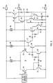
- FIG. 1 is a schematic diagram of a typical low dropout IC voltage regulator.
- the circuit is typically manufactured using a silicon epitaxial planar, PN junction isolated, construction which is well known in the art.
- the circuit receives a + input at terminal 10, referenced against ground terminal 11, and provides a regulated output at terminal 12.
- PNP pass transistor 13 has an area that is from 25 to several hundred times that of a minimum area device.
- the base of transistor 13 is driven by a common emitter NPN driver 14, which has a biasing resistor 15 connected between its base and emitter. This resistor sets the current flowing in transistor 17.
- Emitter resistor 16 degenerates the gain in transistor 14 and this transistors collector current is set by source 38.
- Common collector NPN transistor 17 acts as an emitter follower that drives the base of transistor 14 through resistor 18.
- PNP transistor 19 acts as a bias level shifting emitter follower that drives the base of transistor 17.
- Current source 20 sets the emitter current in transistor 19.
- a differential amplifier (diff-amp) 21 forms the amplifier input stage.
- the currents in transistors 22 and 23, which respectively form the noninverting and inverting inputs, are set by the tail current source 24.
- NPN transistors 25 and 26 form a current mirror load in input stage 21.
- Load input transistor 25 is diode-connected and includes base resistor 27.
- Load output transistor 26 and the output of transistor 23 provide a single ended drive for the base of transistor 19.
- Transistor 26 also includes base resistor 28 and a frequency compensation network composed of resistor 29 and capacitor 30.
- a conventional bandgap reference circuit 31 produces a temperature independent constant voltage which is connected to the base of transistor 22.
- This reference voltage is typically 1.25 volts.
- Resistors 32 and 33 form a voltage divider connected between output termnal 12 and ground.
- the divider tap, node 34 is connected to the base of transistor 23 to provide the regulator negative feedback which stabilizes the circuit operation.
- the output voltage at terminal 12 will be driven to that level, which results in the voltage at node 34 being equal to the reference voltage at the base of transistor 22. Since a high-gain, negative feedback loop is involved, the output voltage will be held constant regardless of changes in temperature, input voltage and regulator load current.
- a PNP transistor such as element 13 goes into saturation, its construction is such that it will inject minority carriers into the IC chip N type epitaxial region. These carriers are collected by the P type isolation material and thereby flow into the chip substrate. This substrate current can cause voltage drops along the chip which can adversely affect adjacent active devices. Furthermore, this excessive substrate current is lost and contributes nothing to the output current. Thus, it only serves to heat the IC chip and represents a reduction in efficiency. Accordingly, a circuit action is incorporated into the structure to reduce or avoid saturation in transistor 13. This circuit action is designated a "saturation catcher" and is accomplished by transistor 35 which operates in the following manner.
- PNP transistor 35 has its emitter connected to the collector of transistor 13 and its base is connected to the base of transistor 13. Under normal operating conditions sat catcher 35 will be off. As transistor 13 approaches saturation, and its collector rises above its base, saturation catcher 35 will turn on and supply current to the base of transistor 36, which will thereby conduct and pull the base of transistor 14 down which will reduce the drive to the base of transistor 13 which rises. When the saturation catcher 35 is off, during normal circuit operation, resistor 37 returns the base of transistor 36 to ground thereby turning it off. It can be seen that conduction in saturation catcher 35 will clamp the collector of transistor 13 at a potential equal to V BE13 -V BE35 . This means that the regulator regulator dropout potential is increased from V SAT of transistor 13 base to emitter potential differential between transistors 13 and 35 which, while higher than V SAT , is still well below V BE .
- Figure 2 is a graph showing the performance of the figure 1 circuit at 25°C.
- Curve 39 is a plot of the V BE of transistor 13.
- Curve 40 shows a theoretical linear plot of 60 mv/decade which serves to show the departure of the V BE of transistor 13 from theoretical impurity, at the higher currents.
- Curve 41 is a plot of the V BE of transistor 35. The regulator dropout voltage would be curve 41 subtracted from curve 39. Clearly, at high currents, the V BE of transistor 13 dominates the dropout voltage.
- a voltage regulator employs a saturation catcher circuit which avoids heavy saturation in the PNP pass transistor.
- a small portion of the pass transistor current is mirrored into the saturation catcher transistor so that its V BE rises along with pass transistor current. Accordingly, the dropout voltage does not rise as steeply with current as is the case where the saturation catcher current .
- Figure 1 is a schematic diagram of a prior art voltage regulator IC that employs a PNP pass transistor and a saturation catcher.
- Figure 2 is a graph showing the V BE of the PNP pass transistor and the saturation catcher of figure 1 as a function of output current.
- Figure 3 is a schematic diagram of the circuit of the invention.
- Figure 4 is a graph showing the V BE of the PNP pass transistor and the saturation catcher of Figure 3 as a function of output current.
- FIG. 5 is a schematic diagram of an alternative circuit employing the invention.
- transistor 42 has its base-emitter circuit in parallel with that of PNP pass transistor 13 and will mirror a small fraction of the regulator V OUT terminal 12 current. Therefore, the current flowing into current mirror 41 will vary with regulator load current. Transistor 42 is made to be a small fraction of the size of transistor 13 (a typical ratio is 1/400) so that a small current proportional to output load current will flow into the current mirror 41. The reflected output current flows in diode connected transistor 43 and resistor 45. Under dropout conditions mirror 41, output transistor 44 and resistor 46 will then sink a variable current from sat catcher 35, which no longer operates at a relatively constant current.
- Figure 5 is a schematic diagram of an alternative circuit using the invention.
- saturation catcher 35' is connected differently. Its base is connected to the base of transistor 13 its collector is returned to the collector of transistor 25 and its emitter is returned via a relatively small value (on the order of 200 ohms) resistor 48 to the collecxtor or transistor 13.
- the collector of transistor 44 is connected to the juncture of the emitter of the catcher 35' and resistor 48.
- catcher 35' will turn on and inject current into the collector of transistor 25. This injected current will offset the error amplifier in such a way as to reduce the base drive to the pass PNP transistor 13.
- the collector current of transistor 44 which tracks the regulator load current, flows in resistor 48, thereby producing a voltage drop which will add to the V BE of of the catcher 35'.
- the V BE of catcher 35' remains relatively constant and the voltage drop across resistor 48 provides the dynamic dropout reduction.
- the circuit of figure 5 was constructed using conventional monolithic silicon IC construction with planar, epitaxial, pn junction isolated parts.
- PNP pass transistor 13 had an area of about 400 times that of transistor 42 so that at an output of 150 ma, the current in transistor 42 was about 0.4 ma.
- COMPONENT VALUE Resistor 16 18 ohms Resistor 18 0 ohms Current Source 20 3 microamperes Current Source 24 6 microamperes Resistor 27 110 ohms Resistor 28 100 ohms Resistor 29 350 ohms Capacitor 30 40 pf Current Source 38 3 microamperes Resistor 32 135.7k ohms Resistor 33 42.9k ohms Resistor 45 1.0k ohms Resistor 46 2.0k ohms Resistor 48 400 ohms In place of resistor 15, an 0.06uA current source was used from the base of transistor 14 to ground. The circuit produced a regulated output of 5 volts and could supply over 150 ma without saturating transistor 13. The maximum dropout voltage at 150 ma was 250 ma millivolts. With transistor 44 disabled, the dropout was 100mv higher.
Landscapes
- Engineering & Computer Science (AREA)
- Microelectronics & Electronic Packaging (AREA)
- Physics & Mathematics (AREA)
- Power Engineering (AREA)
- Nonlinear Science (AREA)
- Electromagnetism (AREA)
- General Physics & Mathematics (AREA)
- Radar, Positioning & Navigation (AREA)
- Automation & Control Theory (AREA)
- Continuous-Control Power Sources That Use Transistors (AREA)
Abstract
Claims (4)
- Circuit intégré incluant un régulateur de tension comprenant un transistor PNP ballast (13) et un transistor PNP d'accrochage de saturation (35) ayant un émetteur raccordé au collecteur du transistor ballast, une base raccordée à la base du transistor ballast, et un collecteur ; caractérisé par un moyen (41) raccordé au transistor d'accrochage de saturation pour faire varier le courant qui s'y écoule en proportion du courant s'écoulant dans le transistor ballast (13), ce par quoi la tension de base-émetteur du transistor d'accrochage de saturation (35) s'élève avec une augmentation du courant de transistor dans le transistor ballast (13).
- Circuit intégré selon la revendication 1, dans lequel ledit moyen (41) comprend : un transistor PNP source de courant (42) dont le trajet émetteur-base est connecté en parallèle avec celui du transistor ballast (13), ce par quoi un courant de détection prend source dans le collecteur du transistor source de courant (42) ; et un miroir de courant NPN (41) dont une entrée est raccordée au collecteur dudit transistor source de courant (42), ce par quoi le miroir de courant NPN (41) dissipe le courant qui prend source dans ledit transistor source (42), et dont une sortie dissipe un courant proportionnel au courant dissipé au niveau de ladite entrée, ladite sortie étant connectée au collecteur du transistor d'accrochage de saturation (35).
- Circuit intégré selon la revendication 2, dans lequel ledit transistor ballast (13) est d'une superficie beaucoup plus grande que ledit transistor source de courant (42), ce par quoi ledit courant de détection est une faible fraction du courant régulateur s'écoulant dans le transistor ballast (13).
- Circuit intégré selon la revendication 2 ou 3, dans lequel une résistance (48) est raccordée en série avec l'émetteur du transistor d'accrochage de saturation (35'), et dans lequel la sortie du miroir de courant NPN (41) est connectée à l'émetteur du transistor d'accrochage de saturation (35').
Applications Claiming Priority (3)
| Application Number | Priority Date | Filing Date | Title |
|---|---|---|---|
| US36777 | 1993-03-25 | ||
| US08/036,777 US5410241A (en) | 1993-03-25 | 1993-03-25 | Circuit to reduce dropout voltage in a low dropout voltage regulator using a dynamically controlled sat catcher |
| PCT/US1994/003250 WO1994022068A1 (fr) | 1993-03-25 | 1994-03-24 | Circuit d'abaissement de la tension de relachement dans un regulateur a faible tension de relachement |
Publications (2)
| Publication Number | Publication Date |
|---|---|
| EP0691004A1 EP0691004A1 (fr) | 1996-01-10 |
| EP0691004B1 true EP0691004B1 (fr) | 1997-05-28 |
Family
ID=21890598
Family Applications (1)
| Application Number | Title | Priority Date | Filing Date |
|---|---|---|---|
| EP94912304A Expired - Lifetime EP0691004B1 (fr) | 1993-03-25 | 1994-03-24 | Circuit d'abaissement de la tension de relachement dans un regulateur a faible tension de relachement |
Country Status (4)
| Country | Link |
|---|---|
| US (1) | US5410241A (fr) |
| EP (1) | EP0691004B1 (fr) |
| DE (1) | DE69403465T2 (fr) |
| WO (1) | WO1994022068A1 (fr) |
Families Citing this family (24)
| Publication number | Priority date | Publication date | Assignee | Title |
|---|---|---|---|---|
| JPH07114423A (ja) * | 1993-10-14 | 1995-05-02 | Fujitsu Ltd | 基準電源回路 |
| DE69326698T2 (de) * | 1993-12-17 | 2000-02-10 | St Microelectronics Srl | Bandlückenspannungsreferenz mit niedriger Versorgungsspannung |
| US5552740A (en) * | 1994-02-08 | 1996-09-03 | Micron Technology, Inc. | N-channel voltage regulator |
| US5506496A (en) * | 1994-10-20 | 1996-04-09 | Siliconix Incorporated | Output control circuit for a voltage regulator |
| US5672962A (en) * | 1994-12-05 | 1997-09-30 | Texas Instruments Incorporated | Frequency compensated current output circuit with increased gain |
| DE19535807C1 (de) * | 1995-09-26 | 1996-10-24 | Siemens Ag | Schaltungsanordnung zur Erzeugung eines Biaspotentials |
| US5781002A (en) * | 1996-02-23 | 1998-07-14 | Linear Technology Corporation | Anti-latch circuit for low dropout dual supply voltage regulator |
| US5808458A (en) * | 1996-10-04 | 1998-09-15 | Rohm Co., Ltd. | Regulated power supply circuit |
| US5804958A (en) * | 1997-06-13 | 1998-09-08 | Motorola, Inc. | Self-referenced control circuit |
| US6271711B1 (en) * | 1999-09-01 | 2001-08-07 | Lsi Logic Corporation | Supply independent biasing scheme |
| US6218822B1 (en) | 1999-10-13 | 2001-04-17 | National Semiconductor Corporation | CMOS voltage reference with post-assembly curvature trim |
| US6329804B1 (en) | 1999-10-13 | 2001-12-11 | National Semiconductor Corporation | Slope and level trim DAC for voltage reference |
| US6201379B1 (en) | 1999-10-13 | 2001-03-13 | National Semiconductor Corporation | CMOS voltage reference with a nulling amplifier |
| US6198266B1 (en) | 1999-10-13 | 2001-03-06 | National Semiconductor Corporation | Low dropout voltage reference |
| US6522111B2 (en) | 2001-01-26 | 2003-02-18 | Linfinity Microelectronics | Linear voltage regulator using adaptive biasing |
| US7030598B1 (en) * | 2003-08-06 | 2006-04-18 | National Semiconductor Corporation | Low dropout voltage regulator |
| US6894472B2 (en) | 2003-08-20 | 2005-05-17 | Broadcom Corporation | Low leakage CMOS power mux |
| US6879142B2 (en) * | 2003-08-20 | 2005-04-12 | Broadcom Corporation | Power management unit for use in portable applications |
| US7161339B2 (en) * | 2003-08-20 | 2007-01-09 | Broadcom Corporation | High voltage power management unit architecture in CMOS process |
| US7285940B2 (en) * | 2005-09-07 | 2007-10-23 | Nxp B.V. | Voltage regulator with shunt feedback |
| CN103616916A (zh) * | 2013-11-27 | 2014-03-05 | 苏州贝克微电子有限公司 | 一种低电压差稳压器的电压差的电路 |
| US9645594B2 (en) * | 2015-10-13 | 2017-05-09 | STMicroelectronics Design & Application S.R.O. | Voltage regulator with dropout detector and bias current limiter and associated methods |
| US10203708B2 (en) * | 2015-11-30 | 2019-02-12 | Rohm Co., Ltd. | Power regulator to control output voltage using feedback |
| EP4009132A1 (fr) * | 2020-12-03 | 2022-06-08 | NXP USA, Inc. | Circuit de tension de référence de barrière de potentiel |
Family Cites Families (9)
| Publication number | Priority date | Publication date | Assignee | Title |
|---|---|---|---|---|
| US4345166A (en) * | 1979-09-28 | 1982-08-17 | Motorola, Inc. | Current source having saturation protection |
| US4532467A (en) * | 1983-03-14 | 1985-07-30 | Vitafin N.V. | CMOS Circuits with parameter adapted voltage regulator |
| JPS6091425A (ja) * | 1983-10-25 | 1985-05-22 | Sharp Corp | 定電圧電源回路 |
| US4626770A (en) * | 1985-07-31 | 1986-12-02 | Motorola, Inc. | NPN band gap voltage reference |
| US4794277A (en) * | 1986-01-13 | 1988-12-27 | Unitrode Corporation | Integrated circuit under-voltage lockout |
| JP2595545B2 (ja) * | 1987-07-16 | 1997-04-02 | ソニー株式会社 | 定電圧回路 |
| US5248932A (en) * | 1990-01-13 | 1993-09-28 | Harris Corporation | Current mirror circuit with cascoded bipolar transistors |
| US5084668A (en) * | 1990-06-08 | 1992-01-28 | Motorola, Inc. | System for sensing and/or controlling the level of current in a transistor |
| FR2672705B1 (fr) * | 1991-02-07 | 1993-06-04 | Valeo Equip Electr Moteur | Circuit generateur d'une tension de reference variable en fonction de la temperature, notamment pour regulateur de la tension de charge d'une batterie par un alternateur. |
-
1993
- 1993-03-25 US US08/036,777 patent/US5410241A/en not_active Expired - Lifetime
-
1994
- 1994-03-24 EP EP94912304A patent/EP0691004B1/fr not_active Expired - Lifetime
- 1994-03-24 DE DE69403465T patent/DE69403465T2/de not_active Expired - Lifetime
- 1994-03-24 WO PCT/US1994/003250 patent/WO1994022068A1/fr active IP Right Grant
Also Published As
| Publication number | Publication date |
|---|---|
| EP0691004A1 (fr) | 1996-01-10 |
| US5410241A (en) | 1995-04-25 |
| DE69403465D1 (de) | 1997-07-03 |
| WO1994022068A1 (fr) | 1994-09-29 |
| DE69403465T2 (de) | 1998-01-22 |
Similar Documents
| Publication | Publication Date | Title |
|---|---|---|
| EP0691004B1 (fr) | Circuit d'abaissement de la tension de relachement dans un regulateur a faible tension de relachement | |
| JP2863566B2 (ja) | 電圧調整回路 | |
| US5548205A (en) | Method and circuit for control of saturation current in voltage regulators | |
| US4008441A (en) | Current amplifier | |
| US4528496A (en) | Current supply for use in low voltage IC devices | |
| US3648154A (en) | Power supply start circuit and amplifier circuit | |
| US4327319A (en) | Active power supply ripple filter | |
| US3500220A (en) | Sense amplifier adapted for monolithic fabrication | |
| US6680643B2 (en) | Bandgap type reference voltage source with low supply voltage | |
| US4567444A (en) | Current mirror circuit with control means for establishing an input-output current ratio | |
| JPH0618015B2 (ja) | 電 流 安 定 化 回 路 | |
| US4390829A (en) | Shunt voltage regulator circuit | |
| US5023543A (en) | Temperature compensated voltage regulator and reference circuit | |
| US3947704A (en) | Low resistance microcurrent regulated current source | |
| EP0306134B1 (fr) | Générateur courant de précision-commandé | |
| US6144250A (en) | Error amplifier reference circuit | |
| US4433283A (en) | Band gap regulator circuit | |
| US4786827A (en) | Antisaturation circuit for integrated PNP transistor with intervention characteristic definable according to a preset function | |
| US3031608A (en) | Voltage regulator | |
| US5920184A (en) | Low ripple voltage reference circuit | |
| US4103220A (en) | Low dissipation voltage regulator | |
| US4172992A (en) | Constant current control circuit | |
| US4570114A (en) | Integrated voltage regulator | |
| US4553107A (en) | Current mirror circuit having stabilized output current | |
| US4112346A (en) | Constant current circuit |
Legal Events
| Date | Code | Title | Description |
|---|---|---|---|
| PUAI | Public reference made under article 153(3) epc to a published international application that has entered the european phase |
Free format text: ORIGINAL CODE: 0009012 |
|
| 17P | Request for examination filed |
Effective date: 19950801 |
|
| AK | Designated contracting states |
Kind code of ref document: A1 Designated state(s): DE FR GB |
|
| GRAG | Despatch of communication of intention to grant |
Free format text: ORIGINAL CODE: EPIDOS AGRA |
|
| 17Q | First examination report despatched |
Effective date: 19960628 |
|
| GRAH | Despatch of communication of intention to grant a patent |
Free format text: ORIGINAL CODE: EPIDOS IGRA |
|
| GRAH | Despatch of communication of intention to grant a patent |
Free format text: ORIGINAL CODE: EPIDOS IGRA |
|
| GRAA | (expected) grant |
Free format text: ORIGINAL CODE: 0009210 |
|
| AK | Designated contracting states |
Kind code of ref document: B1 Designated state(s): DE FR GB |
|
| PG25 | Lapsed in a contracting state [announced via postgrant information from national office to epo] |
Ref country code: FR Effective date: 19970528 |
|
| REF | Corresponds to: |
Ref document number: 69403465 Country of ref document: DE Date of ref document: 19970703 |
|
| EN | Fr: translation not filed | ||
| PG25 | Lapsed in a contracting state [announced via postgrant information from national office to epo] |
Ref country code: GB Free format text: LAPSE BECAUSE OF NON-PAYMENT OF DUE FEES Effective date: 19980324 |
|
| PLBE | No opposition filed within time limit |
Free format text: ORIGINAL CODE: 0009261 |
|
| STAA | Information on the status of an ep patent application or granted ep patent |
Free format text: STATUS: NO OPPOSITION FILED WITHIN TIME LIMIT |
|
| 26N | No opposition filed | ||
| GBPC | Gb: european patent ceased through non-payment of renewal fee |
Effective date: 19980324 |
|
| PGFP | Annual fee paid to national office [announced via postgrant information from national office to epo] |
Ref country code: DE Payment date: 20120328 Year of fee payment: 19 |
|
| REG | Reference to a national code |
Ref country code: DE Ref legal event code: R082 Ref document number: 69403465 Country of ref document: DE |
|
| REG | Reference to a national code |
Ref country code: DE Ref legal event code: R119 Ref document number: 69403465 Country of ref document: DE Effective date: 20131001 |
|
| PG25 | Lapsed in a contracting state [announced via postgrant information from national office to epo] |
Ref country code: DE Free format text: LAPSE BECAUSE OF NON-PAYMENT OF DUE FEES Effective date: 20131001 |