EP0690554B1 - Redundanter Leistungsmischer mit Fehlererkennung für Gleichstromwandler - Google Patents
Redundanter Leistungsmischer mit Fehlererkennung für Gleichstromwandler Download PDFInfo
- Publication number
- EP0690554B1 EP0690554B1 EP95304573A EP95304573A EP0690554B1 EP 0690554 B1 EP0690554 B1 EP 0690554B1 EP 95304573 A EP95304573 A EP 95304573A EP 95304573 A EP95304573 A EP 95304573A EP 0690554 B1 EP0690554 B1 EP 0690554B1
- Authority
- EP
- European Patent Office
- Prior art keywords
- power
- current
- enabling
- circuit
- coupled
- Prior art date
- Legal status (The legal status is an assumption and is not a legal conclusion. Google has not performed a legal analysis and makes no representation as to the accuracy of the status listed.)
- Expired - Lifetime
Links
- 238000001514 detection method Methods 0.000 title 1
- 230000004044 response Effects 0.000 claims description 15
- 230000005669 field effect Effects 0.000 claims description 3
- 229910044991 metal oxide Inorganic materials 0.000 claims description 3
- 150000004706 metal oxides Chemical class 0.000 claims description 3
- XUIMIQQOPSSXEZ-UHFFFAOYSA-N Silicon Chemical compound [Si] XUIMIQQOPSSXEZ-UHFFFAOYSA-N 0.000 claims description 2
- 229910052710 silicon Inorganic materials 0.000 claims description 2
- 239000010703 silicon Substances 0.000 claims description 2
- 238000002955 isolation Methods 0.000 description 9
- 238000012360 testing method Methods 0.000 description 8
- 238000010586 diagram Methods 0.000 description 5
- 230000008878 coupling Effects 0.000 description 3
- 238000010168 coupling process Methods 0.000 description 3
- 238000005859 coupling reaction Methods 0.000 description 3
- 230000007274 generation of a signal involved in cell-cell signaling Effects 0.000 description 3
- 238000012423 maintenance Methods 0.000 description 3
- 239000003990 capacitor Substances 0.000 description 2
- 230000008859 change Effects 0.000 description 2
- 230000002950 deficient Effects 0.000 description 2
- 238000012986 modification Methods 0.000 description 2
- 230000004048 modification Effects 0.000 description 2
- 230000009977 dual effect Effects 0.000 description 1
- 238000003780 insertion Methods 0.000 description 1
- 230000037431 insertion Effects 0.000 description 1
- 230000007257 malfunction Effects 0.000 description 1
- 238000000034 method Methods 0.000 description 1
- 230000008569 process Effects 0.000 description 1
- 239000004065 semiconductor Substances 0.000 description 1
Images


Classifications
-
- H—ELECTRICITY
- H02—GENERATION; CONVERSION OR DISTRIBUTION OF ELECTRIC POWER
- H02H—EMERGENCY PROTECTIVE CIRCUIT ARRANGEMENTS
- H02H9/00—Emergency protective circuit arrangements for limiting excess current or voltage without disconnection
- H02H9/001—Emergency protective circuit arrangements for limiting excess current or voltage without disconnection limiting speed of change of electric quantities, e.g. soft switching on or off
- H02H9/004—Emergency protective circuit arrangements for limiting excess current or voltage without disconnection limiting speed of change of electric quantities, e.g. soft switching on or off in connection with live-insertion of plug-in units
-
- H—ELECTRICITY
- H02—GENERATION; CONVERSION OR DISTRIBUTION OF ELECTRIC POWER
- H02J—CIRCUIT ARRANGEMENTS OR SYSTEMS FOR SUPPLYING OR DISTRIBUTING ELECTRIC POWER; SYSTEMS FOR STORING ELECTRIC ENERGY
- H02J1/00—Circuit arrangements for DC mains or DC distribution networks
- H02J1/001—Hot plugging or unplugging of load or power modules to or from power distribution networks
-
- H—ELECTRICITY
- H02—GENERATION; CONVERSION OR DISTRIBUTION OF ELECTRIC POWER
- H02J—CIRCUIT ARRANGEMENTS OR SYSTEMS FOR SUPPLYING OR DISTRIBUTING ELECTRIC POWER; SYSTEMS FOR STORING ELECTRIC ENERGY
- H02J1/00—Circuit arrangements for DC mains or DC distribution networks
- H02J1/10—Parallel operation of DC sources
-
- H—ELECTRICITY
- H02—GENERATION; CONVERSION OR DISTRIBUTION OF ELECTRIC POWER
- H02H—EMERGENCY PROTECTIVE CIRCUIT ARRANGEMENTS
- H02H3/00—Emergency protective circuit arrangements for automatic disconnection directly responsive to an undesired change from normal electric working condition with or without subsequent reconnection ; integrated protection
- H02H3/02—Details
- H02H3/05—Details with means for increasing reliability, e.g. redundancy arrangements
Definitions
- the present invention relates generally to mixing of power supplied by multiple power supplies.
- Fault tolerant computer systems are commonly designed such that component failures occurring in 1 area of the system are prevented from affecting the remaining areas of the system. Further, fault tolerant computer systems are typically designed to continue operations and maintain data integrity even when a faulty component is being serviced.
- UPSs uninterruptable power supplies
- CRUs customer replaceable units
- LU logic units
- US-A-4614877 discloses a power mixing apparatus coupled to a backplane for mixing current from a first power rail and current from a second power rail, the power mixing apparatus including first and second pairs of pins.
- the present invention seeks to provide a power mixing apparatus enabling switching of power source input from alternative power supplies and protecting other portions of the LU circuitry from power transients and other power fluctuations, such as 'hot' removal of the LU.
- a power mixing apparatus coupled to a backplane for mixing current from a first power rail and current from a second power rail
- the power mixing apparatus including first and second pairs of pins characterised by:
- a power mixing apparatus includes a first and second enabling circuit for producing a first and a second enabling signal to select whether power is supplied from a first and/or second power supply, respectively; a first and second inrush limiter for limiting the time rate of change of current flowing from the first and second power supplies to a direct-current converter, in response to the first and second enabling signals, respectively; a first open-circuiting circuit for coupling the first inrush limiter and the direct-current converter to the first enabling circuit, when the first open circuiting circuit is coupled to a first pair of shorting pins; a second open-circuiting circuit for coupling the second inrush limiter and the direct-current converter to the second enabling circuit, when the second open-circuiting circuit is coupled to a second pair of shorting pins; wherein the first and second pair of shorting pins are coupled to the first and second open-circuiting circuits, respectively, only when the LU is fully inserted into a computer housing.
- the first and second inrush limiters include metal oxide silicon field effect transistors
- the first and second open-circuiting circuit are opto-isolators
- the first and second pair of shorting pins are a short-circuit connection.
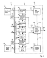
- Fig. 1 illustrates a Logic Unit (LU) 10 as including a power mixing circuit 14.
- the LU 10 is a larger unit containing or carrying other functional equipment that is powered by the power mixing circuit 14 such as for example a secondary storage unit (disk).
- the LU 10 is structured to be removable inserted in a cabinet or like structure that has a receiving connection typically in the form of a backplane 5.
- Backplane 5 includes first and second power rails 15 and 25, first and second signal lines 35 and 45, and a connector (not shown) that includes first and second pairs of short pins 73 and 83.
- a first power supply 20 is coupled to first power rail 15, and a second power supply 30 is coupled to second power rail 25.
- First power rail 15, second power rail 25, first signal line 35, and second signal line 45 are electrically decoupled from power mixing circuit 14, when LU 10 is physically decoupled from backplane 5.
- Power mixing circuit 14 includes a first and a second enabling circuit 40 and 50 respectively coupled to receive signal lines 35 and 45 via signal lines 23 and 33.
- the first and second enabling circuits 40 and 50 are coupled to a maintenance logic unit (MLU) 130 via signal lines 21 and 31, respectively.
- MLU maintenance logic unit
- First enabling circuit 40 operates to assert a first enabling signal
- second enabling circuit 50 operates to assert a second enabling signal in response to an enabling signal on signal lines 23 or 33, or signal lines 21 or 31, respectively.
- a first inrush limiter 60 is coupled to the first power rail 15 by backplane 5, and a second inrush limiter 70 is similarly coupled to the power rail 25 - also by the backplane 5.
- First inrush limiter 60 when enabled, operates to limit the time rate of change of current flowing from first power rail 15, also known as current slew rate. Enabling the second inrush limiter 70 will limit the current slew rate flowing from second power rail 25.
- first inrush limiter 60 and second inrush limiter 70 also limit the maximum amount of current flowing from first power rail 15 and second power rail 25, respectively.
- a first open-circuiting circuit 80 is coupled to first enabling circuit 40 by signal line 75, to first inrush limiter 60 by signal line 77, and to backplane 5 by the first pair of short pins 73.
- First open-circuiting circuit 80 is adapted to electrically couple first enabling circuit 40 to first inrush limiter 60 so long as first open-circuiting circuit 80 is coupled to first pair of short pins 73.
- a second open-circuiting circuit 90 is coupled to second enabling circuit 50 by signal line 85, to second inrush limiter 70 by signal line 87, and to backplane 5 by a second pair of short pins 83.
- Second open-circuiting circuit 90 is adapted to electrically couple second enabling circuit 50 to second inrush limiter 80 so long as second open-circuiting circuit 90 is coupled to second pair of short pins 83.
- Power mixing circuit 14 also includes a first isolation circuit 100 coupled to first inrush limiter 60 by power line 95, and a second isolation circuit 110 coupled to second inrush limiter 70 by power line 105.
- First isolation circuit 100 is adapted to isolate first inrush limiter 60 and other circuitry associated with first power supply 20 from power associated with second power supply 30.
- Second isolation circuit 110 is adapted to isolate second inrush limiter 70 and other circuitry associated with second power supply 30 from power associated with first power supply 20.
- a direct-current converter (DCC) 120 is coupled to first open-circuiting circuit 80 by signal line 113, to second open-circuiting circuit 90 by signal line 115, to first isolation circuit 100 by power line 117, and to second isolation circuit 110 by power line 119.
- DCC 120 is adapted to convert direct current power from power line 117 or from power line 119 into a direct current output 160, when DCC 120 is enabled.
- the first pair and second of short pins 73 and 83 are coupled to the first and the second open circuiting circuits 80 and 90, respectively.
- the corresponding first and second open-circuiting circuits 80 and 90 will respectively couple the outputs of the first and the second enabling circuit 40 and 50 to an enable input of the first and the second inrush limiters 60 and 70 via signal lines 77 and 87.
- the outputs of the first and the second enabling circuits 40 and 50 to the enable input of the DCC 120 via signal lines 113 and 115.
- asserting enabling signals on signal lines 35 or 45 will cause the enabling circuits 40,50 to enable the first and or second inrush limiters 60 and 70 and DCC 120.
- a LU 10 is initially installed into the computer (not shown) coupling it to backplane 5.
- First power supply 20 supplies power to first power rail 15 and second power supply 30 supplies power to second power rail 25.
- the computer asserts an enabling signal on signal line 35 enabling LU 10 to draw power from first power rail 15, and the computer asserts an enabling signal on signal line 45 enabling LU 10 to draw power from second power rail 25. More specifically the enabling signal carried by signal line 35 enables first enabling circuit 40 to generate a first enabling signal, and in similar fashion the enabling signal carried by signal line 45 enables second enabling circuit 50 to generate a second enabling signal.
- first inrush limiter 60 When first inrush limiter 60 is enabled, the current slew rate from power rail 15 to power line 95 is limited. Similarly, enabling second inrush limiter 70 will limit the current slew rate from power rail 25 to power line 105 also. If first inrush limiter 60 or second inrush limiter 70 are not enabled, power draw from power rail 25 and power rail 35 are respectively inhibited.
- first isolation circuit 100 When power flows on power line 95, first isolation circuit 100 allows power to flow on power line 117 to DCC 120. When power flows on power line 105, second isolation circuit 110 allows power to flow on power line 119 to DCC 120.
- DCC 120 When DCC 120 is enabled, either by the first enabling signal or the second enabling signal, DCC 120 converts power from power rail 117 or power rail 119, without distinguishing where the power is derived from, to a DCC output 160.
- the LU 10, so structured, is capable of being removed from the power supplies 20 and 30 in a manner that prevents power surges, arcing and like occurrences that can damage the LU 10, the computer (not shown) to which it attaches, or other associated circuitry, in the following manner.
- LU 10 In the normal operating mode, LU 10 is fully coupled to backplane 5. If a user begins to remove LU 10 from backplane 5, initially a first pair of shorting pins 73 are electrically decoupled from first open-circuiting circuit 80 and second pair of shorting pins 83 are electrically decoupled from second open-circuiting circuit 90, meanwhile first inrush limiter 60 remains coupled to first power rail 15 and second inrush limiter 70 remains coupled to second power rail 25.
- first open-circuiting circuit 80 decouples first enabling circuit 40 from first inrush limiter 60 and DCC 120
- second open-circuiting circuit 90 decouples second enabling circuit 50 from second inrush limiter 70 and DCC 120.
- DCC 120 does not draw power from first power rail 15 or second power rail 25, and the LU 10 is effectively turned off. The user can then safely continue to remove LU 10 from the computer system, thereby decoupling the LU 10 from power rail 15 and power rail 25 and the rest of backplane 5.
- Power rail 15 is coupled to first inrush limiter 60 and power rail 25 is coupled to second inrush limiter 70, before first pair of shorting pins 73 are coupled to first open-circuiting circuit 80 or second pair of shorting pins 83 are coupled to second open-circuiting circuit 90. Since the respective power rails are coupled to LU 10, before LU 10 begins to draw power, arcing of the power rails to LU 10 is reduced.
- the function of first pair of shorting pins 73 and second pair of shorting pins 83 are known as "break-first, make-last" connections.
- Fig. 2 is a schematic diagram of one embodiment of the invention.
- power mixing circuit 14 receives control signals SPI-SEL0 and SPI-SEL1 on signal lines 35 and 45, respectively. Additional control inputs for receiving other control signals in addition to the SPI-SEL signals are not shown.
- the control signals are standard logic-level signals.
- the first and second power supplies are typically direct-current sources and can be derived from a battery or from the general power supply.
- a positive voltage convention is used to avoid confusion; however it will be evident to those skilled in this art that the voltage on power rails 15 and 25 may be negative, such as -48 volts. (In fact, Fig. 3, as will be seen, uses a negative voltage convention.)
- First pair of short pins 73 are a pair of pins 74 and 75 that are electrically shorted together.
- Second pair of short pins 83 are a pair of pins 84 and 85 that are electrically shorted together.
- the physical length of pins 74, 75, 84, and 85 are shorter than the length of the other pins on backplane 5. If LU 10 is partially removed from backplane 5, pins 74, 75, 84, and 85 will loose physical and electrically connection with LU 10 before the remaining pins of backplane 5, such as first power rail 15 or second power rail 25, loose connection with LU 10.
- the first enabling signal and second enabling signal are electrically decoupled from other portions of power mixing circuit 14.
- the SPI-SEL0 signal on signal line 35 is coupled to a control input of the first and second enabling circuits 40, 50 and and to a first logic input of the maintenance logic unit (MLU) 130 by signal line 23.
- the SPI-SEL1 signal on signal line 45 is also coupled to a control input of first and second enabling circuits 40,50 and to a second logic input of maintenance logic unit (MLU) 130 by a by signal line 33.
- the first and second enabling circuits 40,50 are embodied as opto-isolators 41 and 51, respectively.
- MLU 130 has first and second power control outputs with the first control output coupled to the control input of the first opto-isolator 41 by a first MLU signal line 21 and the second control output is coupled to the control input of the second opto-isolator 51 by a second MLU signal line 31.
- Inputs to opto-isolator 41 and 51 are arranged in a wired "OR" arrangement to receive inputs from SPI-SEL0, SPI-SEL1, and MLU 130.
- Signal lines 23, 33 and 21 serve to enable the first enabling circuit
- signal lines 23, 33, and 31 serve to enable the second enabling circuit.
- the first power rail 15 enters the LU 10 through a first current limiter 60, embodied as a power pass transistor, and is coupled to the power input of a DC controller (DCC) 120 via a first protection diode 102 and a first fuse 104, coupled in series.
- a second power rail 25 enters the LU 10 through a second current limiter 70, embodied as a power pass transistor, and is coupled to the input of the DCC 120 via a second protection diode 112 and a second fuse 114, coupled in series.
- a DCC 120 enable input is coupled to a collector lead of the first opto-isolator 41 and the gate of the first power pass transistor 60 via a first control diode 161.
- DCC 120 enable input is also coupled to a collector lead of the second opto-isolator 51, and the gate of the second power pass transistor 70 via a second control diode 163.
- the enable input DCC 120 is also connected to a Vcc terminal 140 via pull-up resistor 150.
- First control diode 161 prevents the first enabling signal from enabling second current limiter 70, and second control diode 163 prevents the second enabling signal from enabling first current limiter 60.
- a rail OK signal generation circuit 170 includes a first test opto-isolator 180 having a control input coupled to a first test node 183 located between the output of first power pass transistor 60 and the input of first protection diode 102 and having an output coupled to a first test input of MLU 130 by a first test signal line 185.
- a second test opto-isolator 190 has a control input coupled a second test node 193 located between the output of second power pass transistor 70 and the input of second protection diode 112 and has an output coupled to a second test input of MLU 130 by a second test signal line 195.
- Rail OK signal generation circuit 170 is not shown in Fig. 1.
- a system controller may assert one, or the other, or both of the SPI-SEL signals.
- the SPI-SEL signals When the SPI-SEL signals are asserted (or either of them), the LU 10 then is enabled to respond to other control signals (not shown, and not relevant here).
- both power rails 15 and 25 of the LU 10 can be coupled to the DCC 120 by asserting either SPI-SEL signal because the signals are coupled to both control opto-isolators 41 and 51 by first or second signal lines 23 or 33, respectively.
- the SPI-SEL signals must each have sufficient high-level drive current to be able to power both control opto-isolators 41 and 51.
- the system controller utilizes other control signals (not shown) causing the MLU 130 to assert power control signals on MLU control lines 21 and 31 to opto-isolators 41 and 51 and allowing the negation of the SPI-SEL signals. Accordingly, the SPI-SEL signals perform the dual functions of unit selection and power control.
- control signal on the first MLU control line to the opto-isolator 41 when the control signal on the first MLU control line to the opto-isolator 41 is negated, for example, the first opto-isolator 41 will cease conducting, and the gate of the first power-pass transistor 60 will be pulled to about Vcc. As a result, the first power pass transistor 60 will cease conduction and power will not be drawn from first power rail 15. However, if the second optoisolator 51 continues to conduct, the gate voltage of second power pass transistor 70 is held low, allowing power to be drawn from second power rail 25. Control diode 161 ensures conduction of second opto-isolator 51 does not pull the gate voltage of first power pass transistor 60 low. (Control diode 163 performs the same function to prevent turning on the second power pass transistor 70 by conduction of opto-isolator 41.)
- protection diodes 102 and 112 Since power line 117 and power line 119 are coupled before DCC 120, so long as power line 117 and power line 119 are equally powered, protection diodes 102 and 112 are not needed. However in the case where power is not being drawn from one of the power rails, power rail 15 for example, protection diode 102 ensures, that power from power line 119 does not create a reverse power flow. Conversely, protection diode 112 ensures that power from power line 117 does not create a reverse power flow.
- Protection fuses 104 and 114 ensures that a limited amount of current is drawn from power rails 15 and 20, in the case of a spurious short circuit or other malfunction in DCC 120.
- protection fuses 104 and 114 can be located between power rail 15 and first inrush limiter 60 and between 25 and second inrush limiter 70, respectively, in order to protect the circuitry of power mixing circuit 14.
- the rail OK signal generation circuit 170 permits MLU 130 to monitor the status of power being drawn from first power rail 15 and second power rail 25.
- pins 74 and 75, (and 85, 84) being shorter than the rest e.g., those that communicate the power rails 15 and 25 to the LU 10
- pins 84 and 85 will break the electrical connection between second enabling circuit 50 and power-pass transistor 70, before power-pass transistor 70 breaks electrical connection to power rail 25. Breaking these electrical connections removes enabling signals from DCC 120.
- the LU 10 is already powered down, causing fewer power related problems.
- FIG. 3 is a schematic diagram of another embodiment of the present invention.
- a Logic Unit (LU) 10 including a power mixing circuit 14 is coupled to a backplane 5.
- Backplane 5 includes a first power rail 15, a second power rail 25, a first signal line 35, a power return rail 55, a second signal line 45, and a connector (not shown) that includes a first shorting pin 73, and a second shorting pins 83.
- first power rail 15 and second power rail 25 provide a negative voltage, preferably from -40 to -60 volts.
- First shorting pin 73 and second shorting pin 83 are coupled to power return rail 55 on backplane 5 in a "make-last, break-first" arrangement. Accordingly, first and second shorting pins 73 and 83 operate to couple first and second enabling circuits 40 and 50 to power return rail 55 only after LU 10 is coupled to first and second power rails 15 and 25. Conversely, the first and second shorting pins 73 and 83 will operate to decouple first and second enabling circuits 40 and 50 from power return rail 55 before LU 10 is decoupled from first and second power rails 15 and 25.
- the SPI_SEL0 and SPI_SEL1 signals carried by the signal lines 35 and 45 are provided as in the embodiment in Fig. 2.
- the MLU is not shown in this embodiment.
- a first system enabling signal is asserted when a signal appears on signal line 23 from SPI_SEL0, and a second system enabling signal is asserted when a signal appears on signal line 33 from SPI_SEL1.
- First and second enabling circuits 40 and 50 are adapted to generate a first and second enabling signal, when first and second enabling circuits 40 and 50 are coupled to power return rail 55, and when the first system enabling signal or the second system enabling signal are respectively asserted.
- first and second enabling circuits 40 and 50 are opto-isolators 41 and 51.
- First and second inrush limiters 60 and 70 include fuses 104 and 114, metal oxide semiconductor field effect transistors (MOSFETs) 62 and 72, and gate voltage limiting circuits 64 and 74, respectively.
- Fuses 104 and 114 are adapted to limit the peak current flowing from first and second power rails 15 and 25, respectively.
- MOSFETs 62 and 72 are adapted to allow a first and a second current to be drawn from power rails 15 and 25, in response to a respective gate voltage on MOSFETs 62 and 72.
- First and second gate voltage limiting circuits 64 and 72 are adapted to provide an exponentially increasing gate voltage to MOSFETs 62 and 72 in response to the first and the second enabling signals, respectively.
- First gate voltage limiting circuit 64 includes a resistor 65 and a capacitor 66 which together define the exponential rise-time of the gate voltage when LU 10 is initially installed into the computer. First gate voltage limiting circuit 64 also includes resistor 67 and diode 68 which affect the fall-time of the gate voltage when LU 10 is removed from the computer. Second gate voltage limiting circuit 64 operates in the same manner as first gate voltage limiting circuit 64, with resistors 75 and 77, capacitors 76, and diode 78.
- First and second isolation circuits 100 and 110 are coupled to the first and second current limiters 60 and 70, and operate to electrically isolate the two power rails 15, 25 in the same manner as do diodes 102 and 112, respectively, of Fig. 2.
- DCC 120 is coupled to first and second diodes 102 and 112 and to the power return rail 55, and DCC 120 adapted to convert current from power rail 117 to a direct current output 160 and adapted to convert current from power rail 119 to a direct current output 160.
- Rail OK circuit 170 is similar to the embodiment of the rail OK circuit 170 in Fig. 2.
- first and second enabling circuits 40 and 50 cannot generate the first or second enabling signals, until after LU 10 is fully coupled to first and second power rails 15 and 25.
- first and second enabling circuits 40 and 50 are coupled to power return rail 55. Then in response to a first and/or second system enabling signal, first and/or second enabling circuits 40 and 60 generate a first and/or a second enabling signal, respectively. In response to the first and/or second enabling signals, the gate voltage of MOSFETS 62 and 72 rise exponentially, thus MOSFETS 62 and 72 conduct current exponentially. First and/or second current limiters thus generate a first and/or a second current.
- the first and/or second current pass through diodes 102 and /or 112 and are input into DCC 120, where a direct-current output is produced.
- first and second shorting pins 73 and 74 decouple first and second enabling circuits 40 and 50 from power return rail 55, respectively, therefore, first and second enabling signals are deasserted. Once the enabling signals are deasserted, the gate voltages of MOSFETs 62 and 72 fall rapidly, thus MOSFETs 62 and 72 inhibit current flow. First and second current limiters 60 and 70 thus inhibit current from being drawn from power rails 15 and 25, respectively. Once current draw from power rail 15 and 25 is removed, LU 10 can safely be removed from the computer system.
Landscapes
- Engineering & Computer Science (AREA)
- Power Engineering (AREA)
- Power Sources (AREA)
- Dc-Dc Converters (AREA)
- Direct Current Feeding And Distribution (AREA)
- Control Of Voltage And Current In General (AREA)
- Power Conversion In General (AREA)
Claims (7)
- Energiemischschaltung (14), die mit einer Rückseitenplatine (5) verbunden ist, zum Mischen von Strom aus einer ersten Energieschiene (20) und von Strom aus einer zweiten Energieschiene (30), wobei die Energiemischvorrichtung erste und zweite Stiftepaare (73, 83) enthält, gekennzeichnet durch:wobei die erste Freigabeschaltung mit dem ersten Stiftepaar verbunden ist und dazu dient, die erste Freigabeschaltung elektrisch mit der ersten Strombegrenzungseinrichtung zu verbinden und die erste Freigabeschaltung von der ersten Strombegrenzungseinrichtung zu trennen, wenn das erste Stiftepaar offen ist;eine erste Freigabeschaltung (40), angepasst für die Bereitstellung eines ersten Freigabesignals;eine zweite Freigabeschaltung (50), angepasst für die Bereitstellung eines zweiten Freigabesignals;einen ersten Strombegrenzer (60), der mit der ersten Energieschiene verbunden und dafür angepasst ist, einen ersten Strom aus der ersten Energieschiene als Antwort auf das erste Freigabesignal zu liefern und den ersten Strom zu begrenzen;einen zweiten Strombegrenzer (70), der mit der zweiten Energieschiene verbunden ist, und dafür angepasst ist, einen zweiten Strom aus dem zweiten Gleichstrom als Antwort auf das zweite Freigabesignal zu liefern und den zweiten Strom zu begrenzen;
wobei die zweite Freigabeschaltung mit dem zweiten Stiftepaar verbunden ist und dazu dient, die zweite Freigabeschaltung elektrisch mit der zweiten Strombegrenzungseinrichtung zu verbinden und die zweite Freigabeschaltung von der zweiten Strombegrenzungseinrichtung zu trennen, wenn das zweite Stiftepaar offen ist;eine erste Schutzschaltung (100), die mit der ersten Strombegrenzungseinrichtung verbunden ist, um die erste Energieschiene vor einem Rückstromfluss zu schützen;eine zweite Schutzschaltung (110), die mit der zweiten Strombegrenzungseinrichtung verbunden ist, um die zweite Energieschiene vor einem Rückstromfluss zu schützen; undeinen Gleichstromwandler (120), der für den Empfang und die Umwandlung der ersten und zweiten Ströme in einen Ausgangsgleichstrom als Antwort auf die ersten und zweiten Freigabesignale geschaltet ist. - Energiemischschaltung nach Anspruch 1, wobei der Gleichstromwandler (120) so arbeitet, dass er den ersten Strom in den Ausgangsgleichstrom nur als Antwort auf das erste Freigabesignal umwandelt.
- Energiemischschaltung nach Anspruch 1, wobei die ersten und zweiten Strombegrenzer jeweils einen Metalloxid-Silizium-Feldeffekttransistor enthalten, die eine mit den entsprechenden Energieschienen verbundene Source aufweisen.
- Energiemischschaltung nach Anspruch 1, wobei die erste Schutzschaltung eine erste Serienschaltungskonfiguration einer Diode (102) und einer Sicherung (104) enthält.
- Energiemischschaltung nach Anspruch 4, wobei die zweite Schutzschaltung eine zweite Serienschaltungskonfiguration aus einer Diode (112) und einer Sicherung (114) aufweist.
- Energiemischschaltung nach Anspruch 1, wobei die erste Schaltkreisöffnungsschaltung dafür angepasst ist, einen offenen Schaltkreis zu bilden, wenn die Energiemischschaltung wenigstens teilweise von der Rückseitenplatine getrennt ist.
- Energiemischschaltung nach Anspruch 1, wobei die ersten und zweiten Freigabeschaltungen jeweils einen Optoisolator (180, 190) enthalten.
Applications Claiming Priority (2)
| Application Number | Priority Date | Filing Date | Title |
|---|---|---|---|
| US08/268,918 US5488531A (en) | 1994-06-30 | 1994-06-30 | Redundant power mixing element with fault detection for DC-to-DC converter |
| US268918 | 1994-06-30 |
Publications (3)
| Publication Number | Publication Date |
|---|---|
| EP0690554A2 EP0690554A2 (de) | 1996-01-03 |
| EP0690554A3 EP0690554A3 (de) | 1996-07-17 |
| EP0690554B1 true EP0690554B1 (de) | 2002-03-27 |
Family
ID=23025069
Family Applications (1)
| Application Number | Title | Priority Date | Filing Date |
|---|---|---|---|
| EP95304573A Expired - Lifetime EP0690554B1 (de) | 1994-06-30 | 1995-06-28 | Redundanter Leistungsmischer mit Fehlererkennung für Gleichstromwandler |
Country Status (5)
| Country | Link |
|---|---|
| US (1) | US5488531A (de) |
| EP (1) | EP0690554B1 (de) |
| JP (1) | JP2834689B2 (de) |
| CA (1) | CA2151683C (de) |
| DE (1) | DE69525997T2 (de) |
Families Citing this family (22)
| Publication number | Priority date | Publication date | Assignee | Title |
|---|---|---|---|---|
| US5812882A (en) * | 1994-10-18 | 1998-09-22 | Lanier Worldwide, Inc. | Digital dictation system having a central station that includes component cards for interfacing to dictation stations and transcription stations and for processing and storing digitized dictation segments |
| JP3113159B2 (ja) * | 1994-11-14 | 2000-11-27 | 富士通株式会社 | 電源装置 |
| US6359412B1 (en) | 1996-04-09 | 2002-03-19 | Hamilton Sundstrand Corporation | Commutation apparatus and method for a four state sensorless switched reluctance machine system utilizing machine winding current sensing |
| US5867004A (en) * | 1996-04-09 | 1999-02-02 | Sundstrand Corporation | Relative angel estimation apparatus for a sensorless switched reluctance machine system |
| US5920175A (en) * | 1996-04-09 | 1999-07-06 | Sundstrand Corporation | Instantaneous position indicating apparatus for a sensorless switched reluctance machine system |
| US5708576A (en) * | 1996-07-10 | 1998-01-13 | Sundstrand Corporation | Fault tolerant power converter |
| US6211633B1 (en) | 1996-07-10 | 2001-04-03 | Hamilton Sundstrand Corporation | Synchronous sampling circuit for a sensorless switching reluctance machine system |
| US5844385A (en) * | 1996-07-10 | 1998-12-01 | Sundstrand Corporation | Absolute angle estimation apparatus for a sensorless switched reluctance machine system |
| US6715071B2 (en) * | 1998-06-26 | 2004-03-30 | Canon Kabushiki Kaisha | System having devices connected via communication lines |
| US6686831B2 (en) * | 2001-01-23 | 2004-02-03 | Invensys Systems, Inc. | Variable power control for process control instruments |
| US7671490B2 (en) | 2005-10-17 | 2010-03-02 | Smiths Aerospace Llc | System for high reliability power distribution within an electronics equipment cabinet |
| US7630841B2 (en) * | 2007-03-30 | 2009-12-08 | Texas Instruments Incorporated | Supervising and sequencing commonly driven power supplies with digital information |
| US20130187468A1 (en) | 2012-01-24 | 2013-07-25 | Google Inc. | Uninterruptible power supply control in distributed power architecture |
| JP5807649B2 (ja) * | 2013-02-15 | 2015-11-10 | トヨタ自動車株式会社 | 電力変換装置及び電力変換方法 |
| CN104079155B (zh) * | 2013-03-28 | 2017-10-17 | 艾默生网络能源系统北美公司 | 一种软启动电路及控制方法 |
| WO2015170387A1 (ja) * | 2014-05-08 | 2015-11-12 | 三菱電機株式会社 | 電源多重化システムおよび被電力給電ユニット |
| JP6102841B2 (ja) * | 2014-06-30 | 2017-03-29 | トヨタ自動車株式会社 | 電源システム |
| US9634486B2 (en) | 2014-07-09 | 2017-04-25 | Qualcomm Incorporated | Dynamic power rail control for clusters of loads |
| CN105656210B (zh) * | 2015-08-05 | 2018-06-19 | 南京大全电气有限公司 | 一种开关柜的智能监测运维系统 |
| DE102018129796A1 (de) * | 2018-11-26 | 2020-05-28 | Pilz Gmbh & Co. Kg | Sichere Spannungsüberwachung |
| US20230205299A1 (en) * | 2020-04-16 | 2023-06-29 | Hewlett-Packard Development Company, L.P. | Device deactivation |
| CN113238644B (zh) * | 2021-07-07 | 2021-10-08 | 苏州浪潮智能科技有限公司 | 一种双电源平面供电装置和服务器 |
Family Cites Families (5)
| Publication number | Priority date | Publication date | Assignee | Title |
|---|---|---|---|---|
| NL260641A (de) * | 1960-02-01 | |||
| US3993935A (en) * | 1974-12-16 | 1976-11-23 | Xerox Corporation | Printed circuit board connection |
| DE3410194A1 (de) * | 1984-03-20 | 1985-09-26 | Siemens AG, 1000 Berlin und 8000 München | Vorrichtung zur redundanten stromversorgung |
| US5019717A (en) * | 1988-11-14 | 1991-05-28 | Elegant Design Solutions Inc. | Computer-controlled uninterruptable power supply |
| US5325363A (en) * | 1992-05-11 | 1994-06-28 | Tandem Computers Incorporated | Fault tolerant power supply for an array of storage devices |
-
1994
- 1994-06-30 US US08/268,918 patent/US5488531A/en not_active Expired - Lifetime
-
1995
- 1995-06-13 CA CA002151683A patent/CA2151683C/en not_active Expired - Fee Related
- 1995-06-28 JP JP7161859A patent/JP2834689B2/ja not_active Expired - Fee Related
- 1995-06-28 EP EP95304573A patent/EP0690554B1/de not_active Expired - Lifetime
- 1995-06-28 DE DE69525997T patent/DE69525997T2/de not_active Expired - Fee Related
Also Published As
| Publication number | Publication date |
|---|---|
| JP2834689B2 (ja) | 1998-12-09 |
| CA2151683A1 (en) | 1995-12-31 |
| US5488531A (en) | 1996-01-30 |
| CA2151683C (en) | 1999-04-27 |
| DE69525997T2 (de) | 2002-10-02 |
| EP0690554A3 (de) | 1996-07-17 |
| EP0690554A2 (de) | 1996-01-03 |
| DE69525997D1 (de) | 2002-05-02 |
| JPH0866015A (ja) | 1996-03-08 |
Similar Documents
| Publication | Publication Date | Title |
|---|---|---|
| EP0690554B1 (de) | Redundanter Leistungsmischer mit Fehlererkennung für Gleichstromwandler | |
| US5436827A (en) | Control interface for customer replaceable fan unit | |
| US5654859A (en) | Fault tolerant power distribution system | |
| US6051955A (en) | Protection circuit and battery unit | |
| JP5059197B2 (ja) | 選択スイッチ装置、これを利用した電源供給装置、及びそのスイッチング方法 | |
| EP1484664B1 (de) | Architektur zur verbindung einer leistungsquelle an eine last in einem batteriebetriebenen system | |
| US20020122323A1 (en) | Overvoltage-protective device for power system, AC/DC converter and DC/DC converter constituting the power system | |
| WO1994023489A1 (en) | Improved current sharing signal coupling/decoupling circuit for power converter systems | |
| EP0419015B1 (de) | Stromversorgungssystem | |
| US7859132B2 (en) | Apparatus, system, and method for safely connecting a device to a power source | |
| EP0854410B1 (de) | Stromversorgungssystem | |
| US5608275A (en) | Fault tolerant isolation between devices powered by separate power sources | |
| JP3773956B2 (ja) | 差動バスを介してデータを伝送するシステム | |
| EP0690542B1 (de) | Erkennung von verborgenen Fehlern in einer redundanten Stromversorgungseinheit | |
| EP0545042B1 (de) | Doppelausgang-Batterie zur Fehlererkennung | |
| US7719809B2 (en) | Method and apparatus for distributing electrical power | |
| US5424673A (en) | LCD display precharge regulator circuit | |
| CN223566052U (zh) | 安全控制电路和设备 | |
| JPH0723525A (ja) | 過電流検出回路 | |
| JP2653235B2 (ja) | 無停電電源装置とその放電終止検出方法 | |
| KR200350390Y1 (ko) | 실리콘 제어 정류기 드라이브 회로 | |
| JP2737435B2 (ja) | 過電流検出回路付装置 | |
| CN118589811A (zh) | 电源供应电路及电动工具 | |
| KR950007110B1 (ko) | 노트북 컴퓨터와 도킹 시스템의 전원 공급 장치 | |
| JPS60139126A (ja) | 電子装置 |
Legal Events
| Date | Code | Title | Description |
|---|---|---|---|
| PUAI | Public reference made under article 153(3) epc to a published international application that has entered the european phase |
Free format text: ORIGINAL CODE: 0009012 |
|
| AK | Designated contracting states |
Kind code of ref document: A2 Designated state(s): DE FR GB IT NL |
|
| PUAL | Search report despatched |
Free format text: ORIGINAL CODE: 0009013 |
|
| AK | Designated contracting states |
Kind code of ref document: A3 Designated state(s): DE FR GB IT NL |
|
| 17P | Request for examination filed |
Effective date: 19961113 |
|
| 17Q | First examination report despatched |
Effective date: 19991012 |
|
| GRAG | Despatch of communication of intention to grant |
Free format text: ORIGINAL CODE: EPIDOS AGRA |
|
| RAP1 | Party data changed (applicant data changed or rights of an application transferred) |
Owner name: COMPAQ COMPUTER CORPORATION |
|
| GRAG | Despatch of communication of intention to grant |
Free format text: ORIGINAL CODE: EPIDOS AGRA |
|
| GRAH | Despatch of communication of intention to grant a patent |
Free format text: ORIGINAL CODE: EPIDOS IGRA |
|
| GRAH | Despatch of communication of intention to grant a patent |
Free format text: ORIGINAL CODE: EPIDOS IGRA |
|
| REG | Reference to a national code |
Ref country code: GB Ref legal event code: IF02 |
|
| GRAA | (expected) grant |
Free format text: ORIGINAL CODE: 0009210 |
|
| AK | Designated contracting states |
Kind code of ref document: B1 Designated state(s): DE FR GB IT NL |
|
| PG25 | Lapsed in a contracting state [announced via postgrant information from national office to epo] |
Ref country code: NL Free format text: LAPSE BECAUSE OF FAILURE TO SUBMIT A TRANSLATION OF THE DESCRIPTION OR TO PAY THE FEE WITHIN THE PRESCRIBED TIME-LIMIT Effective date: 20020327 Ref country code: IT Free format text: LAPSE BECAUSE OF FAILURE TO SUBMIT A TRANSLATION OF THE DESCRIPTION OR TO PAY THE FEE WITHIN THE PRE;WARNING: LAPSES OF ITALIAN PATENTS WITH EFFECTIVE DATE BEFORE 2007 MAY HAVE OCCURRED AT ANY TIME BEFORE 2007. THE CORRECT EFFECTIVE DATE MAY BE DIFFERENT FROM THE ONE RECORDED.SCRIBED TIME-LIMIT Effective date: 20020327 |
|
| REF | Corresponds to: |
Ref document number: 69525997 Country of ref document: DE Date of ref document: 20020502 |
|
| ET | Fr: translation filed | ||
| NLV1 | Nl: lapsed or annulled due to failure to fulfill the requirements of art. 29p and 29m of the patents act | ||
| PLBE | No opposition filed within time limit |
Free format text: ORIGINAL CODE: 0009261 |
|
| STAA | Information on the status of an ep patent application or granted ep patent |
Free format text: STATUS: NO OPPOSITION FILED WITHIN TIME LIMIT |
|
| 26N | No opposition filed |
Effective date: 20021230 |
|
| REG | Reference to a national code |
Ref country code: GB Ref legal event code: 732E |
|
| PGFP | Annual fee paid to national office [announced via postgrant information from national office to epo] |
Ref country code: DE Payment date: 20070731 Year of fee payment: 13 |
|
| PGFP | Annual fee paid to national office [announced via postgrant information from national office to epo] |
Ref country code: GB Payment date: 20070628 Year of fee payment: 13 |
|
| PGFP | Annual fee paid to national office [announced via postgrant information from national office to epo] |
Ref country code: FR Payment date: 20070618 Year of fee payment: 13 |
|
| GBPC | Gb: european patent ceased through non-payment of renewal fee |
Effective date: 20080628 |
|
| REG | Reference to a national code |
Ref country code: FR Ref legal event code: ST Effective date: 20090228 |
|
| PG25 | Lapsed in a contracting state [announced via postgrant information from national office to epo] |
Ref country code: DE Free format text: LAPSE BECAUSE OF NON-PAYMENT OF DUE FEES Effective date: 20090101 |
|
| PG25 | Lapsed in a contracting state [announced via postgrant information from national office to epo] |
Ref country code: GB Free format text: LAPSE BECAUSE OF NON-PAYMENT OF DUE FEES Effective date: 20080628 |
|
| PG25 | Lapsed in a contracting state [announced via postgrant information from national office to epo] |
Ref country code: FR Free format text: LAPSE BECAUSE OF NON-PAYMENT OF DUE FEES Effective date: 20080630 |