EP0690477A2 - Photodetektorröhre mit Kühler - Google Patents
Photodetektorröhre mit Kühler Download PDFInfo
- Publication number
- EP0690477A2 EP0690477A2 EP95304586A EP95304586A EP0690477A2 EP 0690477 A2 EP0690477 A2 EP 0690477A2 EP 95304586 A EP95304586 A EP 95304586A EP 95304586 A EP95304586 A EP 95304586A EP 0690477 A2 EP0690477 A2 EP 0690477A2
- Authority
- EP
- European Patent Office
- Prior art keywords
- tube
- cathode supporting
- comprised
- supporting member
- photocathode
- Prior art date
- Legal status (The legal status is an assumption and is not a legal conclusion. Google has not performed a legal analysis and makes no representation as to the accuracy of the status listed.)
- Granted
Links
- 239000004020 conductor Substances 0.000 claims abstract description 33
- 238000001816 cooling Methods 0.000 claims description 54
- 239000011521 glass Substances 0.000 claims description 46
- 239000000919 ceramic Substances 0.000 claims description 30
- 239000000463 material Substances 0.000 claims description 30
- 239000000758 substrate Substances 0.000 claims description 25
- 239000000853 adhesive Substances 0.000 claims description 20
- 230000001070 adhesive effect Effects 0.000 claims description 20
- 238000004519 manufacturing process Methods 0.000 claims description 12
- 238000007789 sealing Methods 0.000 claims description 12
- 239000002184 metal Substances 0.000 claims description 9
- 229910052751 metal Inorganic materials 0.000 claims description 9
- 230000003014 reinforcing effect Effects 0.000 claims description 8
- 239000000956 alloy Substances 0.000 claims description 6
- 229910045601 alloy Inorganic materials 0.000 claims description 6
- 229910052759 nickel Inorganic materials 0.000 claims description 6
- 239000012780 transparent material Substances 0.000 claims description 5
- 239000011347 resin Substances 0.000 claims description 4
- 229920005989 resin Polymers 0.000 claims description 4
- 229920002379 silicone rubber Polymers 0.000 claims description 4
- 239000004945 silicone rubber Substances 0.000 claims description 4
- 229910052802 copper Inorganic materials 0.000 claims description 3
- 239000004033 plastic Substances 0.000 claims description 3
- 239000012777 electrically insulating material Substances 0.000 claims description 2
- 238000005304 joining Methods 0.000 description 18
- 239000002585 base Substances 0.000 description 11
- 230000004308 accommodation Effects 0.000 description 8
- 230000005679 Peltier effect Effects 0.000 description 3
- 238000005452 bending Methods 0.000 description 3
- 238000000034 method Methods 0.000 description 3
- XLYOFNOQVPJJNP-UHFFFAOYSA-N water Substances O XLYOFNOQVPJJNP-UHFFFAOYSA-N 0.000 description 3
- 230000000694 effects Effects 0.000 description 2
- 239000013013 elastic material Substances 0.000 description 2
- 238000010438 heat treatment Methods 0.000 description 2
- 229910000833 kovar Inorganic materials 0.000 description 2
- 238000012986 modification Methods 0.000 description 2
- 230000004048 modification Effects 0.000 description 2
- 239000000615 nonconductor Substances 0.000 description 2
- 230000005855 radiation Effects 0.000 description 2
- 238000003466 welding Methods 0.000 description 2
- 230000001154 acute effect Effects 0.000 description 1
- 239000003513 alkali Substances 0.000 description 1
- QVGXLLKOCUKJST-UHFFFAOYSA-N atomic oxygen Chemical compound [O] QVGXLLKOCUKJST-UHFFFAOYSA-N 0.000 description 1
- 229910052792 caesium Inorganic materials 0.000 description 1
- 239000002131 composite material Substances 0.000 description 1
- 230000003247 decreasing effect Effects 0.000 description 1
- 239000012530 fluid Substances 0.000 description 1
- -1 i.e. Substances 0.000 description 1
- 229910052760 oxygen Inorganic materials 0.000 description 1
- 239000001301 oxygen Substances 0.000 description 1
- 229910052700 potassium Inorganic materials 0.000 description 1
- 229910052701 rubidium Inorganic materials 0.000 description 1
- 229910052708 sodium Inorganic materials 0.000 description 1
- 239000007787 solid Substances 0.000 description 1
Images


Classifications
-
- H—ELECTRICITY
- H01—ELECTRIC ELEMENTS
- H01J—ELECTRIC DISCHARGE TUBES OR DISCHARGE LAMPS
- H01J7/00—Details not provided for in the preceding groups and common to two or more basic types of discharge tubes or lamps
- H01J7/24—Cooling arrangements; Heating arrangements; Means for circulating gas or vapour within the discharge space
-
- H—ELECTRICITY
- H01—ELECTRIC ELEMENTS
- H01J—ELECTRIC DISCHARGE TUBES OR DISCHARGE LAMPS
- H01J43/00—Secondary-emission tubes; Electron-multiplier tubes
- H01J43/04—Electron multipliers
- H01J43/06—Electrode arrangements
- H01J43/08—Cathode arrangements
Definitions
- the present invention relates to a side-on reflection type photoelectric detector having a cooling device and a manufacturing method thereof.
- the apparatus disclosed in this publication comprises a detector main body in a transparent glass valve.
- This detector main body is constituted such that photoelectrons are generated from a photoelectric converting unit, i.e., a photoelectric surface in accordance with incident light via the glass valve and a grid, and the photoelectrons are collected by an anode while being multiplied by a plurality of stages of dynodes.
- This apparatus further comprises a substrate which has electrically insulating and heat conductive properties and with which the photoelectric converting unit is brought into tight contact.
- the distal end of this substrate is directly attached to a metal plate disposed on the top portion of the glass valve, and this metal plate is directly fixed to a low-temperature plate at a low temperature side of a Peltier element.
- a heat sink with a radiation fin is fixed to a high-temperature plate of the Peltier element at a high temperature side having a Peltier effect.
- the Peltier element comprises the low- and high-temperature plates serving as good heat conductors, and a thermoelectric cooling unit, arranged between these plates, for dissipating heat absorbed by the high-temperature plate from the low-temperature plate, in accordance with an applied voltage. Therefore, since the cooling device continues to effectively cool the photoelectric surface via the substrate, it is difficult to generate thermoelectrons from the photoelectric surface, improving the performance of the photoelectric detector.
- the distal end of the substrate having the photoelectric converting unit formed thereon is directly attached to the metal plate disposed on the top portion of the glass valve.
- This arrangement degrades joining and mounting between the detector main body and the cooling device. Further, this arrangement makes it difficult to assemble the detector main body and the cooling device difficult when this apparatus is to be assembled.
- the present invention has been made to solve the above problems, and has as its object to provide a photodetector or photoelectric detector with a cooling device in which a detector main body is reliably joined and mounted to the cooling device, and a method of manufacturing the photoelectric detector with a cooling device in which the assembling operation of a detector main body and the cooling device is facilitated.
- An apparatus aims at is a photodetector having a cooler for cooling a photocathode arranged in a tube comprised of a transparent material such that light transmitting through the tube is irradiated on the photocathode.
- This photodetector comprises: (a) a cathode supporting member for supporting the photocathode, the cathode supporting member being arranged in the tube and comprised of a conductive material; and (b) a holding mechanism for biasing the cathode supporting member to supporting the cathode supporting member, the holding mechanism being comprised of a heat conductive material and thermally connected to the cooler.
- This photodetector further comprises a lid member for sealing an opening of the tube and fixing the holding mechanism to the tube, the lid member being comprised of a heat conductive material and thermally connecting the cooler to the holding mechanism.
- the cathode holding member can be fixed to the tube only by introducing the cathode holding member into the holding mechanism.
- the photocathode fixed to the cathode supporting member can be thermally connected to the cooler.
- a method according to the present invention aims at a method of manufacturing this apparatus.
- This method comprises the steps of: sealing one opening of a glass tube by a heat conductive member; attaching, to a lower surface of the heat conductive member, a pair of gripping members which extend from the heat conductive member to the other opening of the glass tube and oppose each other at a predetermined interval; inserting a cathode supporting member between the gripping members from the other opening of the glass tube to attach the cathode supporting member to the heat conductive member; attaching an electronic cooling element to an upper surface of the heat conductive member; and forming a photocathode on a surface of the cathode supporting member.
- the method according to the present invention comprises the steps of: sealing one opening of a glass tube by a ceramic member; inserting a cathode supporting member between a pair of opposite gripping members of the ceramic member from the other opening of the glass tube to attach the cathode supporting member to the ceramic member; attaching an electronic cooling element to the ceramic member; and forming a photocathode on a surface of the cathode supporting member.
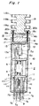
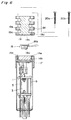
- An apparatus (photomultiplier) shown in Figs. 1 to 6 comprises a tube 1, a lid member 14a for sealing an opening AP1 of the tube 1, a gripping mechanism (holding mechanism) 12 attached to the lower surface of the lid member 14a, a cathode supporting member 5 gripped by the gripping mechanism 12, a photocathode 4 fixed to the cathode supporting member 5, an anode 30 for collecting electrons generated in the photocathode 4, and an electronic cooling element (cooler) 18 fixed to the upper surface of the lid member 14a.
- the tube 1 is comprised of a transparent material and has the opening AP1 and an opening AP2.
- the material of this tube is glass.
- the lid member 14a is comprised of a heat conductive material.
- the material of the lid member 14a is Kovar as an alloy of Fe, Ni, and Co.
- the gripping mechanism 12 is comprised of a heat conductive material.
- the gripping mechanism 12 has a pair of gripping members 13x and 13y for biasing the cathode supporting member 5 sandwiched therebetween.
- the material of the gripping members 13x and 13y is CuBe.
- the cathode supporting member 5 is comprised of a heat conductive material and arranged in the tube 1.
- the material of the cathode supporting member 5 is Al.
- the photocathode 4 emits electrons E1 and E2 in response to light LT1 incident thereon via the tube 1 (see Fig. 2).
- the anode 30 is arranged in the tube 1. By supplying power to the electronic cooling element 18, a cool portion 18a thereof is cooled and a hot portion 18b thereof is heated.
- the electronic cooling element 18 is a Peltier element.
- this apparatus further comprises a fixing member 14b, an adhesive member 16, and bolts 20a and 20b.
- the fixing member 14b is arranged between the lid member 14a and the electronic cooling element 18.
- the fixing member 14b is comprised of a material having electrically conductive and heat conductive properties and has fixing holes 14d and 14e.
- the material of the fixing member 14b is selected from any one of Cu and Al.
- the adhesive member 16 is interposed between the fixing member 14b and the lid member 14a and adheres the fixing member 14b to the lid member 14a.
- the adhesive member 16 is comprised of a material having electrically insulating and heat conductive properties.
- the material of the adhesive member 16 is an R bond resin.
- the heat sink 19 contacts the hot portion 18b of the electronic cooling element 18 and has fixing holes 19c and 19d.
- the bolts 20a and 20b are inserted in the fixing holes 14d and 14e of the fixing member 14b through the fixing holes 19c and 19d of the heat sink 19.
- the heat sink 19 is fixed to the electronic cooling element 18 via the bolts 20a and 20b.
- the fixing member 14b is comprised of a heat conductive material so that heat from the cathode supporting member 5 may efficiently conduct to the electronic cooling element 18. Most of heat conductive materials are highly electrically conductive.
- the bolts 20a and 20b are comprised of an electrically insulating material, i.e., plastic.
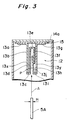
- the present apparatus further comprises a reinforcing member 17.
- the reinforcing member 17 is interposed between the lid member 14a and the fixing member 14b.
- the reinforcing member 17 has an opening AP3, an annular portion 17a having the opening AP3 in which the adhesive member 16 is arranged, and a cylindrical portion 17b, continuous with the annular portion 17a, for covering a predetermined area of an outer surface 1p of the tube 1 and a predetermined area of a circumferential surface 14p of the fixing member 14b to tighten the tube 1 and the fixing member 14b (see Fig. 5).
- the material of the reinforcing member 17 is silicone rubber.
- the gripping members 13x and 13y are comprised of a highly elastic material.
- the lid member 14a is comprised of a material having a high adhesion strength with to the glass tube 1, it is difficult to directly fix the lid member 14a to the gripping members 13x and 13y made of the highly elastic material.
- the holding mechanism 12 further comprises a buffer member 15 interposed between the gripping members 13x and 13y and the lid member 14a.
- the material of the lid member 14a is an alloy of Fe, Ni, and Co
- the material of the gripping members 13x and 13y is CuBe
- the material of the buffer member 15 is preferably Ni.
- a predetermined potential is applied to the cathode supporting member 5 via a first pin 7a during the operation of the apparatus. Since the cathode supporting member 5 is cooled, the first pin 7a connected to the cathode supporting member 5 is also cooled. When the first pin 7a is cooled, dew attaches to the first pin 7a.
- the present apparatus further comprises a wiring cable K1 for connecting the cathode supporting member 5 to the first pin 7a.
- the wiring cable K1 is longer than any one of wiring cables K2 to K7 respectively connected to remaining pins 7b to 7g. Therefore, dew is prevented from attaching to the first pin 7a even if the first pin 7a is cooled.
- the wiring cable K1 is a coiled wiring cable electrically connected to the cathode supporting member 5.
- the coiled wiring cable K1 is electrically connected to the first pin 7a.
- a detector main body 2 is arranged in the cylindrical transparent tube or glass valve 1.
- the detector main body 2 comprises the photoelectric converting unit (photocathode) 4 for generating photoelectrons in accordance with incident light via the glass valve 1 and a grid 3, the cathode supporting member or substrate 5 with good heat conductive and electrically conductive properties which has the photoelectric converting unit 4 on its surface, a plurality of stages of dynodes 6a, 6b, 6c, 6d, 6e, 6f, 6g, 6h, and 6i for sequentially multiplying the photoelectrons emitted from the photoelectric converting unit 4, i.e., the photoelectric surface, and the anode 30 for collecting the multiplied photoelectrons to extract them as an output signal.
- the detector main body 2 has the first pin 7a for applying a predetermined potential to the grid 3 and the photocathode 4, the pair of pins 7a and 7e for applying a voltage across the photocathode 4 and the first stage dynode 6a, the pair of pins 7e and 7c for applying a voltage across the first stage dynode 6a and the anode 30, and the plurality of pins 7b, 7d, 7f, and 7g for applying a voltage across the remaining dynodes. A high voltage is sequentially applied across these pins.
- the detector main body 2 further comprises a stem 8 for fixing these pins or pin terminals 7, and a tubular portion 9 extending through the stem 8.
- the pin terminal 7a coupled to the substrate 5 is set to a very low temperature.
- the wiring cable K1 for preventing dew is provided midway along a connection L1 between the pin terminal 7a and the substrate 5.
- the photoelectric converting unit 4 as the photoelectric surface deposited on the substrate 5 serving as a cathode plate.
- Part or all of the cathode plate having a surface on which the photoelectric surface (photoelectric converting unit) 4 is deposited may be adhered to a shield plate.
- a composite of the shield plate and the cathode plate functions as the substrate 5.
- the substrate 5 projects from first and second insulating substrates 10 and 11, and particularly a projection amount is larger on the first insulating substrate 10 side.
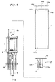
- the substrate 5 has a wide joining piece 5a at its top portion.
- the gripping members or contact pieces 13x and 13y of the gripping mechanism or contact member 12 are joined to the joining piece 5a.
- the contact pieces 13x and 13y are fixed to the lid member or conductive plate 14a which constitutes part of the heat conductor (14a, 16, and 14b), and project toward the substrate 5. As shown in Figs.
- the contact member 12 (holding mechanism, or gripping mechanism) has the contact pieces 13x and 13y each of which is comprised of a CuBe material having spring elasticity and has a plate thickness of about 0.3 mm and a plate width of about 5 mm, and the buffer member or holder plate 15 for fixing the contact pieces 13x and 13y by electronic welding or the like.
- the first contact piece 13x comprises a first leg portion 13a fixed to the holder plate 15, a first elastic portion 13b extending from one end of the first leg portion 13a at a right angle, a second elastic portion 13d extending inward from the first elastic portion 13b via a first bent portion 13c having a bending angle of 90°, and a third elastic portion 13f extending inward from the second elastic portion 13d via a second bent portion 13e having a bending angle of 90°.
- the second contact piece 13y comprises a second leg portion 13g fixed to the holder plate 15, a fourth elastic portion 13h extending from one end of the second leg portion 13g at a right angle, and a fifth elastic portion 13j extending inward from the fourth elastic portion 13h via a third bent portion 13i having a bending angle of 90°.
- an accommodation portion P for accommodating the joining piece 5a of the substrate 5 is constituted by the second elastic portion 13d, the second bent portion 13e, the third elastic portion 13f, and the fifth elastic portion 13j.
- the center of the accommodation portion P becomes narrower than a plate thickness H of the joining piece 5a due to the overlap of the third elastic portion 13f and the fifth elastic portion 13j.
- the joining piece 5a of the substrate 5 is elastically sandwiched in the accommodation portion P by the cooperation of the first and second contact pieces 13x and 13y to be brought into surface contact with the contact pieces 13x and 13y. Therefore, by the assembling operation of inserting the detector main body 2 in the glass valve 1, the substrate 5 can be coupled to the heat conductor 14 via the contact pieces 13x and 13y at once.
- the heat conductor 14 is constituted by the lid member or Kovar metal-made conductive plate 14a which is fused to the glass valve 1 by RF heating so as to close the opening end of the glass valve 1, and the fixing member or base 14b which is adhered to the conductive plate 14a via the resin adhesive (preferably R bond; tradename) 16 having good heat conductive and electrically insulating properties and is comprised of a Cu or Al material.
- the reinforcing member or cylindrical ring 17 made of silicone rubber is attached to the outer surface of the top portion of the glass valve 1 and has a shape to accommodate the heat conductor 14. Therefore, by using the ring 17, dew can be prevented at the top portion of the glass valve 1, and the number of manufacturing steps can be decreased. That is, by using the ring 17, the adhesive 16 can be prevented from flowing out, and positioning of the heat conductor 14 can be assured.
- the cool portion or low-temperature plate 18a at a low temperature side of the Peltier element 18 which constitutes part of a cooling device 21 is directly fixed on the base 14b.
- the heat sink 19 having radiation fins 119a to 119c which constitutes part of the cooling device 21 is fixed to the hot portion or high-temperature plate 18b at the high temperature side of the Peltier element 18.
- the Peltier element 18 comprises, between the low-temperature plate 18a and the high-temperature plate 18b, a thermoelectric cooling portion 18c for dissipating, by an applied voltage, heat absorbed by the high-temperature plate 18b from the low-temperature plate 18a.
- the Peltier element 18 is clamped between the base 14b and the heat sink 19 by the pair of bolts or screws 20a and 20b made of a plastic. One end of each of the screws 20a and 20b is fastened in the base 14b, and the other end is fixed to the heat sink 19.
- a predetermined potential is applied to the photocathode 4, the dynodes 6a to 6i, and the anode 30 of the detector main body 2 via the pin terminals 7a to 7g.
- photoelectrons are generated from the photoelectric converting unit 4, i.e., the photoelectric surface in accordance with incident light.
- the photoelectrons are sequentially multiplied by the plurality of dynodes 6a to 6i, and the multiplied photoelectrons are collected by the anode 30 as an output signal.
- Unnecessary thermoelectrons are emitted from the photoelectric converting unit 4, i.e., the photoelectric surface due to heat of the photoelectric surface.
- the photoelectric converting unit 4 is continuously cooled by the Peltier effect while heat of the photoelectric converting unit 4 is absorbed by the high-temperature plate 18b of the Peltier element 18 from the low-temperature plate 18a via the contact pieces 13x and 13y joined to the substrate 5. Therefore, generation of thermoelectrons from the photoelectric surface 4 can be reduced.
- This manufacturing method comprises the step of sealing one opening AP1 of the glass tube 1 by the heat conductive member 14a, the step of attaching, to a lower surface 14c of the heat conductive member 14a, the pair of gripping members 13x and 13y which extend from the heat conductive member 14a to the other opening AP2 of the glass tube 1 and oppose each other at a predetermined interval, the step of inserting the cathode supporting member 5 between the gripping members 13x and 13y from the other opening AP2 of the glass tube 1 to attach the cathode supporting member 5 to the heat conductive member 14a, the step of attaching the electronic cooling element 18 to an upper surface 14u of the heat conductive member 14a, and the step of forming the photocathode 4 on a surface 5s of the cathode supporting member 5.
- the conductive plate 14a constituting part of the heat conductor 14 is fused by RF heating to one end of the glass valve 1 whose two ends are open.
- the holder plate 15 of the contact member 12 is fixed to the lower surface or inner surface 14c of the conductive plate 14a by electronic welding.
- the detector main body 2 is inserted from the other end of the glass valve 1
- the joining piece 5a of the substrate 5 is pressed into the accommodation portion P of the contact pieces 13.
- the joining piece 5a of the substrate 5 is elastically sandwiched in the accommodation portion P by the cooperation of the first contact piece 13x and the second contact piece 13y to surface-contact the contact pieces 13.
- the glass valve 1 and the stem 8 are fused by using an oxygen burner or the like.
- the glass valve 1 is sealed by the conductive plate 14a and the stem 8.
- the interior of the glass valve 1 is evacuated via the tubular portion 9 in a direction of an arrow B to set the interior of the glass valve 1 at 10 ⁇ 8 torr.
- Sb is deposited on the photoelectric converting unit 4 and the dynodes 6 in advance.
- an alkali is activated in the glass valve 1.
- the end portion of the tubular portion 9 is closed to completely seal the glass valve 1.
- the ring 17 made of silicone rubber is fitted in the glass valve 1 to bring the annular portion or pawl portion 17a of the ring 17 into contact with the conductive plate 14a.
- the resin adhesive (preferably R bond; tradename) 16 having good heat conductive and electrically insulating properties is poured into a space 17s formed by the pawl portion 17a and the conductive plate 14a.
- the base 14b is inserted in the ring 17 from the upper portion to fix the base 14b to the conductive plate 14a via the adhesive 16 and the pawl portion 17a.
- the assembling operation of the heat conductor 14 is finished. Note that the base 14b must be tightly pressed so as not to form a gap between the adhesive 16 and the base 14b.
- the adhesive 16 solidifies to firmly fix the base 14b to the conductive plate 14a.
- the low-temperature plate 18a of the Peltier element 18 is brought into contact with the base 14b, and an end face 19b of the heat sink 19 is brought into contact with the high-temperature plate 18b of the Peltier element 18.
- the two screws 20 are threadably engaged with the fixing holes or male thread portions 14d and 14e of the base 14b by inserting the screws 20 into the fixing holes or through holes 19c and 19d.
- the cooling device 21 is properly positioned with respect to the heat conductor 14.
- the photoelectric detector of the present invention is not limited to the above embodiment.
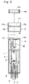
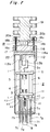
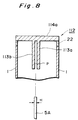
- a cathode supporting member 5 may be sandwiched by a ceramic member 112. That is, an apparatus shown in Figs. 7 and 8 comprises a tube 1, the ceramic member 112, the cathode supporting member 5, a photocathode 4, an anode shown in Fig. 2, a metal seal member 22, and an electronic cooling element 18. Note that the same reference numerals as in Fig. 1 denote the same parts in the apparatus shown in Figs. 7 and 8.
- the ceramic member 112 comprises a lid portion or member 114a for sealing the opening of the tube 1, and a pair of gripping portions 113a and 113b, continuous with the lid portion 114a, for sandwiching the cathode supporting member 5 therebetween. Since the cathode supporitng member 5 and the ceramic member 112 are comprised of heat conductive materials, the photocathode 4 fixed to the cathode supporting member 5 is cooled by the electronic cooling element 18 via the cathode supporting member 5, the ceramic member 112, an adhesive member 116, and a fixing member 14b. Since a ceramic is an electrical insulator, the adhesive member 116 need not be an electrical insulator.
- Electrons emitted from the cooled photocathode 4 are collected by an anode 30 arranged in the tube, as shown in Fig. 2.
- the metal seal member 22 is interposed between the ceramic member 112 and the tube 1.
- the metal seal member 22 is comprised of an alloy of Fe, Ni, and Co.
- the lid portion 114a and the gripping portions 113a and 113b are integrally formed of a ceramic.
- the ceramic member or gripping mechanism 112 comprises the two gripping portions or first and second linear contact pieces 113a and 113b which are disposed parallel to each other.
- the ceramic member 112 has an accommodation space P having a width slightly smaller than a plate thickness H of the joining piece 5a. Therefore, when the joining piece or one end portion 5a of the cathode supporting member is inserted between the gripping portions 113a and 113b, the gripping portions 113a and 113b bias and hold the joining piece 5a sandwiched therebetween.
- the contact pieces 113a and 113b can be easily positioned in the glass valve 1.
- the joining piece 5a can be elastically clamped between the first and second contact pieces 113a and 113b.
- the ceramic member or ceramic heat conductor 112 and the glass valve 1 are fixed to each other via the appropriate metal member 22 to firmly join them.
- the effect of integrally forming the lid member 114a and the contact pieces 113a and 113b by using a ceramic is as follows: an electrically insulating member need not be provided between the electronic cooling element or Peltier element 18 and the lid member 114a because a ceramic itself has an electrically insulating property, thereby improving the heat conductivity.
- a method of manufacturing this photoelectric detecting tube comprises the step of sealing one opening AP of the glass tube 1 by the ceramic member 112, the step of inserting the cathode supporting member 5 between the pair of opposite gripping members 113a and 113b of the ceramic member 112 from the other opening of the glass tube 1 to attach the cathode supporting member 5 to the ceramic member 112, the step of attaching the electronic cooling element 18 to the ceramic member 112, and the step of forming the photocathode 4 on the surface of the cathode supporting member 5.
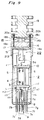
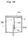
- an apparatus can be constituted such that one elastic contact piece 213 biases a joining piece 5a without employing the above-mentioned arrangement in which the contact pieces 113a and 113b clamp the joining piece 5a.
- a holding mechanism 212 comprises the contact piece or biasing member 213 bent at an acute angle, and a buffer member 15 to which one end of the biasing member 213 is fixed.
- the biasing member 213 biases one end portion 5a of a cathode supporting member 5 while a projecting portion 213p of the contact piece 213 contacts one end portion 5a.
- the same reference numerals as in Fig. 1 denote the same parts in the apparatus shown in Figs. 9 and 10.
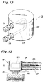
- a heat sink 19 may be of a water cooling type.
- the heat sink 19 may be constituted such that a flow path 23 is formed in a solid heat sink main body 22 with good heat conductive properties, which has a cylindrical or rectangular parallelepiped shape, and mouthpiece portions 24 and 25 are respectively formed at the outlet and inlet sides of the flow path 23.
- These mouthpiece portions 24 and 25 are coupled to a pump (not shown) as a fluid generating source for feeding a stream of 200 to 300 cc/min. Therefore, by employing the water cooling type heat sink 19, the Peltier effect of a Peltier element 18 can be maximized.
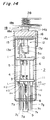
- the same reference numerals as in Fig. 1 denote the same parts in the apparatus shown in Figs. 11 to 13.
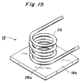
- a tubular portion-shaped heat sink main body 28 having good heat conductive properties may be constituted spirally, and an end face 28a of the heat sink main body 28 may contact a high-temperature plate 18b of a Peltier element 18 to be fixed thereto.
- the same reference numerals as in Fig. 1 denote the same parts in the apparatus shown in Figs. 14 and 15.
- a photoelectric detector with a cooling device and a manufacturing method thereof according to the present invention are constituted as described above. Therefore, the following effects can be obtained.
- the detector main body can be reliably joined and mounted to the cooling device.
- the assembling operation of the detector main body and the cooling device can be facilitated.
Landscapes
- Photometry And Measurement Of Optical Pulse Characteristics (AREA)
- Manufacture Of Electron Tubes, Discharge Lamp Vessels, Lead-In Wires, And The Like (AREA)
Applications Claiming Priority (3)
| Application Number | Priority Date | Filing Date | Title |
|---|---|---|---|
| JP14820094A JP3455588B2 (ja) | 1994-06-29 | 1994-06-29 | 冷却装置付き光電検出器及びその製造方法 |
| JP14820094 | 1994-06-29 | ||
| JP148200/94 | 1994-06-29 |
Publications (3)
| Publication Number | Publication Date |
|---|---|
| EP0690477A2 true EP0690477A2 (de) | 1996-01-03 |
| EP0690477A3 EP0690477A3 (de) | 1997-12-29 |
| EP0690477B1 EP0690477B1 (de) | 2003-03-19 |
Family
ID=15447503
Family Applications (1)
| Application Number | Title | Priority Date | Filing Date |
|---|---|---|---|
| EP95304586A Expired - Lifetime EP0690477B1 (de) | 1994-06-29 | 1995-06-29 | Photodetektorröhre mit Kühler |
Country Status (4)
| Country | Link |
|---|---|
| US (2) | US5719390A (de) |
| EP (1) | EP0690477B1 (de) |
| JP (1) | JP3455588B2 (de) |
| DE (1) | DE69529943T2 (de) |
Families Citing this family (10)
| Publication number | Priority date | Publication date | Assignee | Title |
|---|---|---|---|---|
| JP3455588B2 (ja) * | 1994-06-29 | 2003-10-14 | 浜松ホトニクス株式会社 | 冷却装置付き光電検出器及びその製造方法 |
| KR100494264B1 (ko) | 1997-11-19 | 2005-06-13 | 하마마츠 포토닉스 가부시키가이샤 | 광 검출 장치 및 이것을 사용한 촬상 장치 |
| JP4128654B2 (ja) * | 1998-05-13 | 2008-07-30 | 浜松ホトニクス株式会社 | 電子管装置 |
| US6312617B1 (en) * | 1998-10-13 | 2001-11-06 | Board Of Trustees Operating Michigan State University | Conductive isostructural compounds |
| US6545256B1 (en) * | 2000-04-20 | 2003-04-08 | Hamamatsu Photonics K.K. | Light receiving module and radiation detecting apparatus equipped with the same |
| JP2007505028A (ja) * | 2003-09-12 | 2007-03-08 | ボード オブ トラスティース オペレイティング ミシガン ステイト ユニバーシティー | 銀を含有する熱電気的な合成物 |
| US8481843B2 (en) * | 2003-09-12 | 2013-07-09 | Board Of Trustees Operating Michigan State University | Silver-containing p-type semiconductor |
| CN1317592C (zh) * | 2004-07-19 | 2007-05-23 | 友达光电股份有限公司 | 散热固定装置及其散热方法 |
| US9892893B2 (en) * | 2015-03-23 | 2018-02-13 | Molecular Devices, Llc | Cooled photomultiplier tube based light detector with reduced condensation, and related apparatuses and methods |
| JP6508140B2 (ja) * | 2016-06-30 | 2019-05-08 | 東亜ディーケーケー株式会社 | 光電子増倍管、測定装置、製造用治具 |
Citations (2)
| Publication number | Priority date | Publication date | Assignee | Title |
|---|---|---|---|---|
| JPS49106380A (de) | 1973-01-19 | 1974-10-08 | ||
| JPH06148200A (ja) | 1992-11-11 | 1994-05-27 | Nittec Co Ltd | 免疫自動分析装置 |
Family Cites Families (6)
| Publication number | Priority date | Publication date | Assignee | Title |
|---|---|---|---|---|
| US3757151A (en) * | 1972-08-11 | 1973-09-04 | Ace Sophisticates Inc | Internal cooling for photodetectors |
| US4024390A (en) * | 1976-04-09 | 1977-05-17 | The United States Of America As Represented By The Secretary Of The Army | Two microchannel plate picture element array image intensifier tube and system |
| JPH0584016A (ja) * | 1991-09-27 | 1993-04-06 | Iseki & Co Ltd | コンバインの脱穀変速制御装置 |
| JP2662341B2 (ja) * | 1992-05-20 | 1997-10-08 | 浜松ホトニクス株式会社 | 電子増倍管 |
| US5343360A (en) * | 1993-03-31 | 1994-08-30 | Ncr Corporation | Containing and cooling apparatus for an integrated circuit device having a thermal insulator |
| JP3455588B2 (ja) * | 1994-06-29 | 2003-10-14 | 浜松ホトニクス株式会社 | 冷却装置付き光電検出器及びその製造方法 |
-
1994
- 1994-06-29 JP JP14820094A patent/JP3455588B2/ja not_active Expired - Fee Related
-
1995
- 1995-06-29 EP EP95304586A patent/EP0690477B1/de not_active Expired - Lifetime
- 1995-06-29 DE DE69529943T patent/DE69529943T2/de not_active Expired - Fee Related
- 1995-06-29 US US08/496,647 patent/US5719390A/en not_active Expired - Fee Related
-
1997
- 1997-07-29 US US08/902,329 patent/US5886341A/en not_active Expired - Fee Related
Patent Citations (2)
| Publication number | Priority date | Publication date | Assignee | Title |
|---|---|---|---|---|
| JPS49106380A (de) | 1973-01-19 | 1974-10-08 | ||
| JPH06148200A (ja) | 1992-11-11 | 1994-05-27 | Nittec Co Ltd | 免疫自動分析装置 |
Also Published As
| Publication number | Publication date |
|---|---|
| US5719390A (en) | 1998-02-17 |
| EP0690477B1 (de) | 2003-03-19 |
| DE69529943T2 (de) | 2004-01-08 |
| JP3455588B2 (ja) | 2003-10-14 |
| DE69529943D1 (de) | 2003-04-24 |
| US5886341A (en) | 1999-03-23 |
| EP0690477A3 (de) | 1997-12-29 |
| JPH0817390A (ja) | 1996-01-19 |
Similar Documents
| Publication | Publication Date | Title |
|---|---|---|
| US5886341A (en) | Photodetection tube with a slidably adapted cathode substrate | |
| JP4237411B2 (ja) | ガス放電管 | |
| US5587625A (en) | Gas discharge tube | |
| JP2784148B2 (ja) | ガス放電管 | |
| KR102092368B1 (ko) | 엑스레이 튜브 및 이의 제조방법 | |
| EP0820089A1 (de) | Elektronenröhre | |
| US8115386B2 (en) | Photomultiplier tube | |
| US20070023617A1 (en) | Low cost planar image intensifier tube structure | |
| US6765352B2 (en) | Photocathode and electron tube | |
| US6407500B1 (en) | Electrode structure in flat vacuum envelope | |
| US7176625B2 (en) | Photocathode plate and electron tube | |
| US7002132B2 (en) | Photocathode, electron tube, and method of assembling photocathode | |
| EP0860857B1 (de) | Elektronenröhre | |
| US6198221B1 (en) | Electron tube | |
| JP4390346B2 (ja) | 光源装置 | |
| JPH11329338A (ja) | 電子管装置 | |
| JPS5841618B2 (ja) | 電子放電装置 | |
| WO2003005408A1 (en) | Electron tube and method of manufacturing the electron tube | |
| JP4192619B2 (ja) | 発光ダイオードランプ装置 | |
| US6531821B1 (en) | Gas discharge tube | |
| US6852979B1 (en) | Photomultiplier tube, photomultiplier tube unit, radiation detector | |
| JPH1167145A (ja) | 冷却型光電子増倍管 | |
| JP7360975B2 (ja) | 光検出器 | |
| JPH1012183A (ja) | 冷却装置付き光電検出器及びその製造方法 | |
| JPH1167144A (ja) | 冷却型光電子増倍管 |
Legal Events
| Date | Code | Title | Description |
|---|---|---|---|
| PUAI | Public reference made under article 153(3) epc to a published international application that has entered the european phase |
Free format text: ORIGINAL CODE: 0009012 |
|
| AK | Designated contracting states |
Kind code of ref document: A2 Designated state(s): DE FR GB NL SE |
|
| PUAL | Search report despatched |
Free format text: ORIGINAL CODE: 0009013 |
|
| AK | Designated contracting states |
Kind code of ref document: A3 Designated state(s): DE FR GB NL SE |
|
| 17P | Request for examination filed |
Effective date: 19980623 |
|
| 17Q | First examination report despatched |
Effective date: 19981113 |
|
| GRAG | Despatch of communication of intention to grant |
Free format text: ORIGINAL CODE: EPIDOS AGRA |
|
| GRAG | Despatch of communication of intention to grant |
Free format text: ORIGINAL CODE: EPIDOS AGRA |
|
| GRAH | Despatch of communication of intention to grant a patent |
Free format text: ORIGINAL CODE: EPIDOS IGRA |
|
| GRAH | Despatch of communication of intention to grant a patent |
Free format text: ORIGINAL CODE: EPIDOS IGRA |
|
| GRAA | (expected) grant |
Free format text: ORIGINAL CODE: 0009210 |
|
| AK | Designated contracting states |
Designated state(s): DE FR GB NL SE |
|
| PG25 | Lapsed in a contracting state [announced via postgrant information from national office to epo] |
Ref country code: NL Free format text: LAPSE BECAUSE OF FAILURE TO SUBMIT A TRANSLATION OF THE DESCRIPTION OR TO PAY THE FEE WITHIN THE PRESCRIBED TIME-LIMIT Effective date: 20030319 |
|
| REG | Reference to a national code |
Ref country code: GB Ref legal event code: FG4D |
|
| REF | Corresponds to: |
Ref document number: 69529943 Country of ref document: DE Date of ref document: 20030424 Kind code of ref document: P |
|
| PG25 | Lapsed in a contracting state [announced via postgrant information from national office to epo] |
Ref country code: SE Free format text: LAPSE BECAUSE OF FAILURE TO SUBMIT A TRANSLATION OF THE DESCRIPTION OR TO PAY THE FEE WITHIN THE PRESCRIBED TIME-LIMIT Effective date: 20030619 |
|
| ET | Fr: translation filed | ||
| NLV1 | Nl: lapsed or annulled due to failure to fulfill the requirements of art. 29p and 29m of the patents act | ||
| PLBE | No opposition filed within time limit |
Free format text: ORIGINAL CODE: 0009261 |
|
| STAA | Information on the status of an ep patent application or granted ep patent |
Free format text: STATUS: NO OPPOSITION FILED WITHIN TIME LIMIT |
|
| 26N | No opposition filed |
Effective date: 20031222 |
|
| PGFP | Annual fee paid to national office [announced via postgrant information from national office to epo] |
Ref country code: DE Payment date: 20070621 Year of fee payment: 13 |
|
| PGFP | Annual fee paid to national office [announced via postgrant information from national office to epo] |
Ref country code: GB Payment date: 20070627 Year of fee payment: 13 |
|
| PGFP | Annual fee paid to national office [announced via postgrant information from national office to epo] |
Ref country code: FR Payment date: 20070608 Year of fee payment: 13 |
|
| GBPC | Gb: european patent ceased through non-payment of renewal fee |
Effective date: 20080629 |
|
| REG | Reference to a national code |
Ref country code: FR Ref legal event code: ST Effective date: 20090228 |
|
| PG25 | Lapsed in a contracting state [announced via postgrant information from national office to epo] |
Ref country code: DE Free format text: LAPSE BECAUSE OF NON-PAYMENT OF DUE FEES Effective date: 20090101 |
|
| PG25 | Lapsed in a contracting state [announced via postgrant information from national office to epo] |
Ref country code: GB Free format text: LAPSE BECAUSE OF NON-PAYMENT OF DUE FEES Effective date: 20080629 |
|
| PG25 | Lapsed in a contracting state [announced via postgrant information from national office to epo] |
Ref country code: FR Free format text: LAPSE BECAUSE OF NON-PAYMENT OF DUE FEES Effective date: 20080630 |