EP0689315A1 - Phasenkomparator - Google Patents
Phasenkomparator Download PDFInfo
- Publication number
- EP0689315A1 EP0689315A1 EP95401435A EP95401435A EP0689315A1 EP 0689315 A1 EP0689315 A1 EP 0689315A1 EP 95401435 A EP95401435 A EP 95401435A EP 95401435 A EP95401435 A EP 95401435A EP 0689315 A1 EP0689315 A1 EP 0689315A1
- Authority
- EP
- European Patent Office
- Prior art keywords
- signal
- digital signal
- circuit
- input
- pulse
- Prior art date
- Legal status (The legal status is an assumption and is not a legal conclusion. Google has not performed a legal analysis and makes no representation as to the accuracy of the status listed.)
- Granted
Links
- 230000003111 delayed effect Effects 0.000 claims abstract description 43
- 230000007704 transition Effects 0.000 claims abstract description 25
- 238000001514 detection method Methods 0.000 claims abstract description 19
- 230000010363 phase shift Effects 0.000 claims abstract description 15
- 230000001360 synchronised effect Effects 0.000 claims description 38
- 230000000630 rising effect Effects 0.000 claims description 8
- 238000004364 calculation method Methods 0.000 claims description 2
- 230000005540 biological transmission Effects 0.000 description 8
- 238000010586 diagram Methods 0.000 description 6
- 230000006870 function Effects 0.000 description 4
- 238000012545 processing Methods 0.000 description 4
- 238000011084 recovery Methods 0.000 description 4
- 235000021183 entrée Nutrition 0.000 description 2
- 238000004519 manufacturing process Methods 0.000 description 2
- 238000000034 method Methods 0.000 description 2
- 230000033764 rhythmic process Effects 0.000 description 2
- 230000003068 static effect Effects 0.000 description 2
- 238000004458 analytical method Methods 0.000 description 1
- 238000012937 correction Methods 0.000 description 1
- 239000013078 crystal Substances 0.000 description 1
- 230000001627 detrimental effect Effects 0.000 description 1
- 230000000694 effects Effects 0.000 description 1
- 238000005516 engineering process Methods 0.000 description 1
- 238000001914 filtration Methods 0.000 description 1
- 230000010354 integration Effects 0.000 description 1
- 238000012423 maintenance Methods 0.000 description 1
- 238000005259 measurement Methods 0.000 description 1
- 230000008929 regeneration Effects 0.000 description 1
- 238000011069 regeneration method Methods 0.000 description 1
- 230000000717 retained effect Effects 0.000 description 1
- 238000007493 shaping process Methods 0.000 description 1
- 239000000758 substrate Substances 0.000 description 1
Images


Classifications
-
- H—ELECTRICITY
- H03—ELECTRONIC CIRCUITRY
- H03L—AUTOMATIC CONTROL, STARTING, SYNCHRONISATION, OR STABILISATION OF GENERATORS OF ELECTRONIC OSCILLATIONS OR PULSES
- H03L7/00—Automatic control of frequency or phase; Synchronisation
- H03L7/06—Automatic control of frequency or phase; Synchronisation using a reference signal applied to a frequency- or phase-locked loop
- H03L7/08—Details of the phase-locked loop
- H03L7/085—Details of the phase-locked loop concerning mainly the frequency- or phase-detection arrangement including the filtering or amplification of its output signal
- H03L7/089—Details of the phase-locked loop concerning mainly the frequency- or phase-detection arrangement including the filtering or amplification of its output signal the phase or frequency detector generating up-down pulses
-
- H—ELECTRICITY
- H03—ELECTRONIC CIRCUITRY
- H03D—DEMODULATION OR TRANSFERENCE OF MODULATION FROM ONE CARRIER TO ANOTHER
- H03D13/00—Circuits for comparing the phase or frequency of two mutually-independent oscillations
- H03D13/003—Circuits for comparing the phase or frequency of two mutually-independent oscillations in which both oscillations are converted by logic means into pulses which are applied to filtering or integrating means
- H03D13/004—Circuits for comparing the phase or frequency of two mutually-independent oscillations in which both oscillations are converted by logic means into pulses which are applied to filtering or integrating means the logic means delivering pulses at more than one terminal, e.g. up and down pulses
-
- H—ELECTRICITY
- H04—ELECTRIC COMMUNICATION TECHNIQUE
- H04L—TRANSMISSION OF DIGITAL INFORMATION, e.g. TELEGRAPHIC COMMUNICATION
- H04L7/00—Arrangements for synchronising receiver with transmitter
- H04L7/02—Speed or phase control by the received code signals, the signals containing no special synchronisation information
- H04L7/033—Speed or phase control by the received code signals, the signals containing no special synchronisation information using the transitions of the received signal to control the phase of the synchronising-signal-generating means, e.g. using a phase-locked loop
Definitions
- the improvement of the performances of these latter circuits consists, according to current techniques, either of reducing the effects of the different noise sources, in particular of phase noise, present in these circuits, in order to improve the performances relative to the phenomenon of " jitter "known under the name of” jitter “in Anglo-Saxon terms, that is to minimize transmission errors by improving the noise tolerance of the timing recovery circuit.
- This last operation is carried out during the resynchronization of the digital data, constituted by a series of binary elements, by means of a flip-flop synchronized with the reference clock signal and by maintaining the active edge of the clock signal in middle of each bit.
- Such a measurement implies perfect synchronization of the active edge of the clock signal and the half-period of the bit stream.
- the aforementioned signal to be integrated, or differential signal therefore has a significant peak-to-peak amplitude and a maximum frequency equal to the binary element frequency or bit frequency.
- Such a signal is likely to constitute a very significant source of " jitter " in the circuit, unless a very careful filtering treatment is provided.
- the above-mentioned " jitter " phenomenon can therefore prove to be very annoying, in particular in transmission devices constituted by successive elements in cascade, for which it is well known that the " jitter " phenomenon accumulates and systematically increases along the chain of transmission.
- the present invention relates to the implementation of a phase comparator device retaining the advantages obtained by the circuit described in the aforementioned article while eliminating or substantially reducing its contribution to the phenomenon of " jitter ".
- the device for comparing the phase between transitions of a digital signal formed by a series of bits ⁇ ak ⁇ and a clock signal Ck at the frequency binary element of this digital signal is remarkable in that it comprises a first detection channel making it possible, from the clock signal Ck and the digital signal, to generate a digital signal delayed by a delay value ⁇ , 0 ⁇ ⁇ T, where T denotes the period of the signal digital, this first detection channel further comprising a generator circuit at each transition of a first pulse whose duration is variable, proportional to the phase shift between the digital signal delayed and the clock signal.
- a second detection channel which makes it possible, from the clock signal and the digital signal, to generate at each transition of the digital signal a second pulse of constant duration equal to the half-period of the clock signal.
- a circuit for calculating the average value, over at least one cycle of the clock signal, of the algebraic difference between the first and the second pulse delivers a phase comparison signal between digital signal and clock signal of zero value for zero phase shift and exact centering of the pulse formed by two consecutive transitions of the digital signal delayed on a rising or falling edge of the clock signal and of positive or negative value for a phase shift of the signal signal delay respectively clock versus delayed digital signal.
- phase comparator device object of the present invention, finds application in the production of electronic circuits for processing digital signals, in particular in the form of integrated circuits.
- phase comparator device between transitions of a digital signal, object of the present invention, will now be given in connection with FIG. 2a.
- the digital signal is a data signal, referenced by the letter D, formed by a series of bits or binary elements, denoted ⁇ ak ⁇ .
- a clock signal denoted Ck
- this clock signal being a signal at the bit frequency or binary element frequency of the aforementioned digital signal, deemed to have a period corresponding to the duration of each bit, designated by T.
- the phase comparator device object of the present invention, comprises a first detection channel, denoted 1, allowing, from the clock signal Ck and the signal digital D, to generate a delayed digital signal, noted DR, with a delay value ⁇ between 0 ⁇ ⁇ T.
- the delayed digital signal DR can be generated via a delay circuit 10, which will be described in more detail later in the description.
- the first channel 1 further comprises a circuit 11 generator at each transition of the digital signal D of a first pulse whose duration is variable, proportional to the phase shift between the delayed digital signal DR and the clock signal Ck.
- This signal is denoted S1 in FIG. 2a, the output of the generator circuit 11 constituting in fact the output of the first detection channel 1 previously mentioned.
- the comparator device further comprises a second detection channel, denoted 2, making it possible, from the clock signal Ck and the digital signal D, to generate at each transition of the above-mentioned digital signal, a second calibrated pulse of constant duration, equal to the half-period of the clock signal Ck.
- the second calibrated pulse is denoted Sp in FIG. 2a.
- a circuit 3 for calculating the average value of the difference between the first and the second pulse is provided, this calculation circuit 3 delivering a phase comparison signal V0 between delayed digital signal DR and clock signal of zero value for zero phase shift and exact centering of the pulse formed by two consecutive transitions of the delayed digital signal DR on a rising or falling edge of the clock signal.
- the phase comparison signal V0 has, on the contrary, a positive mean value, respectively negative, for a phase shift of advance respectively of delay of the clock signal Ck with respect to the aforementioned delayed digital signal DR.
- the first detection channel 1 comprises, connected in cascade, the delay circuit 10 making it possible to introduce the delay value ⁇ under the conditions mentioned above on the digital input signal D to generate the delayed digital signal DR, and the circuit 11 generating the first pulse S1.
- the delay circuit 10 can be produced either by a so-called external circuit, that is to say by a circuit of the analog delay line type, or, on the contrary, by an internal circuit when the delay circuit 10 is produced for example by means of successive logic gates, each causing an elementary delay of determined value.
- the delay circuit 10 is said to be internal due to the fact that the logic gates constituting the latter can be integrated on the same substrate to produce the phase comparator device, object of the present invention, such as shown in Figure 2a.
- the first detection channel 1 comprises the circuit 11 generating the first pulse S1, this circuit comprising for example a first logic circuit 111 of the exclusive OR type, receiving on a first input the delayed digital signal DR, and a flip-flop flip-flop synchronized, denoted 110, this flip-flop being synchronized with the clock signal Ck.
- the synchronized bistable flip-flop 110 receives on its clock input the clock signal Ck, on its input D the delayed digital signal DR, and delivers at its output Q a synchronized delayed digital signal, noted D1, which is directly delivered at the second input of the first logic circuit of the exclusive OR type 111. The latter delivers the first pulse S1 at the output of the first detection channel 1.
- the second detection channel 2 comprises, connected in cascade, a circuit 20 generating a digital signal offset by half a period with respect to the delayed digital signal synchronized with from the digital input signal D.
- a generator circuit At the output of the generator circuit 20, is connected a generator circuit, from the digital signal delayed by half a period delivered by the generator circuit 20, of the second pulse S p , this generator circuit of the second pulse bearing the reference 21 comprising, similarly to circuit 11 of the first channel, a second logic circuit of the exclusive OR type, denoted 211, receiving on a first input the digital signal shifted by half a period, signal denoted D2, and a synchronized bistable flip-flop, noted 210, this flip-flop being synchronized with the clock signal Ck.
- the flip-flop 210 receives on its input D the logic signal shifted by half a period, denoted D2, and on its clock input, the aforementioned signal Ck.
- the output Q of the second synchronized bistable flip-flop 210 delivers a signal D3 to a second input of the second exclusive OR gate 211.
- the generator circuit 20 of the digital signal shifted by half a period D2 with respect to the synchronized delayed digital signal can be formed by a bistable latch synchronized with the complemented clock signal. Ck ⁇ .
- the aforementioned synchronized flip-flop receives on its input D the digital input signal D, and on its clock input the complemented digital signal Ck ⁇ , and delivers on its output Q the digital signal shifted by half a period, denoted D2.
- FIG. 2b clock in phase advance.
- the chronogram represented corresponds to the case where the clock Ck is in phase advance with respect to the center of the two successive transitions, representative for example of the transmission of binary elements of successive values 0, 1, 0.
- the rising edge of the clock signal considered to be the active edge, has a phase advance ⁇ ⁇ O relative to the center of the pulse formed by the two aforementioned transitions.
- the signal D2, delivered by the flip-flop synchronized 20 on the complemented clock signal Ck ⁇ , is delayed with respect to the signal D1, the signal D2 being delivered by the synchronized flip-flop 20 for the value 1 of the complemented clock signal Ck ⁇ , that is to say the value O of the clock signal Ck.
- the average value of the second pulse S p is greater than the average value of the first pulse S1 due to the negative phase shift ⁇ , represented between the delayed digital signal DR and the clock signal Ck.
- the first pulse S1 delivered by the first exclusive OR circuit 111 has the value, for each of the transitions of the digital input signal D and therefore of the delayed digital signal DR, the offset between the rising edges of the delayed digital signal DR and of the signal D1, respectively between the falling edges of these two same signals, as shown in Figure 2b. Under these conditions, the average value of the difference S1 - S p , algebraic difference of the first and the second pulse, the second pulse always having for value the half-period T / 2, is therefore negative.
- the signal D2 delivered by the synchronized flip-flop 20 is half a period T / 2 ahead of the signal D1 delivered by the flip-flop 110.
- the signal D1 delivered by the aforementioned synchronized flip-flop 110 is more than half a period behind the delayed digital signal DR, ⁇ > 0, and the signal S1 result of the exclusive OR between these two signals therefore has a duration at high state greater than the half-period T / 2.
- the average value of the second pulse S p whose duration is fixed, calibrated and equal to T / 2 is less than that of the first pulse S1, which indicates that the clock signal Ck is late with respect to the delayed digital signal DR.
- the mean value of the difference between the first and second pulses S1-S p is this time positive.
- Figure 2d DR clock and delayed data in phase.
- the clock signal Ck and the delayed digital signal DR are in phase, the rising edge of the clock signal being exactly centered on the half-duration between two transitions.
- the first pulse S1 a a duration equal to the half-period T / 2, this duration therefore being equal to that of the second pulse S p .
- the first and second pulses S1 and S p have exactly the same duration, and therefore the same average value, and the average value of the difference between first and second pulse S1 - S p is therefore zero.
- the value of the delay t provided by the circuit 10 of the first detection channel can be chosen in any arbitrary manner, provided that this value is different from 0 or T.
- the synchronized flip-flop 20, synchronized to the complemented clock signal Ck ⁇ actually resynchronizes the signal data on a falling edge of the clock signal Ck.
- the synchronized bistable flip-flops bearing the reference 110, 20 and 210 can be produced in the conventional way or else consist of two locked flip-flops, "latches" in English-speaking language, and mounted in master-slave type cascade. Q outputs, Q ⁇ of these scales can then be available.
- the circuits of the exclusive OR type 111 and 211 can be produced by circuits of the conventional type.
- the phase comparator device object of the present invention, allows to deliver a phase comparison signal, in the absence of phase shift, from a differential error voltage having zero peak ripple, which of course makes it possible to significantly reduce the contribution of such a circuit to the phenomenon of " jitter ".
- the device according to the invention allows automatic centering of the rising edges of the clock signal Ck in the middle of the bit, c ' that is to say, of course in the middle of the corresponding transitions of the delayed digital signal DR, thereby ensuring resynchronization of the ideal delayed data signal on the aforementioned clock signal.
- the digital signals generated by the Q or Q ⁇ synchronized bistable flip-flops 110, 20, 210 correspond to signals D1, D2 and D3 or to these complemented signals and can therefore be used as such to in fact constitute a regenerated digital input signal.
- the operation of the device, object of the present invention is independent of the value of the clock period T.
- phase comparator device in accordance with the object of the present invention, applied more particularly to the transmission of digital signal at high frequency or at high speed will now be given in connection with FIG. 3a.
- the first input of the first exclusive OR type logic circuit 111 of the first detection channel 1 comprises a delay circuit 112 making it possible to introduce compensation, on the delayed digital signal DR, for the propagation and transition time introduced by the first synchronized flip-flop 110.
- the delay circuit 111 in fact delivers, on the input of the first exclusive OR type circuit 111, a compensated delayed digital signal, denoted DR *.
- the different elements are perfectly matched so that they have the same propagation times for wide ranges of operating conditions in temperature, supply voltage, for example. This is particularly the case for logic circuits of the exclusive OR type 111 and 211.
- the delay ⁇ 1 introduced by the delay circuit 112 must have the same variations as the time of propagation or establishment of the synchronized flip-flop 110 to generate the signal D1, under similar operating conditions.
- phase comparator device object of the present invention
- a very important application concerns the use of the latter in a loop phase lock, such a loop being formed in order to extract a local clock signal from a digital data input signal, called the original data signal.
- the phase-locked loop may include a phase comparator device, as described previously in the description, bearing the reference C, comprising a phase comparator circuit proper formed by the first and second detection channels 1,2 and by a circuit for calculating the average value carrying the reference 3.
- the comparator C can then be followed by a circuit of the local voltage-controlled oscillator type, denoted VCO, which receives on its voltage control input the phase detection signal V0, the local voltage-controlled oscillator circuit delivering the clock signal Ck.
- This clock signal can then of course be used as a local clock signal.
- the output of the local oscillator circuit controlled in voltage VCO is then looped back to the clock signal Ck and clock signal inputs.
- Ck ⁇ supplemented, via a shaping circuit, denoted B, this circuit conventionally delivering the clock signal and the complemented clock signal.
- This circuit can be a conventional type circuit performing the functions of a flip-flop for example.
- the output signal D is the digital input signal resynchronized on the clock signal Ck and can be taken from one of the aforementioned outputs of the three synchronized flip-flops 110, 20, 210.
- the delay circuit 112 can advantageously be produced using two latched latches , mounted in transparent mode. It is thus ensured that the delay ⁇ 1 is ideally matched with the propagation time of the three aforementioned synchronized bistable flip-flops when these are formed identically by two flip-flops locked.
- circuit 3 it is indicated that the latter can deliver a signal corresponding either to a voltage or to a current, which makes it possible to control the VCO oscillator.
- the aforementioned oscillator is chosen so as to have a very stable central frequency and can therefore be constituted by a crystal oscillator for example.
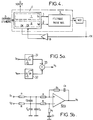
- the circuit 3 for calculating the average value in fact constitutes a low-pass filter type circuit ensuring the functions of integration and algebraic summation of the signals of first and second pulse S imp, S p delivered by the first, respectively the second channel 1.2.
- the subtractor circuit 33 can comprise, as shown in FIG. 5a, a first and a second integrator circuit 31, 32 receiving respectively the first and the second pulse S1, S p and delivering a corresponding integrated signal, and a subtractor circuit 33 receiving on its positive and negative inputs the integrated signal delivered by the first respectively the second integrator circuit 31,32.
- the subtractor circuit 33 delivers the phase comparison signal V0.
- this type of circuit can be produced, as shown in FIG. 5b, from an operational amplifier 300 mounted as a differential amplifier and looped back in feedback through a series circuit R1C1 on the negative input of the latter.
- phase comparator device object of the present invention, is particularly suitable for operation on the basis of data constituted by a digital signal of NRZ type for " no return to zero " in English language. Saxon.
- phase comparator device according to the invention due because it is adapted to detect transitions, can be used with all types of digital signal coding formats, such as RZ or CMI type codings for example.
Applications Claiming Priority (2)
| Application Number | Priority Date | Filing Date | Title |
|---|---|---|---|
| FR9407662A FR2721780B1 (fr) | 1994-06-22 | 1994-06-22 | Dispositif comparateur de phase. |
| FR9407662 | 1994-06-22 |
Publications (2)
| Publication Number | Publication Date |
|---|---|
| EP0689315A1 true EP0689315A1 (de) | 1995-12-27 |
| EP0689315B1 EP0689315B1 (de) | 2000-03-22 |
Family
ID=9464519
Family Applications (1)
| Application Number | Title | Priority Date | Filing Date |
|---|---|---|---|
| EP19950401435 Expired - Lifetime EP0689315B1 (de) | 1994-06-22 | 1995-06-19 | Phasenkomparator |
Country Status (3)
| Country | Link |
|---|---|
| EP (1) | EP0689315B1 (de) |
| DE (1) | DE69515735T2 (de) |
| FR (1) | FR2721780B1 (de) |
Cited By (5)
| Publication number | Priority date | Publication date | Assignee | Title |
|---|---|---|---|---|
| EP0874449A2 (de) * | 1997-04-24 | 1998-10-28 | Nortel Networks Corporation | Verfahren und Gerät zum Phasendetektieren in digitale Signalen |
| US6028898A (en) * | 1997-04-24 | 2000-02-22 | Nortel Networks Corporation | Signal regenerator |
| EP1677422A1 (de) * | 2004-12-30 | 2006-07-05 | Alcatel | Vorrichtung zur Umwandlung eines übertragenen Signals in ein digitales Signal |
| WO2008095508A1 (en) * | 2007-02-05 | 2008-08-14 | Tes Electronic Solutions Gmbh | Pulse generator |
| ITTO20130347A1 (it) * | 2013-04-29 | 2014-10-30 | St Microelectronics Srl | Circuito e metodo di calibrazione per un oscillatore controllato digitalmente |
Citations (3)
| Publication number | Priority date | Publication date | Assignee | Title |
|---|---|---|---|---|
| US4535459A (en) * | 1983-05-26 | 1985-08-13 | Rockwell International Corporation | Signal detection apparatus |
| EP0286329A2 (de) * | 1987-04-07 | 1988-10-12 | Gigabit Logic Inc | Synchronisator und Signaldetektor mit Phasenregelschleife |
| EP0500473A1 (de) * | 1991-02-22 | 1992-08-26 | SAT (Société Anonyme de Télécommunications) | Phasen/Frequenzkomparator für Taktrückgewinnungssystem |
-
1994
- 1994-06-22 FR FR9407662A patent/FR2721780B1/fr not_active Expired - Fee Related
-
1995
- 1995-06-19 DE DE1995615735 patent/DE69515735T2/de not_active Expired - Lifetime
- 1995-06-19 EP EP19950401435 patent/EP0689315B1/de not_active Expired - Lifetime
Patent Citations (3)
| Publication number | Priority date | Publication date | Assignee | Title |
|---|---|---|---|---|
| US4535459A (en) * | 1983-05-26 | 1985-08-13 | Rockwell International Corporation | Signal detection apparatus |
| EP0286329A2 (de) * | 1987-04-07 | 1988-10-12 | Gigabit Logic Inc | Synchronisator und Signaldetektor mit Phasenregelschleife |
| EP0500473A1 (de) * | 1991-02-22 | 1992-08-26 | SAT (Société Anonyme de Télécommunications) | Phasen/Frequenzkomparator für Taktrückgewinnungssystem |
Non-Patent Citations (2)
| Title |
|---|
| C.H.HOGGE: "A SELF CORRECTING CLOCK RECOVERY CIRCUIT", JOURNAL OF LIGHTWAVE TECHNOLOGY, vol. 3, no. 6, December 1985 (1985-12-01), pages 1312 - 1314 * |
| C.R. HOGGE: "A self correcting Clock Recovery Circuit", JOURNAL OF LIGHTWAVE TECHNOLOGY, vol. LT-3, no. 6, December 1985 (1985-12-01) |
Cited By (8)
| Publication number | Priority date | Publication date | Assignee | Title |
|---|---|---|---|---|
| EP0874449A2 (de) * | 1997-04-24 | 1998-10-28 | Nortel Networks Corporation | Verfahren und Gerät zum Phasendetektieren in digitale Signalen |
| EP0874449A3 (de) * | 1997-04-24 | 1999-11-10 | Nortel Networks Corporation | Verfahren und Gerät zur Phasendetektion in digitalen Signalen |
| US6028898A (en) * | 1997-04-24 | 2000-02-22 | Nortel Networks Corporation | Signal regenerator |
| EP1677422A1 (de) * | 2004-12-30 | 2006-07-05 | Alcatel | Vorrichtung zur Umwandlung eines übertragenen Signals in ein digitales Signal |
| FR2880482A1 (fr) * | 2004-12-30 | 2006-07-07 | Cit Alcatel | Dispositif de conversion d'un signal transmis en un signal numerique |
| WO2008095508A1 (en) * | 2007-02-05 | 2008-08-14 | Tes Electronic Solutions Gmbh | Pulse generator |
| ITTO20130347A1 (it) * | 2013-04-29 | 2014-10-30 | St Microelectronics Srl | Circuito e metodo di calibrazione per un oscillatore controllato digitalmente |
| US9231597B2 (en) | 2013-04-29 | 2016-01-05 | Stmicroelectronics S.R.L. | Digitally controlled oscillator calibration circuit and method |
Also Published As
| Publication number | Publication date |
|---|---|
| EP0689315B1 (de) | 2000-03-22 |
| FR2721780A1 (fr) | 1995-12-29 |
| DE69515735T2 (de) | 2000-11-09 |
| FR2721780B1 (fr) | 1996-08-30 |
| DE69515735D1 (de) | 2000-04-27 |
Similar Documents
| Publication | Publication Date | Title |
|---|---|---|
| EP2137874B1 (de) | Vorrichtung zur rückgewinnung des taktsignales zur digitalen regelung der phase ohne externe regelung | |
| EP0716501B1 (de) | Phasenvergleicher für ein digitales Signal und ein Taktsignal, und entsprechender Phasenregelkreis | |
| JPH05276028A (ja) | 非常に高い周波数のクロック及びデータ回復回路用の位相検知器 | |
| FR2880482A1 (fr) | Dispositif de conversion d'un signal transmis en un signal numerique | |
| EP0142440A2 (de) | Vorrichtung zum Erzeugen einer, bezüglich einer Referenzfrequenz gebrochenen Frequenz | |
| EP0015014A1 (de) | Vorrichtung zur schnellen Synchronisierung eines Taktsignals | |
| FR2509890A1 (fr) | Appareil de lecture de donnees pour la transmission de donnees | |
| US20020181360A1 (en) | Clock adjusting device for use with data reproducing apparatus, offset detecting device, and data reporducing apparatus | |
| EP0689315B1 (de) | Phasenkomparator | |
| FR2736231A1 (fr) | Systeme de communication numerique comportant un recepteur dote d'un dispositif de recuperation de rythme | |
| EP0680170A1 (de) | Übertragungsanordnung für ein Leitungskodiertes Signal über eine Fernsprechleitung mit Frequenzsynchronisierungsschaltung | |
| EP0026699A1 (de) | Verfahren und Vorrichtung zum Codieren binärer Daten, Vorrichtung zum Decodieren codierter Daten und solche Vorrichtungen enthaltendes Übertragungssystem | |
| EP0023852A1 (de) | Verfahren und Vorrichtung zur Phasenregelung eines lokalen Taktgebers | |
| EP0696116B1 (de) | Verfahren zum Abtasten eines seriellen digitalen Signals | |
| EP1073204B1 (de) | Anordnung zur Synchronisierung eines Bezugselements eines analogen Signals mit einem Taktsignal | |
| FR2646742A1 (fr) | Dispositif pour synchroniser un signal pseudo-binaire avec un signal d'horloge regeneree a sauts de phase | |
| CA2082288C (fr) | Methode et dispositif pour restituer un signal d'horloge rythmant la transmission de signaux recus | |
| EP0174880B1 (de) | Schaltungsanordnung zum Feststellen der Übergänge eines Datensignals in Bezug auf ein Taktsignal und diese Anordnung enthaltende Synchronisationseinrichtung | |
| FR2573592A1 (fr) | Circuit oscillateur asservi en phase a un signal de frequence predeterminee | |
| EP0905946B1 (de) | Reglung der Abtastung von Biphasensignalen | |
| FR2568738A1 (fr) | Dispositif de recuperation de signal d'horloge dans une transmission numerique | |
| FR2755552A1 (fr) | Dispositif de recopie d'un signal d'horloge d'entree a frequence non continue | |
| EP0237408B1 (de) | Verfahren und Anordnung zur asynchronen Takt-Wiedergewinnung für digitale Übertragungssysteme | |
| JP3618787B2 (ja) | 信号処理装置 | |
| EP0697768A1 (de) | Eine kalibrierte Impulsbreite erzeugender Detektor für den Übergang eines Logiksignals |
Legal Events
| Date | Code | Title | Description |
|---|---|---|---|
| PUAI | Public reference made under article 153(3) epc to a published international application that has entered the european phase |
Free format text: ORIGINAL CODE: 0009012 |
|
| 17P | Request for examination filed |
Effective date: 19951027 |
|
| AK | Designated contracting states |
Kind code of ref document: A1 Designated state(s): DE FR GB IT |
|
| RAP1 | Party data changed (applicant data changed or rights of an application transferred) |
Owner name: MHS |
|
| GRAG | Despatch of communication of intention to grant |
Free format text: ORIGINAL CODE: EPIDOS AGRA |
|
| GRAH | Despatch of communication of intention to grant a patent |
Free format text: ORIGINAL CODE: EPIDOS IGRA |
|
| 17Q | First examination report despatched |
Effective date: 19990721 |
|
| GRAH | Despatch of communication of intention to grant a patent |
Free format text: ORIGINAL CODE: EPIDOS IGRA |
|
| GRAA | (expected) grant |
Free format text: ORIGINAL CODE: 0009210 |
|
| AK | Designated contracting states |
Kind code of ref document: B1 Designated state(s): DE FR GB IT |
|
| REF | Corresponds to: |
Ref document number: 69515735 Country of ref document: DE Date of ref document: 20000427 |
|
| ITF | It: translation for a ep patent filed |
Owner name: SOCIETA' ITALIANA BREVETTI S.P.A. |
|
| GBT | Gb: translation of ep patent filed (gb section 77(6)(a)/1977) |
Effective date: 20000531 |
|
| PLBE | No opposition filed within time limit |
Free format text: ORIGINAL CODE: 0009261 |
|
| STAA | Information on the status of an ep patent application or granted ep patent |
Free format text: STATUS: NO OPPOSITION FILED WITHIN TIME LIMIT |
|
| 26N | No opposition filed | ||
| REG | Reference to a national code |
Ref country code: GB Ref legal event code: IF02 |
|
| PGFP | Annual fee paid to national office [announced via postgrant information from national office to epo] |
Ref country code: GB Payment date: 20090604 Year of fee payment: 15 |
|
| PGFP | Annual fee paid to national office [announced via postgrant information from national office to epo] |
Ref country code: IT Payment date: 20090627 Year of fee payment: 15 |
|
| GBPC | Gb: european patent ceased through non-payment of renewal fee |
Effective date: 20100619 |
|
| PG25 | Lapsed in a contracting state [announced via postgrant information from national office to epo] |
Ref country code: IT Free format text: LAPSE BECAUSE OF NON-PAYMENT OF DUE FEES Effective date: 20100619 |
|
| PG25 | Lapsed in a contracting state [announced via postgrant information from national office to epo] |
Ref country code: GB Free format text: LAPSE BECAUSE OF NON-PAYMENT OF DUE FEES Effective date: 20100619 |
|
| PGFP | Annual fee paid to national office [announced via postgrant information from national office to epo] |
Ref country code: FR Payment date: 20110629 Year of fee payment: 17 |
|
| REG | Reference to a national code |
Ref country code: DE Ref legal event code: R082 Ref document number: 69515735 Country of ref document: DE Representative=s name: RAU, SCHNECK & HUEBNER PATENT- UND RECHTSANWAE, DE |
|
| REG | Reference to a national code |
Ref country code: DE Ref legal event code: R082 Ref document number: 69515735 Country of ref document: DE Representative=s name: RAU, SCHNECK & HUEBNER PATENTANWAELTE RECHTSAN, DE Effective date: 20120110 Ref country code: DE Ref legal event code: R081 Ref document number: 69515735 Country of ref document: DE Owner name: ATMEL CORP., US Free format text: FORMER OWNER: MHS, NANTES CEDEX, FR Effective date: 20120110 |
|
| PGFP | Annual fee paid to national office [announced via postgrant information from national office to epo] |
Ref country code: DE Payment date: 20120627 Year of fee payment: 18 |
|
| REG | Reference to a national code |
Ref country code: FR Ref legal event code: ST Effective date: 20130228 |
|
| PG25 | Lapsed in a contracting state [announced via postgrant information from national office to epo] |
Ref country code: FR Free format text: LAPSE BECAUSE OF NON-PAYMENT OF DUE FEES Effective date: 20120702 |
|
| REG | Reference to a national code |
Ref country code: DE Ref legal event code: R119 Ref document number: 69515735 Country of ref document: DE Effective date: 20140101 |
|
| PG25 | Lapsed in a contracting state [announced via postgrant information from national office to epo] |
Ref country code: DE Free format text: LAPSE BECAUSE OF NON-PAYMENT OF DUE FEES Effective date: 20140101 |